Ordering number : EN6681C
3LP01S
P-Channel Small Signal MOSFET
http://onsemi.com
–30V, –0.1A, 10.4Ω, Single SMCP
Features
•
•
•
Low ON-resistance
Ultrahigh-speed switching
2.5V drive
Specifications
Absolute Maximum Ratings at Ta=25°C
Parameter
Symbol
Drain to Source Voltage
Conditions
Ratings
VDSS
VGSS
Gate to Source Voltage
Drain Current (DC)
Unit
--30
V
±10
V
Allowable Power Dissipation
ID
IDP
PD
0.15
W
Channel Temperature
Tch
150
°C
Storage Temperature
Tstg
--55 to +150
°C
Drain Current (Pulse)
PW≤10μs, duty cycle≤1%
--0.1
A
--0.4
A
This product is designed to “ESD immunity < 200V*”, so please take care when handling.
* Machine Model
Stresses exceeding Maximum Ratings may damage the device. Maximum Ratings are stress ratings only. Functional operation above the Recommended Operating
Conditions is not implied. Extended exposure to stresses above the Recommended Operating Conditions may affect device reliability.
Package Dimensions
Ordering & Package Information
unit : mm (typ)
7013A-013
Shipping
memo
3LP01S-TL-E
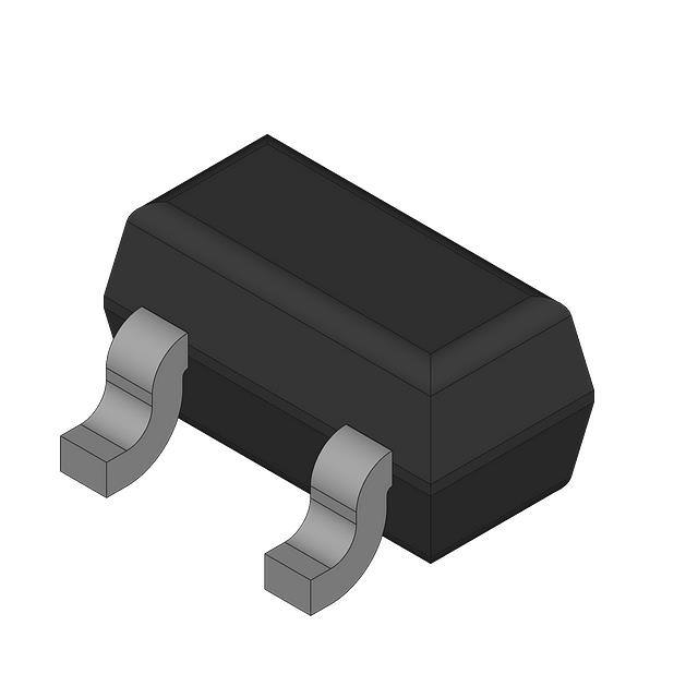
SMCP
SC-75,SOT-416
3,000
pcs./reel
Pb-Free
0.4
Marking
0.3
0.2
Packing Type: TL
1
2
3
0.1
0.75
0.6
0 to 0.1
0.1 MIN
1 : Gate
2 : Source
3 : Drain
SMCP
XA
LOT No.
LOT No.
1.6
0.5 0.5
Package
3LP01S-TL-E
1.6
0.8
0.4
Device
TL
Electrical Connection
3
1
2
Semiconductor Components Industries, LLC, 2013
June, 2013
62613 TKIM TC-00002948/62712 TKIM/41006PE MSIM TB-00002191/12201 TSIM TA-2005 No.6681-1/6
�3LP01S
Electrical Characteristics at Ta=25°C
Parameter
Symbol
Drain to Source Breakdown Voltage
Conditions
V(BR)DSS
IDSS
IGSS
VGS=±8V, VDS=0V
Forward Transfer Admittance
VGS(off)
| yfs |
VDS= --10V, ID= --100μA
VDS= --10V, ID= --50mA
Static Drain to Source On-State Resistance
RDS(on)1
RDS(on)2
ID= --50mA, VGS= --4V
ID= --30mA, VGS= --2.5V
ID= --1mA, VGS= --1.5V
Zero-Gate Voltage Drain Current
Gate to Source Leakage Current
Cutoff Voltage
RDS(on)3
Input Capacitance
Ciss
Output Capacitance
Coss
Reverse Transfer Capacitance
Crss
Turn-ON Delay Time
td(on)
tr
Rise Time
Turn-OFF Delay Time
Fall Time
td(off)
tf
Total Gate Charge
Qg
Gate to Source Charge
Qgs
Gate to Drain “Miller” Charge
Qgd
Diode Forward Voltage
VSD
ID= --1mA, VGS=0V
VDS= --30V, VGS=0V
VDS= --10V, f=1MHz
See specified Test Circuit.
VDS= --10V, VGS= --10V, ID= --100mA
Ratings
min
typ
max
--30
V
--0.4
80
--1
μA
±10
μA
--1.4
110
V
mS
8
10.4
Ω
11
15.4
Ω
27
54
Ω
7.5
pF
5.7
pF
1.8
pF
24
ns
55
ns
120
ns
130
ns
1.43
nC
0.18
nC
0.25
IS= --100mA, VGS=0V
Unit
--0.83
nC
--1.2
V
Switching Time Test Circuit
0V
--4V
VDD= --15V
VIN
VIN
PW=10μs
D.C.≤1%
D
ID= --50mA
RL=300Ω
VOUT
G
3LP01S
P.G
50Ω
S
No.6681-2/6
�3LP01S
ID -- VDS
--2
--0.18
--0.16
Drain Current, ID -- A
V
--2.0V
--6.0
--0.07
--0.06
--0.05
--0.04
--0.03
VGS= --1.5V
--0.02
--0.10
--0.08
--0.06
0
--0.2
0
--0.4 --0.6
--0.8
--1.0
--1.2
--1.4
--1.6
Drain to Source Voltage, VDS -- V
--1.8
--2.0
0
Static Drain to Source
On-State Resistance, RDS(on) -- Ω
20
15
--50mA
ID= --30mA
5
0
--1
--2
--3
--4
--5
--6
--7
--8
Gate to Source Voltage, VGS -- V
--9
Ta=75°C
25°C
--25°C
7
5
3
2
1.0
--0.01
2
3
5
7
2
--0.1
Drain Current, ID -- A
,
mA
2.5
= -S
VG
30
-I D=
10
A,
50m
-I D=
8
V
4.0
= -V GS
6
4
2
--60
--40
--20
0
20
40
60
80
3
2
2
3
5
100
Ambient Temperature, Ta -- °C
120
140
7
--0.1
160
IT00083
2
3
IT00080
RDS(on) -- ID
VGS= --1.5V
5
3
2
100
7
5
3
Ta=75°C
2
--25°C
2
3
25°C
5
7
--1.0
Drain Current, ID -- mA
Forward Transfer Admittance, | yfs | -- S
V
12
--25°C
5
2
3
IT00082
| yfs | -- ID
1.0
16
14
7
IT00081
RDS(on) -- Ta
18
25°C
Ta=75°C
10
10
--0.1
3
--4.0
IT00078
2
Drain Current, ID -- A
Static Drain to Source
On-State Resistance, RDS(on) -- Ω
3
--3.5
3
7
5
10
--3.0
VGS= --4V
IT00079
VGS= --2.5V
2
--2.5
RDS(on) -- ID
1000
7
--2.0
5
1.0
--0.01
--10
RDS(on) -- ID
100
--1.5
7
25
0
--1.0
100
Ta=25°C
10
--0.5
Gate to Source Voltage, VGS -- V
IT00077
RDS(on) -- VGS
30
Static Drain to Source
On-State Resistance, RDS(on) -- Ω
--0.12
25°C
--0.02
0
Static Drain to Source
On-State Resistance, RDS(on) -- Ω
--0.14
--0.04
--0.01
Static Drain to Source
On-State Resistance, RDS(on) -- Ω
VDS= --10V
Ta=
--25
°C
--3
.0V
--4
.
--0.08
Drain Current, ID -- A
.
0V
--3.5V
--0.09
ID -- VGS
--0.20
5V
75°
C
--0.10
VDS= --10V
7
5
3
25°C
2
5°C
2
Ta= --
0.1
75°C
7
5
3
2
0.01
--0.01
2
3
5
7
--0.1
Drain Current, ID -- A
2
3
IT00084
No.6681-3/6
�3LP01S
IS -- VSD
3
Switching Time, SW Time -- ns
5
--0.01
--0.5
--0.6
--0.7
--25°C
2
25°C
3
Ta=7
5°C
--0.8
--0.9
--1.0
Diode Forward Voltage, VSD -- V
td(off)
100
7
5
tr
3
td(on)
2
3
2
10
Ciss
Coss
5
3
2
Crss
3
5
7
Drain Current, ID -- A
--0.1
IT00086
VGS -- Qg
VDS= --10V
ID= --0.1A
--9
7
2
--10
5
Ciss, Coss, Crss -- pF
tf
2
f=1MHz
7
--8
--7
--6
--5
--4
--3
--2
--1
0
1.0
0
--5
--10
--15
--20
--25
Drain to Source Voltage, VDS -- V
--30
IT00087
0
0.2
0.4
0.6
0.8
1.0
1.2
Total Gate Charge, Qg -- nC
1.4
1.6
IT00088
PD -- Ta
0.20
Allowable Power Dissipation, PD -- W
3
IT00085
Ciss, Coss, Crss -- VDS
100
5
10
--0.01
--1.1
Gate to Source Voltage, VGS -- V
Source Current, IS -- A
7
VDD= --15V
VGS= --4V
7
2
--0.1
SW Time -- ID
1000
VGS=0V
0.15
0.10
0.05
0
0
20
40
60
80
100
120
Ambient Temperature, Ta -- °C
140
160
IT02381
No.6681-4/6
�3LP01S
Outline Drawing
3LP01S-TL-E
Land Pattern Example
Mass (g) Unit
0.003 mm
* For reference
Unit: mm
0.7
1.3
0.7
0.7
0.6
0.5
0.5
No.6681-5/6
�3LP01S
Note on usage : Since the 3LP01S is a MOSFET product, please avoid using this device in the vicinity of
highly charged objects.
ON Semiconductor and the ON logo are registered trademarks of Semiconductor Components Industries, LLC (SCILLC). SCILLC owns the rights to a number
of patents, trademarks, copyrights, trade secrets, and other intellectual property. A listing of SCILLC’s product/patent coverage may be accessed at
www.onsemi.com/site/pdf/Patent-Marking.pdf. SCILLC reserves the right to make changes without further notice to any products herein. SCILLC makes no
warranty, representation or guarantee regarding the suitability of its products for any particular purpose, nor does SCILLC assume any liability arising out of the
application or use of any product or circuit, and specifically disclaims any and all liability, including without limitation special, consequential or incidental
damages. “Typical” parameters which may be provided in SCILLC data sheets and/or specifications can and do vary in different applications and actual
performance may vary over time. All operating parameters, including “Typicals” must be validated for each customer application by customer’s technical
experts. SCILLC does not convey any license under its patent rights nor the rights of others. SCILLC products are not designed, intended, or authorized for use
as components in systems intended for surgical implant into the body, or other applications intended to support or sustain life, or for any other application in
which the failure of the SCILLC product could create a situation where personal injury or death may occur. Should Buyer purchase or use SCILLC products for
any such unintended or unauthorized application, Buyer shall indemnify and hold SCILLC and its officers, employees, subsidiaries, affiliates, and distributors
harmless against all claims, costs, damages, and expenses, and reasonable attorney fees arising out of, directly or indirectly, any claim of personal injury or
death associated with such unintended or unauthorized use, even if such claim alleges that SCILLC was negligent regarding the design or manufacture of the
part. SCILLC is an Equal Opportunity/Affirmative Action Employer. This literature is subject to all applicable copyright laws and is not for resale in any manner.
PS No.6681-6/6
�


 工商网监
湘ICP备2023018690号
工商网监
湘ICP备2023018690号
