SGM2037
500mA, Low Noise, Very Low Dropout
Bias Rail CMOS Voltage Regulator
GENERAL DESCRIPTION
FEATURES
The SGM2037 is a low noise, low dropout voltage
● 500mA Nominal Output Current
linear regulator which is designed using CMOS
● Input Voltage Range: 0.8V to 5.5V
technology. It provides 500mA output current capability.
● Bias Voltage Range: 2.5V to 5.5V
The operating input voltage range is from 0.8V to 5.5V
● Fixed Output Voltages: 0.8V, 0.9V, 1.0V, 1.05V,
and bias supply voltage range is from 2.5V to 5.5V. The
1.1V, 1.15V, 1.2V, 1.25V, 1.3V, 1.5V, 1.8V, 2.5V, 2.8V,
output voltage range is from 0.8V to 3.6V.
3.0V, 3.3V, and 3.6V
Other features include logic-controlled shutdown mode,
short-circuit
current
limit
and
thermal
shutdown
protection. The SGM2037 has automatic discharge
function to quickly discharge VOUT in the disabled status.
The SGM2037 is suitable for applications which need
low noise, fast transient response and low IQ
consumption, such as battery-powered equipment and
smartphones, etc.
● Adjustable Output Voltage Range: 0.8V to 3.6V
● Output Voltage Accuracy: ±0.8% at +25℃
● Low Dropout Voltage: 120mV (TYP) at 500mA
● Very Low Bias Input Current: 37μA (TYP)
● Very Low Bias Input Current in Shutdown:
0.01μA (TYP)
● Low Noise: 25μVRMS (TYP)
● Over-Current and Over-Temperature Protections
● Fast Load Transient Response
The SGM2037 is available in Green SOT-23-5, SOT-23-6
● Logic Level Enable Input for ON/OFF Control
and UTDFN-1.2×1.2-6L packages. It operates over an
● -40℃ to +125℃ Operating Temperature Range
ambient temperature range of -40℃ to +125℃.
● Available in Green SOT-23-5, SOT-23-6 and
UTDFN-1.2×1.2-6L Packages
APPLICATIONS
Portable Equipment
Smartphone
Industrial and Medical Equipment
TYPICAL APPLICATION
VIN
CIN
1μF
IN
ON
EN
OFF
VBIAS
BIAS
CBIAS
0.1μF
VOUT
OUT
SGM2037
GND
COUT
2.2μF
Figure 1. Fixed Voltage Typical Application Circuit
SG Micro Corp
www.sg-micro.com
VIN
CIN
1μF
IN
ON
EN
OFF
VBIAS
SGM2037-ADJ
BIAS
CBIAS
0.1μF
VOUT
OUT
GND
R1
FB
COUT
2.2μF
R2
Figure 2. Adjustable Voltage Typical Application Circuit
SEPTEMBER 2018 – REV. A
�500mA, Low Noise, Very Low Dropout
Bias Rail CMOS Voltage Regulator
SGM2037
PACKAGE/ORDERING INFORMATION
MODEL
PACKAGE
DESCRIPTION
SPECIFIED
TEMPERATURE
RANGE
ORDERING
NUMBER
PACKAGE
MARKING
PACKING
OPTION
SGM2037-0.8
SOT-23-5
-40℃ to +125℃
SGM2037-0.8XN5G/TR
GP6XX
Tape and Reel, 3000
SGM2037-0.9
SOT-23-5
-40℃ to +125℃
SGM2037-0.9XN5G/TR
GV1XX
Tape and Reel, 3000
SGM2037-1.0
SOT-23-5
-40℃ to +125℃
SGM2037-1.0XN5G/TR
GV2XX
Tape and Reel, 3000
SGM2037-1.05
SOT-23-5
-40℃ to +125℃
SGM2037-1.05XN5G/TR
GV3XX
Tape and Reel, 3000
SGM2037-1.1
SOT-23-5
-40℃ to +125℃
SGM2037-1.1XN5G/TR
GV4XX
Tape and Reel, 3000
SGM2037-1.15
SOT-23-5
-40℃ to +125℃
SGM2037-1.15XN5G/TR
GV5XX
Tape and Reel, 3000
SGM2037-1.2
SOT-23-5
-40℃ to +125℃
SGM2037-1.2XN5G/TR
GV6XX
Tape and Reel, 3000
SGM2037-1.25
SOT-23-5
-40℃ to +125℃
SGM2037-1.25XN5G/TR
GV7XX
Tape and Reel, 3000
SGM2037-1.3
SOT-23-5
-40℃ to +125℃
SGM2037-1.3XN5G/TR
GV8XX
Tape and Reel, 3000
SGM2037-1.5
SOT-23-5
-40℃ to +125℃
SGM2037-1.5XN5G/TR
GV9XX
Tape and Reel, 3000
SGM2037-1.8
SOT-23-5
-40℃ to +125℃
SGM2037-1.8XN5G/TR
GVAXX
Tape and Reel, 3000
SGM2037-2.5
SOT-23-5
-40℃ to +125℃
SGM2037-2.5XN5G/TR
GVBXX
Tape and Reel, 3000
SGM2037-2.8
SOT-23-5
-40℃ to +125℃
SGM2037-2.8XN5G/TR
GVCXX
Tape and Reel, 3000
SGM2037-3.0
SOT-23-5
-40℃ to +125℃
SGM2037-3.0XN5G/TR
GVDXX
Tape and Reel, 3000
SGM2037-3.3
SOT-23-5
-40℃ to +125℃
SGM2037-3.3XN5G/TR
GVEXX
Tape and Reel, 3000
SGM2037-3.6
SOT-23-5
-40℃ to +125℃
SGM2037-3.6XN5G/TR
M35XX
Tape and Reel, 3000
SGM2037-ADJ
SOT-23-6
-40℃ to +125℃
SGM2037-ADJXN6G/TR
GVFXX
Tape and Reel, 3000
SGM2037-0.8
UTDFN-1.2×1.2-6L
-40℃ to +125℃
SGM2037-0.8XUDX6G/TR
SGM2037-0.9
UTDFN-1.2×1.2-6L
-40℃ to +125℃
SGM2037-0.9XUDX6G/TR
SGM2037-1.0
UTDFN-1.2×1.2-6L
-40℃ to +125℃
SGM2037-1.0XUDX6G/TR
SGM2037-1.05
UTDFN-1.2×1.2-6L
-40℃ to +125℃
SGM2037-1.05XUDX6G/TR
SGM2037-1.1
UTDFN-1.2×1.2-6L
-40℃ to +125℃
SGM2037-1.1XUDX6G/TR
SGM2037-1.15
UTDFN-1.2×1.2-6L
-40℃ to +125℃
SGM2037-1.15XUDX6G/TR
SGM2037-1.2
UTDFN-1.2×1.2-6L
-40℃ to +125℃
SGM2037-1.2XUDX6G/TR
SGM2037-1.25
UTDFN-1.2×1.2-6L
-40℃ to +125℃
SGM2037-1.25XUDX6G/TR
SGM2037-1.3
UTDFN-1.2×1.2-6L
-40℃ to +125℃
SGM2037-1.3XUDX6G/TR
SGM2037-1.5
UTDFN-1.2×1.2-6L
-40℃ to +125℃
SGM2037-1.5XUDX6G/TR
SGM2037-1.8
UTDFN-1.2×1.2-6L
-40℃ to +125℃
SGM2037-1.8XUDX6G/TR
SGM2037-2.5
UTDFN-1.2×1.2-6L
-40℃ to +125℃
SGM2037-2.5XUDX6G/TR
SG Micro Corp
www.sg-micro.com
36
XX
Z9
XX
ZA
XX
ZB
XX
ZC
XX
ZD
XX
ZE
XX
ZF
XX
00
XX
01
XX
02
XX
03
XX
Tape and Reel, 5000
Tape and Reel, 5000
Tape and Reel, 5000
Tape and Reel, 5000
Tape and Reel, 5000
Tape and Reel, 5000
Tape and Reel, 5000
Tape and Reel, 5000
Tape and Reel, 5000
Tape and Reel, 5000
Tape and Reel, 5000
Tape and Reel, 5000
SEPTEMBER 2018
2
�500mA, Low Noise, Very Low Dropout
Bias Rail CMOS Voltage Regulator
SGM2037
PACKAGE/ORDERING INFORMATION (continued)
MODEL
PACKAGE
DESCRIPTION
SPECIFIED
TEMPERATURE
RANGE
ORDERING
NUMBER
SGM2037-2.8
UTDFN-1.2×1.2-6L
-40℃ to +125℃
SGM2037-2.8XUDX6G/TR
SGM2037-3.0
UTDFN-1.2×1.2-6L
-40℃ to +125℃
SGM2037-3.0XUDX6G/TR
SGM2037-3.3
UTDFN-1.2×1.2-6L
-40℃ to +125℃
SGM2037-3.3XUDX6G/TR
SGM2037-3.6
UTDFN-1.2×1.2-6L
-40℃ to +125℃
SGM2037-3.6XUDX6G/TR
SGM2037-ADJ
UTDFN-1.2×1.2-6L
-40℃ to +125℃
SGM2037-ADJXUDX6G/TR
PACKAGE
MARKING
04
XX
05
XX
06
XX
37
XX
07
XX
PACKING
OPTION
Tape and Reel, 5000
Tape and Reel, 5000
Tape and Reel, 5000
Tape and Reel, 5000
Tape and Reel, 5000
MARKING INFORMATION
NOTE: XX = Date Code.
SOT-23-6/SOT-23-5
YYY X X
Date Code - Month
Date Code - Year
Serial Number
UTDFN-1.2×1.2-6L
YY
XX
Serial Number
Date Code - Month
Date Code - Year
Green (RoHS & HSF): SG Micro Corp defines "Green" to mean Pb-Free (RoHS compatible) and free of halogen substances. If
you have additional comments or questions, please contact your SGMICRO representative directly.
ABSOLUTE MAXIMUM RATINGS
OVERSTRESS CAUTION
IN, BIAS, EN to GND ........................................... -0.3V to 6V
OUT, FB to GND .................................... -0.3V to (VIN + 0.3V)
Power Dissipation, PD @ TA = +25℃
SOT-23-5 ................................................................... 584mW
SOT-23-6 ................................................................... 641mW
UTDFN-1.2×1.2-6L .................................................... 612mW
Package Thermal Resistance
SOT-23-5, θJA .......................................................... 214℃/W
SOT-23-6, θJA .......................................................... 195℃/W
UTDFN-1.2×1.2-6L, θJA ........................................... 204℃/W
Junction Temperature .................................................+150℃
Storage Temperature Range ........................ -65℃ to +150℃
Lead Temperature (Soldering, 10s).............................+260℃
ESD Susceptibility
HBM ............................................................................. 8000V
MM ................................................................................. 400V
CDM ............................................................................ 1000V
This integrated circuit can be damaged if ESD protections are
not considered carefully. It recommends that all integrated
circuits be handled with appropriate precautions. Failure to
observe proper handling and installation procedures can
cause damage. ESD damage can range from subtle
performance degradation to complete device failure. Precision
integrated circuits may be more susceptible to damage
because even small parametric changes could cause the
device not to meet the published specifications.
RECOMMENDED OPERATING CONDITIONS
DISCLAIMER
Operating Input Voltage Range, VIN ....................0.8V to 5.5V
Operating Bias Voltage Range, VBIAS..................2.5V to 5.5V
BIAS Effective Capacitance, CBIAS ...................... 0.1μF (MIN)
Input Effective Capacitance, CIN ......................... 0.5μF (MIN)
Output Effective Capacitance, COUT .................... 1μF to 10μF
Operating Temperature Range ..................... -40℃ to +125℃
SG Micro Corp
www.sg-micro.com
Stresses beyond those listed in Absolute Maximum Ratings
may cause permanent damage to the device. Exposure to
absolute maximum rating conditions for extended periods
may affect reliability. Functional operation of the device at any
conditions beyond those indicated in the Recommended
Operating Conditions section is not implied.
ESD SENSITIVITY CAUTION
We reserve the right to make any change in circuit design, or
specifications without prior notice.
SEPTEMBER 2018
3
�500mA, Low Noise, Very Low Dropout
Bias Rail CMOS Voltage Regulator
SGM2037
PIN CONFIGURATIONS
SGM2037-Fixed Output
IN
1
GND
2
BIAS
3
SGM2037-ADJ
5
4
OUT
EN
IN
1
6
OUT
GND
2
5
FB
BIAS
3
4
EN
SOT-23-5
SOT-23-6
SGM2037-Fixed Output
SGM2037-ADJ
OUT
1
6
IN
GND
FB
2
5
GND
BIAS
EN
3
4
BIAS
OUT
1
6
IN
NC
2
5
EN
3
4
UTDFN-1.2×1.2-6L
UTDFN-1.2×1.2-6L
PIN DESCRIPTION
PIN
NAME
SOT-23-5
SOT-23-6
UTDFN1.2×1.2-6L
1
1
6
IN
2
2
5
GND
3
3
4
BIAS
4
4
3
EN
5
6
1
OUT
‒
5
2
‒
‒
‒
SG Micro Corp
www.sg-micro.com
FB
NC
Exposed
Pad
‒
FUNCTION
Input Voltage Supply Pin.
Ground.
Bias Voltage Supply for Internal Control Circuits. This pin is
monitored by internal under-voltage lockout circuit.
Enable Pin. Drive EN high to turn on the regulator. Drive EN low to
turn off the regulator. The EN pin has an internal pull-down
resistance which ensures that the device is turned off when the
EN pin is floated.
Regulated Output Voltage Pin. It is recommended to use output
capacitor with effective capacitance in the range of 1μF to 10μF.
Feedback Pin (adjustable voltage version only). Connect this pin to
the midpoint of an external resistor divider to adjust the output
voltage.
No Connection (fixed voltage version).
Exposed Pad. Exposed pad is internally connected to GND.
Connect it to a large ground plane to maximize thermal
performance; not intended as an electrical connection point.
SEPTEMBER 2018
4
�500mA, Low Noise, Very Low Dropout
Bias Rail CMOS Voltage Regulator
SGM2037
ELECTRICAL CHARACTERISTICS
(VBIAS = 2.7V or (VOUT(NOM) + 1.6V), whichever is greater, VEN = VBIAS, VIN = VOUT(NOM) + 0.3V, IOUT = 1mA, CIN = 1μF, CBIAS = 0.1μF,
COUT = 2.2μF, Full = -40℃ to +125℃, unless otherwise noted.)
PARAMETER
SYMBOL
Operating Input Voltage Range
VIN
Operating Bias Voltage Range
VBIAS
Under-Voltage Lockout Threshold
VUVLO
Feedback Voltage
VFB
Output Voltage Accuracy
VOUT
∆VOUT
∆VIN × VOUT
VIN Line Regulation
Load Regulation
ΔVOUT
(1)
VBIAS Dropout Voltage
(1) (2)
Output Current Limit
Short Current Limit
FB Pin Input Current
VDROP_IN
VDROP_BIAS
+25℃
1.6
+25℃
0.2
SGM2037-ADJ, VOUT = VFB,
IOUT = 1mA to 500mA
VIN = (VOUT(NOM) + 0.3V) to (VOUT(NOM) + 1.0V),
VBIAS = 2.7V or (VOUT(NOM) + 1.6V) to 5.5V,
IOUT = 1mA to 500mA
VIN = (VOUT(NOM) + 0.3V) to 5.5V
Thermal Shutdown Temperature
Thermal Shutdown Hysteresis
0.8064
+25℃
0.7936
+25℃
-0.8
0.8
Full
-1.5
1.5
+25℃
0.005
0.1
IOUT = 1mA to 500mA, 0.8V ≤ VOUT(NOM) ≤ 1.8V +25℃
0.5
2
IOUT = 1mA to 500mA, 1.8V < VOUT(NOM) ≤ 3.6V +25℃
1
5
IOUT = 150mA
+25℃
35
50
IOUT = 500mA
+25℃
120
170
IOUT = 500mA
+25℃
1.2
1.5
VOUT = 0V
+25℃
+25℃
IFB
VEN = 0V
Output Discharge Resistance
V
0.03
IDIS_BIAS
Output Voltage Noise
V
0.002
VEN = 0V
VBIAS Power Supply Rejection Ratio
5.5
+25℃
IDIS_IN
VIN Power Supply Rejection Ratio
V
0.03
IN Pin Disable Current
Turn-On Time
5.5
0.002
VBIAS = 5.5V
EN Pin Pull-Down Resistance
0.8
MAX UNITS
+25℃
IBIAS
EN Pin Threshold Voltage
TYP
VBIAS rising
BIAS Pin Operating Current
BIAS Pin Disable Current
MIN
Hysteresis
ILIM
ISHORT
TEMP
VOUT(NOM) +
+25℃
VDROP_IN
(VOUT(NOM) +
+25℃
1.4) ≥ 2.5
VBIAS = 2.7V or (VOUT(NOM) + 1.6V) to 5.5V,
∆VOUT
0.8V ≤ VOUT(NOM) ≤ 1.8V
∆VBIAS × VOUT VBIAS = (VOUT(NOM) + 1.6V) to 5.5V,
1.8V < VOUT(NOM) ≤ 3.6V
VBIAS Line Regulation
VIN Dropout Voltage
CONDITIONS
-30
30
37
53
Full
55
0.1
Full
Full
VIL
EN input voltage low
Full
0.5
1.6
0.01
Full
EN input voltage high
mV
mV
V
mA
Full
+25℃
%/V
mA
20
+25℃
%/V
670
-20
+25℃
%
340
+25℃
VIH
REN
505
V
0.5
2.5
1.2
nA
μA
μA
μA
V
0.25
V
+25℃
580
kΩ
+25℃
100
μs
+25℃
71
+25℃
76
+25℃
25
μVRMS
+25℃
120
Ω
TSHDN
160
℃
ΔTSHDN
20
℃
tON
PSRR
en
RDISCH
From assertion of
VEN to VOUT = 90%VOUT(NOM)
VIN to VOUT, f = 1kHz, VOUT(NOM) = 1.0V,
IOUT = 150mA, VIN ≥ 1.5V
VBIAS to VOUT, f = 1kHz, VOUT(NOM) = 1.0V,
IOUT = 150mA, VIN ≥ 1.5V
VIN = VOUT(NOM) + 0.5V,
VOUT(NOM) = 1.0V, f = 10Hz to 100kHz
VEN = 0V, VOUT = 0.5V
dB
NOTES:
1. Dropout voltage is characterized when VOUT falls 5% below VOUT(NOM).
2. For output voltages below 1.5V, VBIAS dropout voltage does not apply due to a minimum bias operating voltage of 2.5V.
SG Micro Corp
www.sg-micro.com
SEPTEMBER 2018
5
�500mA, Low Noise, Very Low Dropout
Bias Rail CMOS Voltage Regulator
SGM2037
TYPICAL PERFORMANCE CHARACTERISTICS
TA = +25℃, VIN = 1.3V, VEN = VBIAS = 2.7V, VOUT(NOM) = 1.0V, CIN = 1μF, CBIAS = 0.1μF, COUT = 2.2μF, unless otherwise noted.
Turn-On Speed with EN Pin
Turn-Off Speed with EN Pin
1V/div
1V/div
VOUT
500mV/div
500mV/div
VEN
VEN
VOUT
IOUT = 0mA
IOUT = 0mA
Time (50μs/div)
Time (200μs/div)
VIN Line Transient Response
VBIAS Line Transient Response
VBIAS
20mV/div
20mV/div
VOUT
1V/div
500mV/div
VIN
VOUT
VIN = 1.3V to 2.3V, IOUT = 500mA
VBIAS = 2.7V to 3.7V, IOUT = 500mA
Time (10μs/div)
Time (20μs/div)
Load Transient Response
Load Transient Response
Time (50μs/div)
SG Micro Corp
www.sg-micro.com
IOUT
VOUT
IOUT = 10mA to 500mA
100mV/div
IOUT = 1mA to 500mA
100mV/div
VOUT
200mA/div
200mA/div
IOUT
Time (50μs/div)
SEPTEMBER 2018
6
�500mA, Low Noise, Very Low Dropout
Bias Rail CMOS Voltage Regulator
SGM2037
TYPICAL PERFORMANCE CHARACTERISTICS (continued)
TA = +25℃, VIN = 1.3V, VEN = VBIAS = 2.7V, VOUT(NOM) = 1.0V, CIN = 1μF, CBIAS = 0.1μF, COUT = 2.2μF, unless otherwise noted.
VIN Power-Up/Power-Down Output Waveform
VIN Power Ramp-Up/Ramp-Down Output Waveform
500mV/div
VIN
VOUT
500mV/div
VOUT
IOUT = 150mA
500mV/div
500mV/div
VIN
IOUT = 150mA
Time (200μs/div)
Time (500μs/div)
VBIAS Power-Up/Power-Down Output Waveform
VBIAS Power Ramp-Up/Ramp-Down Output Waveform
1V/div
VBIAS
1V/div
VBIAS
IOUT = 150mA
IOUT = 150mA
Time (1ms/div)
Time (500μs/div)
Output Noise Density vs. Frequency
VIN = 1.5V, ILOAD = 1mA
1.8
1.6
1.4
1.2
1
0.8
0.6
0.4
0.2
0
0.01
2
Output Noise Density (μV/√Hz)
Output Noise Density (μV/√Hz)
2
0.1
1
Frequency (kHz)
SG Micro Corp
www.sg-micro.com
500mV/div
500mV/div
VOUT
VOUT
10
100
Output Noise Density vs. Frequency
VIN = 1.5V, ILOAD = 500mA
1.8
1.6
1.4
1.2
1
0.8
0.6
0.4
0.2
0
0.01
0.1
1
10
100
Frequency (kHz)
SEPTEMBER 2018
7
�500mA, Low Noise, Very Low Dropout
Bias Rail CMOS Voltage Regulator
SGM2037
TYPICAL PERFORMANCE CHARACTERISTICS (continued)
90
VIN Power Supply Rejection Ratio vs. Frequency
VIN = 1.5V, IOUT = 150mA
80
70
60
50
COUT = 10μF
40
30
20
COUT = 2.2μF
10
0
0.01
0.1
1
10
100
VBIAS Power Supply Rejection Ratio (dB)
VIN Power Supply Rejection Ratio (dB)
TA = +25℃, VIN = 1.3V, VEN = VBIAS = 2.7V, VOUT(NOM) = 1.0V, CIN = 1μF, CBIAS = 0.1μF, COUT = 2.2μF, unless otherwise noted.
1000
120
VBIAS Power Supply Rejection Ratio vs. Frequency
VIN = 1.5V, IOUT = 150mA
100
80
COUT = 10μF
60
40
COUT = 2.2μF
20
0
0.01
0.1
1
Frequency (kHz)
VIN Dropout Voltage vs. Output Current
180
VBIAS Dropout Voltage (mV)
VIN Dropout Voltage (mV)
+125℃
120
+85℃
100
+25℃
80
-40℃
60
40
20
0
0
100
200
300
400
1000
+25℃
-40℃
600
400
200
0
100
BIAS Pin Operating Current (μA)
BIAS Pin Operating Current (μA)
37
36
35
34
33
32
31
200
300
Output Current (mA)
SG Micro Corp
www.sg-micro.com
300
400
500
400
BIAS Pin Operating Current vs. BIAS Voltage
40
38
100
200
Output Current (mA)
BIAS Pin Operating Current vs. Output Current
0
+125℃
+85℃
800
0
500
39
30
1000
1200
Output Current (mA)
40
100
VBIAS Dropout Voltage vs. Output Current
1400
160
140
10
Frequency (kHz)
500
38
36
34
32
30
28
26
24
22
20
IOUT = 500mA
2.0
2.5
3.0
3.5
4.0
4.5
5.0
5.5
BIAS Voltage (V)
SEPTEMBER 2018
8
�500mA, Low Noise, Very Low Dropout
Bias Rail CMOS Voltage Regulator
SGM2037
TYPICAL PERFORMANCE CHARACTERISTICS (continued)
TA = +25℃, VIN = 1.3V, VEN = VBIAS = 2.7V, VOUT(NOM) = 1.0V, CIN = 1μF, CBIAS = 0.1μF, COUT = 2.2μF, unless otherwise noted.
VIN Dropout Voltage vs. (VBIAS - VOUT)
400
IOUT = 100mA
-40℃
300
250
+25℃
200
+85℃
150
+125℃
100
50
0
IOUT = 300mA
350
VIN Dropout Voltage (mV)
VIN Dropout Voltage (mV)
350
VIN Dropout Voltage vs. (VBIAS - VOUT)
400
300
250
200
150
-40℃
100
0.5
1.0
1.5
2.0
2.5
3.0
3.5
4.0
4.5
0
5.0
0.5
1.0
1.5
2.0
300
250
200
-40℃ +25℃
150
+85℃ +125℃
100
50
3.0
3.5
4.0
4.5
5.0
VIN Dropout Voltage vs. Temperature
140
IOUT = 500mA
120
100
80
IOUT = 150mA
60
40
0.5
1.0
1.5
2.0
2.5
3.0
3.5
4.0
4.5
20
5.0
-40 -25 -10
5
VBIAS - VOUT (V)
Output Voltage vs. Temperature
3.6060
1.0010
3.6040
1.0005
3.6020
1.0000
0.9995
0.9990
VOUT(NOM) = 1.0V, VIN = 1.3V,
VEN = VBIAS = 2.7V, IOUT = 1mA,
UTDFN-1.2×1.2-6L
0.9985
-40 -25 -10
5
20 35 50 65 80 95 110 125
Temperature (℃)
SG Micro Corp
www.sg-micro.com
20 35 50 65 80 95 110 125
Temperature (℃)
Output Voltage (V)
Output Voltage (V)
2.5
160
VIN Dropout Voltage (mV)
VIN Dropout Voltage (mV)
180
IOUT = 500mA
350
0.9980
+125℃
VBIAS - VOUT (V)
VIN Dropout Voltage vs. (VBIAS - VOUT)
400
1.0015
+85℃
50
VBIAS - VOUT (V)
0
+25℃
Output Voltage vs. Temperature
3.6000
3.5980
3.5960
VOUT(NOM) = 3.6V, VIN = 3.9V,
VEN = VBIAS = 5.2V, IOUT = 1mA,
UTDFN-1.2×1.2-6L
3.5940
3.5920
-40 -25 -10
5
20 35 50 65 80 95 110 125
Temperature (℃)
SEPTEMBER 2018
9
�500mA, Low Noise, Very Low Dropout
Bias Rail CMOS Voltage Regulator
SGM2037
FUNCTIONAL BLOCK DIAGRAM
Current
Limit
IN
OUT
BIAS
Voltage
Reference
+
120Ω
R1
UVLO
Thermal
Shutdown
Control
Logic
R2
EN
REN
GND
SGM2037
Figure 3. Fixed Version Block Diagram
Current
Limit
IN
OUT
BIAS
Voltage
Reference
0.8V
+
120Ω
UVLO
FB
Thermal
Shutdown
Control
Logic
EN
REN
GND
SGM2037-ADJ
Figure 4. Adjustable Version Block Diagram
SG Micro Corp
www.sg-micro.com
SEPTEMBER 2018
10
�SGM2037
500mA, Low Noise, Very Low Dropout
Bias Rail CMOS Voltage Regulator
APPLICATION INFORMATION
The SGM2037 is a low noise high performance LDO
with fast transient response. It consumes only 37μA
(TYP) quiescent current and provides 500mA output
current. The SGM2037 provides protection functions
for output overload, output short-circuit condition and
overheating.
When the EN pin voltage is higher than 1.2V, the device
is in active state. The input voltage is regulated to the
output voltage and the automatic discharge transistor is
turned off.
The SGM2037 is suitable for applications which need
noise sensitive circuit such as battery-powered
equipment and smartphones.
The output voltage of the SGM2037-ADJ can be
adjusted from 0.8V to 3.6V. The FB pin will be
connected to two external resistors as shown in Figure 5.
The output voltage is determined by the following
equation:
Input Capacitor Selection (CIN)
The input decoupling capacitor is necessary to be
connected as close as possible to the IN pin for
ensuring the device stability. A 1μF or larger X7R or
X5R ceramic capacitor is selected to get good dynamic
performance.
When VIN is required to provide large current
instantaneously, a large effective input capacitor is
required. Multiple input capacitors can limit the input
tracking inductance. Adding more input capacitors is
available to restrict the ringing and to keep it below the
device absolute maximum ratings.
Adjustable Regulator
R
= VFB × 1+ 1
VOUT
R2
(1)
where:
VOUT is output voltage and VFB is the internal voltage
reference, VFB = 0.8V. Choose R2 = 40kΩ to maintain a
20μA minimum load.
VIN
CIN
1μF
IN
ON
EN
OFF
VBIAS
SGM2037-ADJ
BIAS
CBIAS
0.1μF
VOUT
OUT
GND
R1
FB
COUT
2.2μF
R2
Output Capacitor Selection (COUT)
The output decoupling capacitor should be located as
close as possible to the OUT pin. A 1μF or larger X7R
or X5R ceramic capacitor is selected to get good
dynamic performance. The minimum effective
capacitance of COUT that SGM2037 can remain stable
is 1μF. For ceramic capacitor, temperature, DC bias
and package size will change the effective capacitance,
so enough margin of COUT must be considered in
design. Larger capacitance and lower ESR COUT will
help improve the load transient response and increase
the high frequency PSRR.
Enable Operation
The SGM2037 uses the EN pin to enable/disable the
device and to deactivate/activate the output automatic
discharge function.
When the EN pin voltage is lower than 0.25V, the
device is in shutdown state. There is no current flowing
from IN pin to OUT pin. In this state, the automatic
discharge transistor is active to discharge the output
voltage through a 120Ω (TYP) resistor.
SG Micro Corp
www.sg-micro.com
Figure 5. Adjustable Output Voltage Application
Dropout Voltage
The SGM2037 specifies two dropout voltages because
there are two power supplies VIN and VBIAS and one
VOUT regulator output. VIN dropout voltage is defined as
the difference between VIN and VOUT when VOUT falls 5%
below VOUT(NOM). When the output voltage is lower than
1.5V, VBIAS dropout voltage is not applicable because
the minimum bias operating voltage is 2.5V.
When VOUT begins to decrease and VBIAS is high
enough, the VIN dropout voltage equals to VIN - VOUT.
VBIAS dropout voltage refers to VBIAS - VOUT when the IN
and BIAS pins are connected together and VOUT begins
to decrease.
Output Current Limit and Short-Circuit
Protection
When an overload event happens, the output current is
internally limited to 670mA (TYP). When the OUT pin is
shorted to ground, the short-circuit protection will limit
the output current to 340mA (TYP).
SEPTEMBER 2018
11
�SGM2037
500mA, Low Noise, Very Low Dropout
Bias Rail CMOS Voltage Regulator
APPLICATION INFORMATION (continued)
Thermal Shutdown
The SGM2037 can detect the temperature of die. When
the die temperature exceeds the threshold value of
thermal shutdown, the SGM2037 will be in shutdown
state and it will remain in this state until the die
temperature decreases to +140℃.
Power Dissipation (PD)
Thermal protection limits power dissipation in the
SGM2037. When power dissipation on pass element
(PD = (VIN - VOUT) × IOUT) is too much and the operating
junction temperature exceeds +160℃, the OTP circuit
starts the thermal shutdown function and turns the pass
element off.
Therefore, thermal analysis for the chosen application
is important to guarantee reliable performance over all
conditions. To guarantee reliable operation, the junction
temperature of the SGM2037 must not exceed 125℃.
The maximum allowable power dissipation depends on
the thermal resistance of the IC package, the PCB
layout, the rate of surrounding airflow, and the difference
between the junction temperature and ambient
temperature. The maximum power dissipation can be
approximated using the following equation:
SG Micro Corp
www.sg-micro.com
PD(MAX) = (TJ(MAX) - TA) / θJA
(2)
where TJ(MAX) is the maximum junction temperature, TA
is the ambient temperature, and θJA is the junction
-to-ambient thermal resistance.
Negatively Biased Output
When the output voltage is negative, the chip may not
start up due to parasitic effects. Ensure that the output
is greater than -0.3V under all conditions. If negatively
biased output is excessive and expected in the
application, a Schottky diode can be added between
the OUT pin and GND pin.
Reverse Current Protection
The NMOS power transistor has an inherent body
diode, this body diode will be forward biased when
VOUT > VIN. When VOUT > VIN, the reverse current
flowing from the OUT pin to the IN pin will damage the
SGM2037. If VOUT > (VIN + 0.3V) is expected in the
application, one external Schottky diode will be added
between the OUT pin and IN pin to protect the
SGM2037.
SEPTEMBER 2018
12
�500mA, Low Noise, Very Low Dropout
Bias Rail CMOS Voltage Regulator
SGM2037
TYPICAL APPLICATION CIRCUIT
+
-
VBAT
BIAS
IN
I/O
Processor
IC
SW
Switch-Mode
DC/DC
EN
I/O
FB
IN
OUT
SGM2037
To Other
Circuits
EN
GND
Load
GND
Figure 6. Used as DC/DC Post Regulator
REVISION HISTORY
NOTE: Page numbers for previous revisions may differ from page numbers in the current version.
Changes from Original (SEPTEMBER 2018) to REV.A
Page
Changed from product preview to production data .................................................................................................................................................All
SG Micro Corp
www.sg-micro.com
SEPTEMBER 2018
13
�PACKAGE INFORMATION
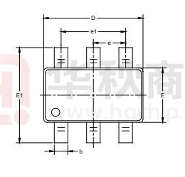
PACKAGE OUTLINE DIMENSIONS
SOT-23-5
1.90
D
e1
E1
2.59
E
0.99
b
e
0.69
0.95
RECOMMENDED LAND PATTERN (Unit: mm)
L
A
A1
θ
A2
Symbol
Dimensions
In Millimeters
MIN
MAX
c
0.2
Dimensions
In Inches
MIN
MAX
A
1.050
1.250
0.041
0.049
A1
0.000
0.100
0.000
0.004
A2
1.050
1.150
0.041
0.045
b
0.300
0.500
0.012
0.020
c
0.100
0.200
0.004
0.008
D
2.820
3.020
0.111
0.119
E
1.500
1.700
0.059
0.067
E1
2.650
2.950
0.104
0.116
e
0.950 BSC
0.037 BSC
e1
1.900 BSC
0.075 BSC
SG Micro Corp
www.sg-micro.com
L
0.300
0.600
0.012
0.024
θ
0°
8°
0°
8°
TX00033.000
�PACKAGE INFORMATION
PACKAGE OUTLINE DIMENSIONS
SOT-23-6
D
e1
e
2.59
E
E1
0.99
b
0.95
0.69
RECOMMENDED LAND PATTERN (Unit: mm)
L
A
A1
θ
A2
Symbol
Dimensions
In Millimeters
MIN
MAX
c
0.2
Dimensions
In Inches
MIN
MAX
A
1.050
1.250
0.041
0.049
A1
0.000
0.100
0.000
0.004
A2
1.050
1.150
0.041
0.045
b
0.300
0.500
0.012
0.020
c
0.100
0.200
0.004
0.008
D
2.820
3.020
0.111
0.119
E
1.500
1.700
0.059
0.067
E1
2.650
2.950
0.104
0.116
e
0.950 BSC
0.037 BSC
e1
1.900 BSC
0.075 BSC
SG Micro Corp
www.sg-micro.com
L
0.300
0.600
0.012
0.024
θ
0°
8°
0°
8°
TX00034.000
�PACKAGE INFORMATION
PACKAGE OUTLINE DIMENSIONS
UTDFN-1.2×1.2-6L
e
D
N6
N4
E
E1
D1
N1
N3
L
b
BOTTOM VIEW
TOP VIEW
0.89
0.30 1.80
A
A1
A2
0.55
SIDE VIEW
0.18
0.40
RECOMMENDED LAND PATTERN (Unit: mm)
Symbol
A
Dimensions In Millimeters
MIN
MOD
0.500
0.550
A1
0.600
0.050
A2
0.152 REF
e
SG Micro Corp
www.sg-micro.com
MAX
0.400 BSC
D
1.150
1.200
1.250
E
1.150
1.200
1.250
D1
0.840
0.890
0.940
E1
0.250
0.300
0.350
b
0.130
0.180
0.230
L
0.200
0.250
0.300
TX00143.000
�PACKAGE INFORMATION
TAPE AND REEL INFORMATION
REEL DIMENSIONS
TAPE DIMENSIONS
P2
W
P0
Q1
Q2
Q1
Q2
Q1
Q2
Q3
Q4
Q3
Q4
Q3
Q4
B0
Reel Diameter
A0
P1
K0
Reel Width (W1)
DIRECTION OF FEED
NOTE: The picture is only for reference. Please make the object as the standard.
KEY PARAMETER LIST OF TAPE AND REEL
Reel
Diameter
Reel Width
W1
(mm)
A0
(mm)
B0
(mm)
K0
(mm)
P0
(mm)
P1
(mm)
P2
(mm)
W
(mm)
Pin1
Quadrant
SOT-23-5
7″
9.5
3.20
3.20
1.40
4.0
4.0
2.0
8.0
Q3
SOT-23-6
7″
9.5
3.17
3.23
1.37
4.0
4.0
2.0
8.0
Q3
UTDFN-1.2×1.2-6L
7″
9.0
1.35
1.35
0.73
4.0
4.0
2.0
8.0
Q1
SG Micro Corp
www.sg-micro.com
TX10000.000
DD0001
Package Type
�PACKAGE INFORMATION
CARTON BOX DIMENSIONS
NOTE: The picture is only for reference. Please make the object as the standard.
KEY PARAMETER LIST OF CARTON BOX
Length
(mm)
Width
(mm)
Height
(mm)
Pizza/Carton
7″ (Option)
368
227
224
8
7″
442
410
224
18
SG Micro Corp
www.sg-micro.com
DD0002
Reel Type
TX20000.000
�


 工商网监
湘ICP备2023018690号
工商网监
湘ICP备2023018690号
