74LVC573A
OCTAL D-TYPE LATCH HIGH PERFORMANCE
s s s
s
s s
s
s
s
s
5V TOLERANT INPUTS HIGH SPEED: tPD = 6.8ns (MAX.) at VCC = 3V POWER DOWN PROTECTION ON INPUTS AND OUTPUTS SYMMETRICAL OUTPUT IMPEDANCE: |IOH| = IOL = 24mA (MIN) at VCC = 3V PCI BUS LEVELS GUARANTEED AT 24 mA BALANCED PROPAGATION DELAYS: tPLH ≅ tPHL OPERATING VOLTAGE RANGE: VCC(OPR) = 1.65V to 3.6V (1.2V Data Retention) PIN AND FUNCTION COMPATIBLE WITH 74 SERIES 573 LATCH-UP PERFORMANCE EXCEEDS 500mA (JESD 17) ESD PERFORMANCE: HBM > 2000V (MIL STD 883 method 3015); MM > 200V
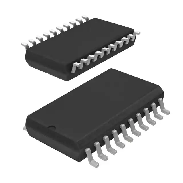
SOP
TSSOP
Table 1: Order Codes
PACKAGE SOP TSSOP T&R 74LVC573AMTR 74LVC573ATTR
DESCRIPTION The 74LVC573A is a low voltage CMOS OCTAL D-TYPE LATCH fabricated with sub-micron silicon gate and double-layer metal wiring C2MOS technology. It is ideal for 1.65 to 3.6 VCC operations and low power and low noise applications. These 8 bit D-Type latch are controlled by a latch enable input (LE) and an output enable input (OE). While the LE inputs is held at a high level, the Q Figure 1: Pin Connection And IEC Logic Symbols
outputs will follow the data input precisely or inversely. When the LE is taken low, the Q outputs will be latched precisely or inversely at the logic level of D input data. While the (OE) input is low, the 8 outputs will be in a normal logic state (high or low logic level) and while high level the outputs will be in a high impedance state. This device is designed to interface directly High Speed CMOS systems with TTL and NMOS components. It has more speed performance at 3.3V than 5V AC/ACT family, combined with a lower power consumption. All inputs are equipped with protection circuits against static discharge, giving them 2KV ESD immunity and transient excess voltage.
July 2004
Rev. 3
1/13
�74LVC573A
Figure 2: Input And Output Equivalent Circuit
Table 2: Pin Description
PIN N° 1 2, 3, 4, 5, 6, 7, 8, 9 12, 13, 14, 15, 16, 17, 18, 19 11 10 20 SYMBOL OE D0 to D7 Q0 to Q7 NAME AND FUNCTION 3 State Output Enable Input (Active LOW) Data Inputs 3-State Latch Outputs
Table 3: Truth Table
INPUTS OE H L L L
X : Don’t Care Z : High Impedance
OUTPUT D X X L H Q Z NO CHANGE L H
LE X L H H
LE GND VCC
Latch Enable Input Ground (0V) Positive Supply Voltage
Table 4: Absolute Maximum Ratings
Symbol VCC VI VO VO IIK IOK IO Supply Voltage DC Input Voltage DC Output Voltage (VCC = 0V) DC Output Voltage (High or Low State) (note 1) DC Input Diode Current DC Output Diode Current (note 2) DC Output Current Parameter Value -0.5 to +7.0 -0.5 to +7.0 -0.5 to +7.0 -0.5 to VCC + 0.5 - 50 - 50 ± 50 ± 100 -65 to +150 300 Unit V V V V mA mA mA mA °C °C
ICC or IGND DC VCC or Ground Current per Supply Pin Storage Temperature Tstg TL Lead Temperature (10 sec)
Absolute Maximum Ratings are those values beyond which damage to the device may occur. Functional operation under these conditions is not implied 1) IO absolute maximum rating must be observed 2) VO < GND
2/13
�74LVC573A
Table 5: Recommended Operating Conditions
Symbol VCC VI VO VO IOH, IOL IOH, IOL IOH, IOL IOH, IOL Top dt/dv Supply Voltage (note 1) Input Voltage Output Voltage (VCC = 0V) Output Voltage (High or Low State) High or Low Level Output Current (VCC = 3.0 to 3.6V) High or Low Level Output Current (VCC = 2.7 to 3.0V) High or Low Level Output Current (VCC = 2.3 to 2.7V) High or Low Level Output Current (VCC = 1.65 to 2.3V) Operating Temperature Input Rise and Fall Time (note 2) Parameter Value 1.65 to 3.6 0 to 5.5 0 to 5.5 0 to VCC ± 24 ± 12 ±8 ±4 -55 to 125 0 to 10 Unit V V V V mA mA mA mA °C ns/V
1) Truth Table guaranteed: 1.2V to 3.6V 2) VIN from 0.8V to 2V at VCC = 3.0V
Table 6: DC Specifications
Test Condition Symbol Parameter VCC (V) 1.65 to 1.95 2.3 to 2.7 2.7 to 3.6 1.65 to 1.95 2.3 to 2.7 2.7 to 3.6 1.65 to 3.6 1.65 2.3 2.7 3.0 3.0 VOL Low Level Output Voltage 1.65 to 3.6 1.65 2.3 2.7 3.0 II Ioff IOZ Input Leakage Current Power Off Leakage Current High Impedance Output Leakage Current Quiescent Supply Current ICC incr. per Input 3.6 0 3.6 IO=-100 µA IO=-4 mA IO=-8 mA IO=-12 mA IO=-18 mA IO=-24 mA IO=100 µA IO=4 mA IO=8 mA IO=12 mA IO=24 mA VI = 0 to 5.5V VI or VO = 5.5V VI = VIH or VIL VO = 0 to 5.5V VI = VCC or GND 3.6 2.7 to 3.6 VI or VO = 3.6 to 5.5V VIH = VCC-0.6V VCC-0.2 1.2 1.7 2.2 2.4 2.2 0.2 0.45 0.7 0.4 0.55 ±5 10 ±5 -40 to 85 °C Min. 0.65VCC 1.7 2 0.35VCC 0.7 0.8 VCC-0.2 1.2 1.7 2.2 2.4 2.2 0.2 0.45 0.7 0.4 0.55 ±5 10 ±5 µA µA µA V V Max. Value -55 to 125 °C Min. 0.65VCC 1.7 2 0.35VCC 0.7 0.8 V V Max. Unit
VIH
High Level Input Voltage Low Level Input Voltage High Level Output Voltage
VIL
VOH
ICC
10 ± 10 500
10 ± 10 500 µA µA 3/13
∆ICC
�74LVC573A
Table 7: Dynamic Switching Characteristics
Test Condition Symbol Parameter VCC (V) 3.3 CL = 50pF VIL = 0V, VIH = 3.3V Value TA = 25 °C Min. Typ. 0.8 -0.8 Max. V Unit
VOLP VOLV
Dynamic Low Level Quiet Output (note 1)
1) Number of output defined as "n". Measured with "n-1" outputs switching from HIGH to LOW or LOW to HIGH. The remaining output is measured in the LOW state.
Table 8: AC Electrical Characteristics
Test Condition Symbol Parameter VCC (V) 1.65 to 1.95 2.3 to 2.7 2.7 3.0 to 3.6 1.65 to 1.95 2.3 to 2.7 2.7 3.0 to 3.6 1.65 to 1.95 2.3 to 2.7 2.7 3.0 to 3.6 1.65 to 1.95 2.3 to 2.7 2.7 3.0 to 3.6 1.65 to 1.95 2.3 to 2.7 2.7 3.0 to 3.6 1.65 to 1.95 2.3 to 2.7 2.7 3.0 to 3.6 1.65 to 1.95 2.3 to 2.7 2.7 3.0 to 3.6 2.7 to 3.6 CL (pF) 30 30 50 50 30 30 50 50 30 30 50 50 30 30 50 50 30 30 50 50 30 30 50 50 30 30 50 50 RL (Ω ) 1000 500 500 500 1000 500 500 500 1000 500 500 500 1000 500 500 500 1000 500 500 500 1000 500 500 500 1000 500 500 500 ts = t r (ns) 2.0 2.0 2.5 2.5 2.0 2.0 2.5 2.5 2.0 2.0 2.5 2.5 2.0 2.0 2.5 2.5 2.0 2.0 2.5 2.5 2.0 2.0 2.5 2.5 2.0 2.0 2.5 2.5 -40 to 85 °C Min. Max. TBD TBD 7.8 6.8 TBD TBD 7.8 6.8 TBD TBD 8.7 7.7 TBD TBD 7.6 7.0 Value -55 to 125 °C Min. Max. TBD TBD 9.4 8.2 TBD TBD 9.4 8.2 TBD TBD 10.4 9.2 TBD TBD 9.1 8.4 Unit
tPLH tPHL
Propagation Delay Time D to Q
1.5 1
1.5 1
ns
tPLH tPHL
Propagation Delay Time LE to Q
1.5 1
1.5 1
ns
tPZL tPZH
Output Enable Time
1 1
1 1
ns
tPLZ tPHZ
Output Disable Time
tW
LE Pulse Width HIGH
ts
Setup Time D to LE, (HIGH to LOW)
th
Hold Time LE (HIGH to LOW) to D
2 2 TBD TBD 3.3 3.3 TBD TBD 2 2 TBD TBD 1.5 1.5
2 2 TBD TBD 3.3 3.3 TDB TBD 2 2 TBD TBD 1.5 1.5
ns
ns
ns
ns
tOSLH tOSHL
Output To Output Skew Time (note1, 2)
1
1
ns
1) Skew is defined as the absolute value of the difference between the actual propagation delay for any two outputs of the same device switching in the same direction, either HIGH or LOW (tOSLH = | tPLHm - tPLHn|, tOSHL = | tPHLm - tPHLn| 2) Parameter guaranteed by design
4/13
�74LVC573A
Table 9: Capacitive Characteristics
Test Condition Symbol Parameter VCC (V) Value TA = 25 °C Min. fIN = 10MHz Typ. 4 1.8 2.5 3.3 28 30 34 Max. pF pF Unit
CIN CPD
Input Capacitance Power Dissipation Capacitance (note 1)
1) CPD is defined as the value of the IC’s internal equivalent capacitance which is calculated from the operating current consumption without load. (Refer to Test Circuit). Average operating current can be obtained by the following equation. ICC(opr) = CPD x VCC x fIN + ICC/n (per circuit)
Figure 3: Test Circuit
RT = ZOUT of pulse generator (typically 50Ω)
Table 10: Test Circuit And Waveform Symbol Value
Symbol 1.65 to 1.95V CL RL = R1 VS VIH VM VOH VX VY tr = tr 30pF 1000Ω 2 x VCC VCC VCC/2 VCC VOL + 0.15V VOH - 0.15V


 工商网监
湘ICP备2023018690号
工商网监
湘ICP备2023018690号