VNH2SP30-E
AUTOMOTIVE FULLY INTEGRATED H-BRIDGE MOTOR DRIVER
Table 1. General Features
Type VNH2SP30-E RDS(on) 19 mΩ max (per leg)
Figure 1. Package
Iout
30 A Vccmax 41 V
s s
OUTPUT CURRENT: 30A
5V LOGIC LEVEL COMPATIBLE INPUTS s UNDERVOLTAGE AND OVERVOLTAGE SHUT-DOWN s OVERVOLTAGE CLAMP s THERMAL SHUT DOWN s CROSS-CONDUCTION PROTECTION s LINEAR CURRENT LIMITER s VERY LOW STAND-BY POWER CONSUMPTION s PWM OPERATION UP TO 20 KHz s PROTECTION AGAINST: LOSS OF GROUND AND LOSS OF VCC s CURRENT SENSE OUTPUT PROPORTIONAL TO MOTOR CURRENT s IN COMPLIANCE WITH THE 2002/95/EC EUROPEAN DIRECTIVE DESCRIPTION The VNH2SP30-E is a full bridge motor driver intended for a wide range of automotive applications. The device incorporates a dual monolithic High-Side drivers and two Low-Side switches. The High-Side driver switch is designed using STMicroelectronic’s well known and proven proprietary VIPower™ M0 technology that allows to efficiently integrate on the same die a true Power MOSFET with an intelligent signal/ protection circuitry. Table 2. Order Codes
Package Tube
VNH2SP30-E
MultiPowerSO-30
The Low-Side switches are vertical MOSFETs manufactured using STMicroelectronic’s proprietary EHD (‘STripFET™’) process.The three dice are assembled in MultiPowerSO-30 package on electrically isolated leadframes. This package, specifically designed for the harsh automotive environment offers improved thermal performance thanks to exposed die pads. Moreover, its fully symmetrical mechanical design allows superior manufacturability at board level. The input signals IN A and IN B can directly interface to the microcontroller to select the motor direction and the brake condition. The DIAG A/ENA or DIAGB/ EN B, when connected to an external pull-up resistor, enable one leg of the bridge. They also provide a feedback digital diagnostic signal. The normal condition operation is explained in the truth table on page 14. The CS pin allows to monitor the motor current by delivering a current proportional to its value. The PWM, up to 20KHz, lets us to control the speed of the motor in all possible conditions. In all cases, a low level state on the PWM pin will turn off both the LSA and LSB switches. When PWM rises to a high level, LSA or LSB turn on again depending on the input pin state.
Tape and Reel
VNH2SP30TR-E
MultiPowerSO-30
Rev. 1 September 2004 1/26
�VNH2SP30-E
Figure 2. Block Diagram
VCC
OVERTEMPERATURE A
OV + UV
OVERTEMPERATURE B
CLAMP HSA
CLAMP HSB
HSA
DRIVER HSA
LOGIC
DRIVER HB S
HSB
CURRENT LIMITATION A OUTA CLAMP LSA
DRIVER LSA
CURRENT LIMITATION B
1/K
1/K CLAMP LSB
DRIVER LS B
OUTB
LSA
LSB
GNDA
DIAGA/ENA INA
CS
PWM INB DIAGB/ENB
GNDB
Figure 3. Configuration Diagram (Top View)
OUTA Nc VCC Nc INA ENA/DIAGA Nc PWM CS ENB/DIAGB INB Nc VCC Nc OUTB
1
30
OUTA Heat Slug3
OUTA Nc GNDA GNDA GNDA OUTA Nc VCC Nc OUTB
VCC Heat Slug1
OUTB
Heat Slug2
GNDB GNDB GNDB
16
15
Nc OUTB
2/26
�VNH2SP30-E
Table 3. Pin Definitions And Functions
Pin No 1, 25, 30 2,4,7,12,14,17, 22, 24,29 3, 13, 23 6 5 8 9 11 10 15, 16, 21 26, 27, 28 18, 19, 20 Symbol OUTA, Heat Slug2 NC VCC, Heat Slug1 ENA/DIAGA INA PWM CS INB ENB/DIAGB OUTB, Heat Slug3 GNDA GNDB Function Source of High-Side Switch A / Drain of Low-Side Switch A Not connected Drain of High-Side Switches and Power Supply Voltage Status of High-Side and Low-Side Switches A; Open Drain Output Clockwise Input PWM Input Output of Current sense Counter Clockwise Input Status of High-Side and Low-Side Switches B; Open Drain Output Source of High-Side Switch B / Drain of Low-Side Switch B Source of Low-Side Switch A (*) Source of Low-Side Switch B (*)
Note: (*) GNDA and GNDB must be externally connected together
Table 4. Pin Functions Description
Name VCC GNDA GNDB OUTA OUTB INA INB PWM ENA/DIAGA ENB/DIAGB CS Description Battery connection. Power grounds, must always be externally connected together. Power connections to the motor. Voltage controlled input pins with hysteresis, CMOS compatible. These two pins control the state of the bridge in normal operation according to the truth table (brake to VCC, Brake to GND, clockwise and counterclockwise). Voltage controlled input pin with hysteresis, CMOS compatible.Gates of Low-Side FETS get modulated by the PWM signal during their ON phase allowing speed control of the motor Open drain bidirectional logic pins.These pins must be connected to an external pull up resistor. When externally pulled low, they disable half-bridge A or B. In case of fault detection (thermal shutdown of a High-Side FET or excessive ON state voltage drop across a Low-Side FET), these pins are pulled low by the device (see truth table in fault condition). Analog current sense output. This output sources a current proportional to the motor current. The information can be read back as an analog voltage across an external resistor.
3/26
�VNH2SP30-E
Table 5. Block Descriptions (see Block Diagram)
Name LOGIC CONTROL OVERVOLTAGE + UNDERVOLTAGE HIGH SIDE AND LOW SIDE CLAMP VOLTAGE HIGH SIDE AND LOW SIDE DRIVER LINEAR CURRENT LIMITER OVERTEMPERATURE PROTECTION FAULT DETECTION Description Allows the turn-on and the turn-off of the High Side and the Low Side switches according to the truth table. Shut-down the device outside the range [5.5V..16V] for the battery voltage. Protect the High Side and the Low Side switches from the high voltage on the battery line in all configuration for the motor. Drive the gate of the concerned switch to allow a proper RDS(on) for the leg of the bridge. Limits the motor current, by reducing the High Side Switch gate-source voltage when short-circuit to ground occurs. In case of short-circuit with the increase of the junction’s temperature, shuts-down the concerned High Side to prevent its degradation and to protect the die. Signalize an abnormal behavior of the switches in the half-bridge A or B by pulling low the concerned ENx/DIAGx pin.
Table 6. Absolute Maximum Rating
Symbol VCC Imax IR IIN IEN Ipw VCS Parameter Supply Voltage Maximum Output Current (continuous) Reverse Output Current (continuous) Input Current (INA and INB pins) Enable Input Current (DIAGA/ENA and DIAGB/ENB pins) PWM Input Current Current Sense Maximum Voltage Electrostatic Discharge (R=1.5kΩ, C=100pF) - CS pin - logic pins - output pins: OUTA, OUTB, VCC Junction Operating Temperature Case Operating Temperature Storage Temperature Value + 41 30 -30 +/- 10 +/- 10 +/- 10 -3/+15 2 4 5 Internally Limited -40 to 150 -55 to 150 Unit V A A mA mA mA V kV kV kV °C °C °C
VESD
Tj Tc TSTG
Figure 4. Current and Voltage Conventions
IS VCC IINA IINB IENA IENB VINA VINB VENA VENB Vpw IGND INA IN B DIAGA/ENA DIAGB/ENB PWM Ipw VCC OUTA OUTB CS ISENSE VSENSE GND A GNDB GND VOUTB IOUTA IOUTB VOUTA
4/26
�VNH2SP30-E
Table 7. Thermal Data See MultiPowerSO-30 Thermal Data section (page ) ELECTRICAL CHARACTERISTICS (VCC=9V up to 16V; -40°C
很抱歉,暂时无法提供与“VNH2SP30-E”相匹配的价格&库存,您可以联系我们找货
免费人工找货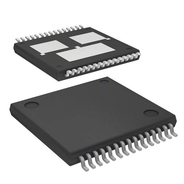


 工商网监
湘ICP备2023018690号
工商网监
湘ICP备2023018690号
