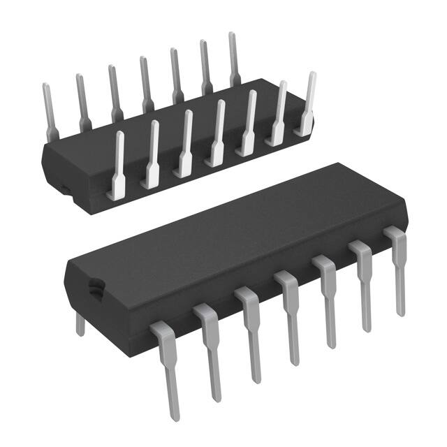
DG304B, DG306B, DG307B
Vishay Siliconix
CMOS Analog Switches
DESCRIPTION
FEATURES
The DG304B, DG306B and DG307B monolithic CMOS
switches were designed for applications in communications,
instrumentation and process control. This series is well
suited for applications requiring fast switching and nearly flat
on-resistance over the entire analog range.
•
•
•
•
•
Designed on the Vishay Siliconix PLUS-40 CMOS process
to achieve low power consumption and excellent on/off
switch performance, these switches are ideal for battery
powered applications, without sacrificing switching speed.
• Micropower: 30 nW
Break-before-make switching action is guaranteed, and an
epitaxial layer prevents latchup. Single supply operation (for
positive switch voltages) is allowed by connecting the V- rail
to 0 V.
Each switch conducts equally well in both directions when
on, and blocks up to the supply voltage when off. These
switches are CMOS input compatible.
± 15 V input range
Fast switching - tON: 110 ns
Low RDS(on): 30
Single supply operation
CMOS logic levels
BENEFITS
•
•
•
•
Full rail-to-rail analog signal range
Low signal error
Wide dynamic range
Low power dissipation
APPLICATIONS
• Low level switching circuits
• Programmable gain amplifiers
• Portable and battery powered systems
FUNCTIONAL BLOCK DIAGRAM AND PIN CONFIGURATION
NC
D1
NC
S1
NC
IN1
GND
Plastic DIP
DG306B
Plastic DIP
DG304B
V+
NC
D2
V+
1
14
S3
2
13
S4
NC
D3
3
12
D4
11
S2
D1
4
11
D2
5
10
NC
S1
5
10
S2
6
9
IN2
IN1
6
9
IN2
1
14
2
13
3
12
4
8
7
GND
V-
7
Top View
Top View
8
V-
TRUTH TABLE
TRUTH TABLE
Logic
Switch
Logic
Switch
0
OFF
0
OFF
1
ON
1
ON
Logic “0” 3.5 V
Logic “1” 11 V
Logic “0” 3.5 V
Logic “1” 11 V
* Pb containing terminations are not RoHS compliant, exemptions may apply.
Document Number: 71403
S11-0303-Rev. D, 28-Feb-11
www.vishay.com
1
�DG304B, DG306B, DG307B
Vishay Siliconix
FUNCTIONAL BLOCK DIAGRAM AND PIN CONFIGURATION
Plastic DIP
DG307B
NC
V+
1
14
S3
2
13
S4
D3
3
12
D4
D1
4
11
D2
S1
5
10
S2
IN1
6
9
IN2
GND
7
Top View
V-
8
Four SPST switches per package
TRUTH TABLE
Logic
SW1, SW2
SW3, SW4
0
OFF
ON
1
ON
OFF
Logic “0” 3.5 V
Logic “1” 11 V
ORDERING INFORMATION
Temp. Range
- 40 °C to 85 °C
Package
14-Pin Plastic DIP
Standard Part Number
Lead (Pb)-free Part Number
DG304BDJ
DG304BDJ-E3
DG306BDJ
DG306BDJ-E3
DG307BDJ
DG307BDJ-E3
ABSOLUTE MAXIMUM RATINGS (TA = 25 °C, unless otherwise noted)
Parameter
Limit
Voltages Referenced V+ to V-
25
(V-) - 2 to (V+) + 2
or 30 mA, whichever occurs first
30
GND
Digital Inputs
a,
VS, VD
Current (Any Terminal)
Continuous Current, S or D (Pulsed at 1 ms, 10 % duty cycle max.)
Storage Temperature
Power Dissipationb
Unit
44
14-Pin Plastic DIPc
100
V
mA
- 65 to 150
°C
470
mW
Notes:
a. Signals on SX, DX, or INX exceeding V+ or V- will be clamped by internal diodes. Limit forward diode current to maximum current ratings.
b. All leads welded or soldered to PC board.
c. Derate 11 mW/°C above 25 °C.
www.vishay.com
2
Document Number: 71403
S11-0303-Rev. D, 28-Feb-11
�DG304B, DG306B, DG307B
Vishay Siliconix
SPECIFICATIONSa
Parameter
Symbol
Test Conditions
Unless Otherwise Specified
V+ = 15 V, V- = - 15 V
VIN = 3.5 V or 11 Vf
Limits
- 40 °C to 85 °C
Temp.b
Min.d
Full
- 15
Typ.c
Max.d
Unit
15
V
30
50
75
5
100
5
100
5
200
Analog Switch
Analog Signal Rangee
VANALOG
Drain-Source On-Resistance
RDS(on)
Source Off Leakage Current
IS(off)
VD = ± 10 V, IS = 10 mA
VS = ± 14 V, VD = ± 14 V
Drain Off Leakage Current
ID(off)
Drain On Leakage Current
ID(on)
VD = VS = ± 14 V
Room
Full
Room
Full
Room
Full
Room
Full
-5
- 100
-5
- 100
-5
- 200
± 0.1
± 0.1
± 0.1
nA
Digital Control
IINH
Input Current with
Input Voltage Low
IINL
VIN = 15 V
Dynamic Characteristics
Turn-On Time
tON
Turn-Off Time
tOFF
Break-Before-Make Time
Charge Injection
tOPEN
Q
Source-Off Capacitance
CS(off)
Drain-Off Capacitance
CD(off)
Channel-On Capacitance
CD(on)
Input Capacitance
Off-Isolation
Crosstalk (Channel-to-Channel)
Room
Full
Room
Full
Room
Full
VIN = 5 V
Input Current with
Input Voltage High
CIN
OIRR
XTALK
VIN = 0 V
DG305A/307A ONLY, see figure 3
CL = 1 nF, Rgen = 0 , Vgen = 0 V
see figure 4
VS, VD = 0 V, f = 1 MHz
VIN = 0 V
VIN = 15 V
VIN = 0 V, RL = 1 k
VS = 1 Vrms, f = 500 kHz
- 0.001
0.001
-1
Room
see figure 2
f = 1 MHz
-1
1
µA
- 0.001
110
Room
70
Room
50
Room
30
Room
14
Room
14
Room
40
Room
6
Room
7
Room
62
Room
74
Room
Full
Room
Full
0.001
ns
pC
pF
dB
Power Supplies
Positive Supply Current
I+
Negative Supply Current
I-
VIN = 15 V or 0 V
(all inputs)
- 100
100
µA
- 0.001
Notes:
a. Refer to PROCESS OPTION FLOWCHART.
b. Room = 25 °C, Full = as determined by the operating temperature suffix.
c. Typical values are for DESIGN AID ONLY, not guaranteed nor subject to production testing.
d. The algebraic convention whereby the most negative value is a minimum and the most positive a maximum, is used in this data sheet.
e. Guaranteed by design, not subject to production test.
f. VIN = input voltage to perform proper function.
Stresses beyond those listed under “Absolute Maximum Ratings” may cause permanent damage to the device. These are stress ratings only, and functional operation
of the device at these or any other conditions beyond those indicated in the operational sections of the specifications is not implied. Exposure to absolute maximum
rating conditions for extended periods may affect device reliability.
Document Number: 71403
S11-0303-Rev. D, 28-Feb-11
www.vishay.com
3
�DG304B, DG306B, DG307B
Vishay Siliconix
TYPICAL CHARACTERISTICS (25 °C, unless otherwise noted)
TA = 25 °C
R DS(on) - Drain-Source On-Resistance ()
R DS(on) - Drain-Source On-Resistance ()
100
80
±5V
60
± 7.5 V
40
± 10 V
± 15 V
20
± 20 V
0
TA = 25 °C
V- = 0 V
100
+ 7.5 V
80
+ 10 V
60
+ 15 V
+ 20 V
40
20
0
- 20
- 15
- 10
-5
0
5
10
15
0
20
5
10
15
20
VD - Drain Voltage (V)
VD - Drain Voltage (V)
RDS(on) vs. VD and + Power Supply Voltage
RDS(on) vs. VD and ± Power Supply
10
10
TA = 25 °C
9
0
8
ID(off) or IS(off)
7
6
ID(on)
V T (V)
I S , ID (pA)
- 10
- 20
5
4
3
- 30
2
1
- 40
0
- 15 - 12
-9
-6
-3
0
3
6
9
12
15
5
10
15
20
VD or V S - Drain or Source Voltage (V)
V+, V- Positive and Negative Supplies (V)
Leakage Currents vs. Analog Voltage
Input Switching Threshold vs. V+ and VSupply Voltages
240
240
V- = - 15 V
TA = 25 °C
VINH = 15 V
VINL = 0 V
200
V+ = 15 V
TA = 25 °C
VINH = 15 V
VINL = 0 V
200
tON
t ON , t OFF (ns)
t ON , t OFF (ns)
0
160
120
tOFF
160
tON
120
tOFF
80
80
40
40
0
www.vishay.com
4
5
10
15
0
-5
- 10
- 15
V+ - Positive Supply Voltage (V)
V- - Negative Supply Voltage (V)
Switching Time vs. Positive Supply Voltage
Switching Time vs. Negative Supply Voltage
Document Number: 71403
S11-0303-Rev. D, 28-Feb-11
�DG304B, DG306B, DG307B
Vishay Siliconix
TYPICAL CHARACTERISTICS (25 °C, unless otherwise noted)
8
V+ = 15 V
RL =
CL = 0
VS = Open
I+, I- (mA)
6
4
2
0
1k
10 k
100 k
1M
f - Frequency (Hz)
Supply Currents vs. Toggle Frequency
SCHEMATIC DIAGRAM (Typical Channel)
V+
S
VLevel
Shift/
Drive
VIN
V+
GND
D
V-
Figure 1.
TEST CIRCUITS
+ 15 V
Logic "1" = Switch On
V+
VS = 3 V
S
Logic
Input
D
VINH
50 %
VO
0V
IN
RL
300
15 V
CL
33 pF
VS
V-
GND
90 %
10 %
0V
- 15 V
CL (includes fixture and stray capacitance)
VO = V S
Switch
Output
tON
tOFF
RL
RL + rDS(on)
Figure 2. Switching Time
Document Number: 71403
S11-0303-Rev. D, 28-Feb-11
www.vishay.com
5
�DG304B, DG306B, DG307B
Vishay Siliconix
TEST CIRCUITS
+ 15 V
V+
VS1 = 3 V
VS2 = 3 V
S1
D1
S2
D2
Switch
Output
RL1
300
V-
RL2
300
CL1
33 pF
CL2
33 pF
VINH
50 %
0V
VO1
VO2
IN
GND
Logic "1" = Switch On
Logic
Input
VS1
50 %
VO1
0V
VS2
VO2
Switch
Output
50 %
0V
tBBM
- 15 V
CL (includes fixture and stray capacitance)
Figure 3. Break-Before-Make SPDT (DG307B)
+ 15 V
Rg
V+
S
IN
Vg
VO
D
VO
VO
CL
1 nF
3V
INX
ON
V-
GND
OFF
ON
Q = VO x CL
- 15 V
Figure 4. Charge Injection
APPLICATIONS HINTSa
VS or VD
Analog Voltage
Range
(V)
0
VIN
Logic Input Voltage
VINH(min)/VINL(max)
(V)
11/3.5
0
11/3.5
- 20 to 20
0
11/3.5
0 to 15
V+
Positive Supply
Voltage
(V)
VNegative Supply
Voltage
(V)
GND
Voltage
(V)
15
- 15
20
- 20
15
0
- 15 to 15
Notes:
a. Application hints are for DESIGN AID ONLY, not guaranteed and not subject to production testing.
www.vishay.com
6
Document Number: 71403
S11-0303-Rev. D, 28-Feb-11
�DG304B, DG306B, DG307B
Vishay Siliconix
APPLICATIONS
- 15 V
10 k
VIN
10 k
VOUT
+ 15 V
- 15 V
10 k
10 k
100 k
1 M
A1
A0
DG304B
Binary
Input
Gain
11
10
01
00
1
10
100
1000
Figure 5. Low Power Binary to 10n Gain Low Frequency Amplifier
+ 15 V
+ 15 V
- 15 V
- 15 V
VIN1
VOUT
VIN2
CMOS Logic
Input Select
High = V IN1
- 15 V
+ 15 V
CMOS Logic
Gain Select
High = 10 x
10 x
1x
DG307B
GND
20 k
180 k
Figure 6. Low Power Instrumentation Amplifier with Digitally Selectable Inputs and Gain
Vishay Siliconix maintains worldwide manufacturing capability. Products may be manufactured at one of several qualified locations. Reliability data for Silicon
Technology and Package Reliability represent a composite of all qualified locations. For related documents such as package/tape drawings, part marking, and
reliability data, see www.vishay.com/ppg?71403.
Document Number: 71403
S11-0303-Rev. D, 28-Feb-11
www.vishay.com
7
�Package Information
Vishay Siliconix
PDIP: 14ĆLEAD
14
13
12
11
10
9
8
E
E1
1
2
3
4
5
6
7
D
S
Q1
A
A1
L
15°
MAX
C
B1
e1
B
Dim
A
A1
B
B1
C
D
E
E1
e1
eA
L
Q1
S
eA
MILLIMETERS
Min
Max
INCHES
Min
Max
3.81
5.08
0.150
0.200
0.38
1.27
0.015
0.050
0.38
0.51
0.015
0.020
0.89
1.65
0.035
0.065
0.20
0.30
0.008
0.012
17.27
19.30
0.680
0.760
7.62
8.26
0.300
0.325
5.59
7.11
0.220
0.280
2.29
2.79
0.090
0.110
7.37
7.87
0.290
0.310
2.79
3.81
0.110
0.150
1.27
2.03
0.050
0.080
1.02
2.03
0.040
0.080
ECN: S-03946—Rev. C, 09-Jul-01
DWG: 5481
Document Number: 71260
05-Jul-01
www.vishay.com
1
�Legal Disclaimer Notice
www.vishay.com
Vishay
Disclaimer
ALL PRODUCT, PRODUCT SPECIFICATIONS AND DATA ARE SUBJECT TO CHANGE WITHOUT NOTICE TO IMPROVE
RELIABILITY, FUNCTION OR DESIGN OR OTHERWISE.
Vishay Intertechnology, Inc., its affiliates, agents, and employees, and all persons acting on its or their behalf (collectively,
“Vishay”), disclaim any and all liability for any errors, inaccuracies or incompleteness contained in any datasheet or in any other
disclosure relating to any product.
Vishay makes no warranty, representation or guarantee regarding the suitability of the products for any particular purpose or
the continuing production of any product. To the maximum extent permitted by applicable law, Vishay disclaims (i) any and all
liability arising out of the application or use of any product, (ii) any and all liability, including without limitation special,
consequential or incidental damages, and (iii) any and all implied warranties, including warranties of fitness for particular
purpose, non-infringement and merchantability.
Statements regarding the suitability of products for certain types of applications are based on Vishay’s knowledge of typical
requirements that are often placed on Vishay products in generic applications. Such statements are not binding statements
about the suitability of products for a particular application. It is the customer’s responsibility to validate that a particular
product with the properties described in the product specification is suitable for use in a particular application. Parameters
provided in datasheets and/or specifications may vary in different applications and performance may vary over time. All
operating parameters, including typical parameters, must be validated for each customer application by the customer’s
technical experts. Product specifications do not expand or otherwise modify Vishay’s terms and conditions of purchase,
including but not limited to the warranty expressed therein.
Except as expressly indicated in writing, Vishay products are not designed for use in medical, life-saving, or life-sustaining
applications or for any other application in which the failure of the Vishay product could result in personal injury or death.
Customers using or selling Vishay products not expressly indicated for use in such applications do so at their own risk. Please
contact authorized Vishay personnel to obtain written terms and conditions regarding products designed for such applications.
No license, express or implied, by estoppel or otherwise, to any intellectual property rights is granted by this document or by
any conduct of Vishay. Product names and markings noted herein may be trademarks of their respective owners.
Material Category Policy
Vishay Intertechnology, Inc. hereby certifies that all its products that are identified as RoHS-Compliant fulfill the
definitions and restrictions defined under Directive 2011/65/EU of The European Parliament and of the Council
of June 8, 2011 on the restriction of the use of certain hazardous substances in electrical and electronic equipment
(EEE) - recast, unless otherwise specified as non-compliant.
Please note that some Vishay documentation may still make reference to RoHS Directive 2002/95/EC. We confirm that
all the products identified as being compliant to Directive 2002/95/EC conform to Directive 2011/65/EU.
Vishay Intertechnology, Inc. hereby certifies that all its products that are identified as Halogen-Free follow Halogen-Free
requirements as per JEDEC JS709A standards. Please note that some Vishay documentation may still make reference
to the IEC 61249-2-21 definition. We confirm that all the products identified as being compliant to IEC 61249-2-21
conform to JEDEC JS709A standards.
Revision: 02-Oct-12
1
Document Number: 91000
�


 工商网监
湘ICP备2023018690号
工商网监
湘ICP备2023018690号
