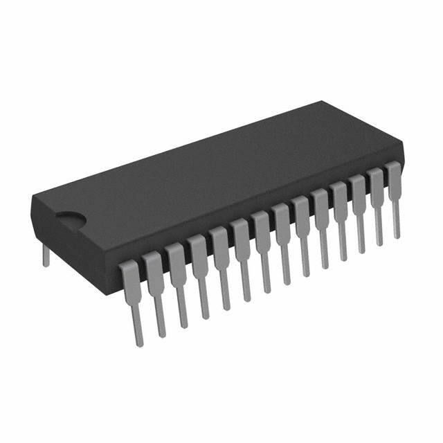
DG406B, DG407B
www.vishay.com
Vishay Siliconix
16-Ch/Dual 8-Ch High-Performance CMOS Analog Multiplexers
DESCRIPTION
FEATURES
The DG406B is a 16-channel single-ended analog
multiplexer designed to connect one of sixteen inputs to a
common output as determined by a 4-bit binary address.
The DG407B selects one of eight differential inputs to a
common differential output. Break-before-make switching
action protects against momentary shorting of inputs.
• Low on-resistance - RDS(on): 45
An on channel conducts current equally well in both
directions. In the off state each channel blocks voltages up
to the power supply rails. An enable (EN) function allows the
user to reset the multiplexer/demultiplexer to all switches off
for stacking several devices. All control inputs, address (Ax)
and enable (EN) are TTL compatible over the full specified
operating temperature range.
• Material categorization: For definitions of compliance
please see www.vishay.com/doc?99912
Applications for the DG406B, DG407B include high speed
data acquisition, audio signal switching and routing, ATE
systems, and avionics. High performance and low power
dissipation make them ideal for battery operated and
remote instrumentation applications.
Designed in the 44 V silicon-gate CMOS process, the
absolute maximum voltage rating is extended to 44 V,
allowing operation with ± 20 V supplies. Additionally
single (12 V) supply operation is allowed. An epitaxial layer
prevents latchup.
• Low charge injection - Q: 11 pC
Available
• Fast transition time - tTRANS: 115 ns
Available
• Low power: 0.2 mW
• Single supply capability
Note
* This datasheet provides information about parts that are
RoHS-compliant and/or parts that are non-RoHS-compliant. For
example, parts with lead (Pb) terminations are not RoHS-compliant.
Please see the information/tables in this datasheet for details.
BENEFITS
•
•
•
•
•
•
Higher accuracy
Reduced glitching
Improved data throughput
Reduced power consumption
Increased ruggedness
Wide supply ranges: ± 5 V to ± 20 V
APPLICATIONS
•
•
•
•
•
•
•
Data acquisition systems
Audio signal routing
Medical instrumentation
ATE systems
Battery powered systems
High-rel systems
Single supply systems
FUNCTIONAL BLOCK DIAGRAM AND PIN CONFIGURATION
DG406B
DG407B
Dual-In-Line and SOIC Wide-Body
V+
1
28
Da
V-
Db
2
27
V-
26
S8
NC
3
26
S8a
25
S7
S8b
4
25
S7a
5
24
S6a
V+
1
28
D
NC
2
27
NC
S16
3
4
Dual-In-Line and SOIC Wide-Body
S15
5
24
S6
S7b
S14
6
23
S5
S6b
6
23
S5a
22
S4
S5b
7
22
S4a
21
S3
S4b
8
21
S3a
S13
S12
7
8
S11
9
20
S2
S3b
9
20
S2a
S10
10
19
S1
S2b
10
19
S1a
18
EN
S1b
11
18
EN
17
A0
S9
11
GND
12
17
A0
GND
12
NC
13
16
A1
NC
13
A3
14
15
A2
NC
Decoders/Drivers
Top View
S13-2513-Rev. D, 09-Dec-13
Decoders/Drivers
14
16
A1
15
A2
Top View
Document Number: 72552
1
For technical questions, contact: analogswitchtechsupport@vishay.com
THIS DOCUMENT IS SUBJECT TO CHANGE WITHOUT NOTICE. THE PRODUCTS DESCRIBED HEREIN AND THIS DOCUMENT
ARE SUBJECT TO SPECIFIC DISCLAIMERS, SET FORTH AT www.vishay.com/doc?91000
�DG406B, DG407B
www.vishay.com
Vishay Siliconix
FUNCTIONAL BLOCK DIAGRAM AND PIN CONFIGURATION
S15
Da
V-
V+
D
28 27 26
Db
V+
1
NC
NC
2
S 8b
NC
3
S8
S 16
4
S 8a
PLCC and LCC
DG407B
4
3
2
1
28 27 26
V-
PLCC and LCC
DG406B
5
25
S7
S7b
5
25
S7a
S14
6
24
S6
S6b
6
24
S6a
S13
7
23
S5
S5b
7
23
S5a
S4b
8
22
S4a
22
S11
9
21
S3
S3b
9
21
S3a
20
S2
S2b
10
20
S2a
19
S1
S1b
11
19
S1a
EN
A0
A1
A2
NC
12 13 14 15 16 17 18
NC
12 13 14 15 16 17 18
EN
Decoders/Drivers
A0
Decoders/Drivers
A1
11
A2
S9
A3
10
NC
S10
GND
8
S4
GND
S12
Top View
Top View
TRUTH TABLE (DG406B)
TRUTH TABLE (DG407B)
A3
A2
A1
A0
EN
ON SWITCH
A2
A1
A0
EN
ON SWITCH
X
X
X
X
0
None
X
X
X
0
None
0
0
0
0
1
1
0
0
0
1
1
0
0
0
1
1
2
0
0
1
1
2
0
0
1
0
1
3
0
1
0
1
3
0
0
1
1
1
4
0
1
1
1
4
0
1
0
0
1
5
1
0
0
1
5
0
1
0
1
1
6
1
0
1
1
6
0
1
1
0
1
7
1
1
0
1
7
0
1
1
1
1
8
1
1
1
1
8
1
0
0
0
1
9
1
0
0
1
1
10
1
0
1
0
1
11
1
0
1
1
1
12
1
1
0
0
1
13
1
1
0
1
1
14
1
1
1
0
1
15
1
1
1
1
1
16
Notes
• Logic “0” = VAL 0.8 V
• Logic “1” = VAH 2.4 V
• X = Do not care
ORDERING INFORMATION (DG406B)
ORDERING INFORMATION (DG407B)
TEMP. RANGE
TEMP. RANGE
-40 °C to 85 °C
PACKAGE
PART NUMBER
28-Pin Plastic DIP
DG406BDJ,
DG406BDJ-E3
28-Pin PLCC
DG406BDN,
DG406BDN-T1-E3
28-Pin Widebody
SOIC
DG406BDW,
DG406BDW-E3,
DG406BDW-T1-E3
-40 °C to 85 °C
PACKAGE
PART NUMBER
28-Pin Plastic DIP
DG407BDJ,
DG407BDJ-E3
28-Pin PLCC
DG407BDN,
DG407BDN-T1-E3
28-Pin Widebody
SOIC
DG407BDW,
DG407BDW-E3,
DG407BDW-T1-E3
Note
• -T1 indicates Tape and Reel, -E3 indicates Lead-Free and RoHS Compliant, NO -E3 indicates standard Tin/Lead finish.
S13-2513-Rev. D, 09-Dec-13
Document Number: 72552
2
For technical questions, contact: analogswitchtechsupport@vishay.com
THIS DOCUMENT IS SUBJECT TO CHANGE WITHOUT NOTICE. THE PRODUCTS DESCRIBED HEREIN AND THIS DOCUMENT
ARE SUBJECT TO SPECIFIC DISCLAIMERS, SET FORTH AT www.vishay.com/doc?91000
�DG406B, DG407B
www.vishay.com
Vishay Siliconix
ABSOLUTE MAXIMUM RATINGS
PARAMETER
LIMIT
44
V+ to V-g
Voltages Referenced to V-
GND to V-
UNIT
-25
V
(V-) - 2 to (V+) + 2 or 20 mA,
whichever occurs first
Digital Inputsa, VS, VD
Current (any terminal)
30
Peak Current, S or D (pulsed at 1 ms, 10 % duty cycle max.)
100
Storage Temperature
Power Dissipation (Package)b
mA
-65 to 150
°C
28-Pin Plastic DIPc
625
mW
28-Pin Plastic PLCCc
450
mW
28-Pin Widebody SOICf
450
mW
Notes
a. Signals on SX, DX or INX exceeding V+ or V- will be clamped by internal diodes. Limit forward diode current to maximum current ratings.
b. All leads soldered or welded to PC board.
c. Derate 8.3 mW/°C above 75 °C.
d. Derate 16 mW/°C above 75 °C.
e. Derate 18 mW/°C above 75 °C.
f. Derate 6 mW/°C above 75 °C.
g. Also applies when V- = GND.
SPECIFICATIONS
PARAMETER
SYMBOL
TEST CONDITIONS
UNLESS OTHERWISE
SPECIFIED
TEMP.b
TYP.c
V+ = 15 V, V- = -15 V
VAL = 0.8 V, VAH = 2.4 Vf
D SUFFIX
-40 °C to 85 °C
UNIT
MIN.d
MAX.d
Analog Switch
Analog Signal Rangee
Drain-Source
On-Resistance
RDS(on) Matching Between
Channelsg
Source Off Leakage Current
VANALOG
-15
15
V
-
60
VD = ± 10 V, IS = -10 mA
sequence each switch on
Full
45
-
74
RDS(on)
VD = ± 10 V
Room
5
-
-
IS(off)
VS = ± 10 V,
VD = ± 10 V, VEN = 0 V
Room
-
-0.5
0.5
Full
-
-5
5
ID(off)
VD = ± 10 V,
VS = ± 10 V,
VEN = 0 V
DG407B
DG406B
Drain On Leakage
Current
45
RDS(on)
DG406B
Drain Off Leakage
Current
Full
Room
ID(on)
DG407B
VS = VD = ± 10 V
sequence each
switch on
Room
-
-1
1
Full
-
-40
40
Room
-
-1
1
Full
-
-20
20
Room
-
-1
1
Full
-
-40
40
Room
-
-1
1
Full
-
-20
20
%
nA
Digital Control
Logic High Input Voltage
VINH
Full
-
2.4
-
Logic Low Input Voltage
VINL
Full
-
-
0.8
Logic High Input Current
IAH
VA = 2.4 V, 15 V
Full
-
-1
1
Logic Low Input Current
IAL
VEN = 0 V, 2.4 V, VA = 0 V
Full
-
-1
1
Logic Input Capacitance
Cin
f = 1 MHz
Room
6
-
-
S13-2513-Rev. D, 09-Dec-13
V
μA
pF
Document Number: 72552
3
For technical questions, contact: analogswitchtechsupport@vishay.com
THIS DOCUMENT IS SUBJECT TO CHANGE WITHOUT NOTICE. THE PRODUCTS DESCRIBED HEREIN AND THIS DOCUMENT
ARE SUBJECT TO SPECIFIC DISCLAIMERS, SET FORTH AT www.vishay.com/doc?91000
�DG406B, DG407B
www.vishay.com
Vishay Siliconix
SPECIFICATIONS
PARAMETER
SYMBOL
TEST CONDITIONS
UNLESS OTHERWISE
SPECIFIED
TEMP.b
TYP.c
V+ = 15 V, V- = -15 V
D SUFFIX
-40 °C to 85 °C
UNIT
MIN.d
VAL = 0.8 V, VAH = 2.4 Vf
MAX.d
Dynamic Characteristics
Transition Time
tTRANS
see figure 2
Break-Before-Make Interval
tOPEN
see figure 4
Enable Turn-On Time
tON(EN)
see figure 3
Enable Turn-Off Time
tOFF(EN)
Room
115
-
148
Full
-
-
161
Room
39
10
-
Full
-
21
-
Room
75
-
107
123
Full
-
-
Room
50
-
88
Full
-
-
94
ns
Q
CL = 1 nF, VS = 0 V
RS = 0
Room
11
-
-
pC
Off Isolationh
OIRR
VEN = 0 V, RL = 50 ,
f = 1 MHz
Room
-86
-
-
dB
Source Off Capacitance
CS(off)
VEN = 0 V, VS = 0 V,
f = 1 MHz
Room
6
-
-
Drain Off
Capacitance
Room
108
-
-
DG407B
CD(off)
Room
54
-
-
Drain On
Capacitance
DG407B
Charge Injection
DG406B
CD(on)
VEN = 0 V,
VD = 0 V,
f = 1 MHz
Room
114
-
-
Room
57
-
-
Room
23
-
30
Full
-
-
75
Room
-0.02
-1
-
Full
-
-10
-
Room
28
-
500
pF
Power Supplies
Positive Supply Current
I+
Negative Supply Current
I-
Positive Supply Current
I+
VEN = VA = 0 V or 5 V
VEN = 2.4 V, VA = 0 V
Negative Supply Current
I-
Full
-
-
700
Room
-0.01
-20
-
Full
-
-20
-
μA
Notes
a. Guaranteed by ± 15 V leakage test, not production tested.
b. Room = 25 °C, Full = as determined by the operating temperature suffix.
c. Typical values are for DESIGN AID ONLY, not guaranteed nor subject to production testing.
d. The algebraic convention whereby the most negative value is a minimum and the most positive a maximum, is used in this datasheet.
e. Guaranteed by design, not subject to production test.
f. VIN = input voltage to perform proper function.
g. RDS(on) = RDS(on) max. - RDS(on) min.
h. Worst case isolation occurs on channel 4 due to proximity to the drain pin.
S13-2513-Rev. D, 09-Dec-13
Document Number: 72552
4
For technical questions, contact: analogswitchtechsupport@vishay.com
THIS DOCUMENT IS SUBJECT TO CHANGE WITHOUT NOTICE. THE PRODUCTS DESCRIBED HEREIN AND THIS DOCUMENT
ARE SUBJECT TO SPECIFIC DISCLAIMERS, SET FORTH AT www.vishay.com/doc?91000
�DG406B, DG407B
www.vishay.com
Vishay Siliconix
SPECIFICATIONS FOR SINGLE SUPPLY
PARAMETER
SYMBOL
TEST CONDITIONS
UNLESS OTHERWISE
SPECIFIED
TEMP.b
TYP.c
V+ = 15 V, V- = -15 V
D SUFFIX
-40 °C to 85 °C
UNIT
MIN.d
VAL = 0.8 V, VAH = 2.4 Vf
MAX.d
Analog Switch
Analog Signal Rangee
Drain-Source On-Resistance
RDS(on) Matching Between
Channelsg
Source Off Leakage Currenta
Drain Off Leakage
Current
DG406B
Drain On Leakage
Current
DG406B
DG407B
VANALOG
Full
-
0
12
V
RDS(on)
Room
78
-
100
Room
5
-
-
%
Room
-
-0.5
0.5
Room
-
-1
1
Room
-
-1
1
Room
-
-1
1
Room
-
-1
1
Room
130
-
163
Room
93
-
125
Room
63
-
94
Room
9
-
-
Room
13
-
30
Full
-
-
75
Room
-0.01
-20
-
Full
-
-20
-
RDS(on)
IS(off)
ID(off)
VD = 3 V, IS = -1 mA
sequence each switch on
VD = 10 V or 0.5 V,
VS = 0.5 V or 10 V,
VEN = 0 V
ID(on)
VS = VD = ± 10 V
sequence each switch on
Transition Time
tTRANS
VS1 = 8 V, VS8 = 0 V,
VIN = 2.4 V
Enable Turn-On Time
tON(EN)
Enable Turn-Off Time
tOFF(EN)
DG407B
nA
Dynamic Characteristics
Charge Injection
Q
VINH = 2.4 V, VINL = 0 V,
VIN = 5 V
CL = 1 nF, VS = 6 V
RS = 0
ns
pC
Power Supplies
Positive Supply Current
Positive Supply Current
I+
I+
VEN = 0 V or 5 V
VA = 0 V or 5 V
μA
Notes
a. Guaranteed by ± 15 V leakage test, not production tested.
b. Room = 25 °C, Full = as determined by the operating temperature suffix.
c. Typical values are for DESIGN AID ONLY, not guaranteed nor subject to production testing.
d. The algebraic convention whereby the most negative value is a minimum and the most positive a maximum, is used in this datasheet.
e. Guaranteed by design, not subject to production test.
f. VIN = input voltage to perform proper function.
g. RDS(on) = RDS(on) max. - RDS(on) min.
h. Worst case isolation occurs on channel 4 due to proximity to the drain pin.
Stresses beyond those listed under “Absolute Maximum Ratings” may cause permanent damage to the device. These are stress ratings only, and functional operation
of the device at these or any other conditions beyond those indicated in the operational sections of the specifications is not implied. Exposure to absolute maximum
rating conditions for extended periods may affect device reliability.
S13-2513-Rev. D, 09-Dec-13
Document Number: 72552
5
For technical questions, contact: analogswitchtechsupport@vishay.com
THIS DOCUMENT IS SUBJECT TO CHANGE WITHOUT NOTICE. THE PRODUCTS DESCRIBED HEREIN AND THIS DOCUMENT
ARE SUBJECT TO SPECIFIC DISCLAIMERS, SET FORTH AT www.vishay.com/doc?91000
�DG406B, DG407B
www.vishay.com
Vishay Siliconix
TYPICAL CHARACTERISTICS (TA = 25 °C, unless otherwise noted)
350
TA = 25 °C
105
±5V
85
±8V
65
± 10 V
± 12 V
± 15 V
± 20 V
45
25
5
- 20
R DS(on) - Drain-Source On-Resistance (Ω)
R DS(on) - Drain-Source On-Resistance ()
125
TA = 25 °C
300
V+ = 5.0 V
250
V+ = 10 V
200
V+ = 12 V
150
V+ = 15 V
100
V+ = 20 V
V+ = 22 V
50
0
- 15
- 10
-5
0
5
10
15
0
20
2
4
6
10
12
16
18
20
22
On-Resistance vs. VD and Unipolar Supply Voltage
85
145
V ± = ± 15 V
75
85 °C
65
125 °C
55
45
25 °C
35
- 55 °C
25
15
5
- 15
85 °C
125
125 °C
105
85
25 °C
65
- 55 °C
45
V+ = 12 V
V- = 0 V
25
5
- 10
-5
0
5
10
15
0
2
4
VD - Drain Voltage (V)
8
10
12
On-Resistance vs. VD and Temperature
200
150
6
VD - Drain Voltage (V)
On-Resistance vs. VD and Temperature
10000
V- = - 15 V
TA = 25 °C
V ± = ± 15 V
1000
100
IS(off)
ID(on)
ID(off)
50
Leakage (pA)
ID, IS (pA)
14
On-Resistance vs. VD and Dual Supply Voltage
R DS(on) - Drain-Source On-Resistance ()
R DS(on) - Drain-Source On-Resistance (Ω)
8
VD - Drain Voltage (V)
VD - Drain Voltage (V)
0
IS(off)
- 50
100
ID(on)
ID(off)
10
- 100
- 150
- 200
- 15
- 10
-5
0
5
10
VD or V S - Drain or Source Voltage (V)
Leakage vs. Analog Voltage
S13-2513-Rev. D, 09-Dec-13
15
1
- 80 - 60 - 40 - 20
0
20
40
60
80 100 120 140
Temperature (°C)
Leakage vs. Current
Document Number: 72552
6
For technical questions, contact: analogswitchtechsupport@vishay.com
THIS DOCUMENT IS SUBJECT TO CHANGE WITHOUT NOTICE. THE PRODUCTS DESCRIBED HEREIN AND THIS DOCUMENT
ARE SUBJECT TO SPECIFIC DISCLAIMERS, SET FORTH AT www.vishay.com/doc?91000
�DG406B, DG407B
www.vishay.com
Vishay Siliconix
TYPICAL CHARACTERISTICS (TA = 25 °C, unless otherwise noted)
200
100 m
V ± = ± 15 V
175
1m
150
I+
100 µ
Time (ns)
I+ - Supply Current (nA)
10 m
10 µ
1µ
I-
tTRANS
125
100
tON(en)
100 n
75
tOFF(en)
10 n
50
1n
25
100 p
10
100
1K
10 K
100 K
1M
10 M
±5
± 10
Input Switching Frequency (Hz)
± 15
± 20
Supply Voltage (V)
Supply Current vs. Input Switching Frequency
Switching Time vs. Bipolar Supplies
3.0
300
275
2.5
VT - Switching Threshold (V)
250
225
Time (ns)
200
tTRANS
175
150
125
tOFF(en)
tON(en)
100
75
2.0
1.5
1.0
0.5
50
0.0
25
5
10
15
5
20
10
Supply Voltage (V)
15
20
25
30
V+ - Supply Voltage (V)
Switching Time vs. Single Supplies
Switching Threshold vs. Supply Voltage
35
10
30
C = 1 nF
25
- 10
Q - Charge Injection (pC)
Loss, OIRR, X TALK (dB)
20
Loss
- 30
- 50
OIRR
- 70
XTALK
V+ = 15 V
V - = - 15 V
RL = 50 Ω
- 90
1M
10 M
Frequency (Hz)
100 M
V=5V
5
0
V+ = 12 V
-5
- 10
- 15
- 20
V = 15 V
- 30
1G
Insertion Loss, Off -Isolation Crosstalk vs. Frequency
S13-2513-Rev. D, 09-Dec-13
10
- 25
- 110
100 k
15
- 35
- 15 - 12
-9
-6
-3
0
3
6
9
12
15
VS - Analog Voltage (V)
Charge Injection vs. Analog Voltage
Document Number: 72552
7
For technical questions, contact: analogswitchtechsupport@vishay.com
THIS DOCUMENT IS SUBJECT TO CHANGE WITHOUT NOTICE. THE PRODUCTS DESCRIBED HEREIN AND THIS DOCUMENT
ARE SUBJECT TO SPECIFIC DISCLAIMERS, SET FORTH AT www.vishay.com/doc?91000
�DG406B, DG407B
www.vishay.com
Vishay Siliconix
TYPICAL CHARACTERISTICS (TA = 25 °C, unless otherwise noted)
200
175
Time (ns)
150
tTRANS V = ± 15 V
125
100
tON V = ± 15 V
75
tOFF V = ± 15 V
50
25
- 55 - 35
- 15
5
25
45
65
85
105
125
Temperature (°C)
Switching Time vs. Temperature
SCHEMATIC DIAGRAM (Typical Channel)
V+
GND
VREF
D
A0
V+
Level
Shift
AX
Decode/
Drive
V-
S1
V+
EN
Sn
V-
Fig. 1
S13-2513-Rev. D, 09-Dec-13
Document Number: 72552
8
For technical questions, contact: analogswitchtechsupport@vishay.com
THIS DOCUMENT IS SUBJECT TO CHANGE WITHOUT NOTICE. THE PRODUCTS DESCRIBED HEREIN AND THIS DOCUMENT
ARE SUBJECT TO SPECIFIC DISCLAIMERS, SET FORTH AT www.vishay.com/doc?91000
�DG406B, DG407B
www.vishay.com
Vishay Siliconix
TEST CIRCUITS
+ 15 V
+ 2.4 V
V+
EN
A2
A1
± 10 V
S1
A3
S2 - S15
DG406B
S16
A0
± 10 V
GND
Logic
Input
VO
D
V-
tr < 5 ns
tf < 5 ns
3V
50 %
0V
50 Ω
35 pF
300 Ω
- 15 V
VS1
90 %
Switch
Output
+ 15 V
+ 2.4 V
V+
EN
A2
VO
S1b
0V
90 %
10 V
VS8
*
DG407B
S8b
A1
A0
tTRANS
10 V
S1 ON
Db
GND
tTRANS
S8 ON
VO
V-
50 Ω
35 pF
300 Ω
- 15 V
* = S1a – S 8a, S2b - S7b, Da
Fig. 2 - Transition Time
+ 15 V
V+
A3
S1
A2
A1
A0
-5V
S2 - S16
DG406B
EN
VO
D
GND
V300 Ω
50 Ω
Logic
Input
35 pF
- 15 V
tr < 5 ns
tf < 5 ns
3V
50 %
0V
tON(EN)
0V
+ 15 V
V+
A2
S1b
S1a - S8a
S2b - S8b
A1
A0
tOFF(EN)
Switch
Output
- 5V
VO
90 %
90 %
VO
DG407B
Da and Db
EN
GND
VO
V-
50 Ω
35 pF
300 Ω
- 15 V
Fig. 3 - Enable Switching Time
S13-2513-Rev. D, 09-Dec-13
Document Number: 72552
9
For technical questions, contact: analogswitchtechsupport@vishay.com
THIS DOCUMENT IS SUBJECT TO CHANGE WITHOUT NOTICE. THE PRODUCTS DESCRIBED HEREIN AND THIS DOCUMENT
ARE SUBJECT TO SPECIFIC DISCLAIMERS, SET FORTH AT www.vishay.com/doc?91000
�DG406B, DG407B
www.vishay.com
Vishay Siliconix
TEST CIRCUITS
+ 15 V
Logic
Input
V+
EN
+ 2.4 V
All S and Da
A3
A2
A1
+5V
tr < 5 ns
tf < 5 ns
3V
50 %
0V
DG406B
DG407B
A0
GND
50 Ω
VS
VO
D,D b
80 %
Switch
Output
V300 Ω
35 pF
VO
- 15 V
0V
tOPEN
Fig. 4 - Break-Before-Make Interval
Vishay Siliconix maintains worldwide manufacturing capability. Products may be manufactured at one of several qualified locations. Reliability data for Silicon
Technology and Package Reliability represent a composite of all qualified locations. For related documents such as package/tape drawings, part marking, and
reliability data, see www.vishay.com/ppg?72552.
S13-2513-Rev. D, 09-Dec-13
Document Number: 72552
10
For technical questions, contact: analogswitchtechsupport@vishay.com
THIS DOCUMENT IS SUBJECT TO CHANGE WITHOUT NOTICE. THE PRODUCTS DESCRIBED HEREIN AND THIS DOCUMENT
ARE SUBJECT TO SPECIFIC DISCLAIMERS, SET FORTH AT www.vishay.com/doc?91000
�Package Information
Vishay Siliconix
PDIP: 28ĆLEAD
28
27
26
25
24
23
22
21
20
19
18
17
16
15
E1
1
2
3
4
5
6
7
8
9
10
11
12
13
E
14
D
Q1
S
A(1)
A
L
A1
L
15°
MAX.
C
e1
B1
Dim
A
A1
B
B1
C
D
E
E1
e1
eA
L
Q1
S
eA
B
MILLIMETERS
Min
Max
INCHES
Min
Max
2.29
5.08
0.090
0.200
0.39
1.77
0.015
0.070
0.38
0.56
0.015
0.022
0.89
1.65
0.035
0.065
0.204
0.30
0.008
0.012
35.10
39.70
1.380
1.565
15.24
15.88
0.600
0.625
13.21
14.73
0.520
0.580
2.29
2.79
0.090
0.110
14.99
15.49
0.590
0.610
2.60
5.08
0.100
0.200
0.95
2.345
0.0375
0.0925
0.995
2.665
0.0375
0.105
ECN: S-03946—Rev. F, 09-Jul-01
DWG: 5488
Document Number: 71243
06-Jul-01
www.vishay.com
1
�Package Information
Vishay Siliconix
PLCC: 28-LEAD
D-SQUARE
MILLIMETERS
MIN.
MAX.
A
4.20
4.57
2.29
3.04
A1
0.51
A2
B
0.331
0.553
0.661
0.812
B1
D
12.32
12.57
11.430
11.582
D1
9.91
10.92
D2
1.27 BSC
e1
ECN: T09-0766-Rev. D, 28-Sep-09
DWG: 5491
DIM.
A2
INCHES
MIN.
MAX.
0.165
0.180
0.090
0.120
0.020
0.013
0.021
0.026
0.032
0.485
0.495
0.450
0.456
0.390
0.430
0.050 BSC
e1
B1
D2
B
D1-SQUARE
A1
D
A
Document Number: 71264
28-Sep-09
0.101 mm
0.004"
www.vishay.com
1
�Package Information
www.vishay.com
Vishay Siliconix
SOIC (WIDE-BODY): 28-LEADS
0.06 0.002D
CAVITY NO.
0.3525 0.001
0.334 0.005
28 27
26 25 24 23 22 21
20 19
18
R0.004
17 16 15
0.010
0.1475 0.001
R0.008
0.295 0.001
R0.009
1
2 3
4
5
6
7
8
9
10
11
12 13 14
4°
R0.004
2°
0.032 0.005
0.070 0.005
0.055 0.005
DETAIL A
PIN 1 INDICATOR
0.047 0.007 0.001 dp
SURFACE POLISHED
0.334 0.005
0.291 0.001
0.091 0.001
0.020 45°
0.705 0.001
0.098 0.002
R0.004
0.00825 ± 0.00325
0.041 0.001
0.050 TYP.
0.017 0.0003
7°(4 )
0.295 0.001
0.406 0.004
DETAIL A
All Dimensions In Inches
ECN: E11-2209-Rev. D, 01-Aug-11
DWG: 5850
Revision: 01-Aug-11
1
Document Number: 71268
THIS DOCUMENT IS SUBJECT TO CHANGE WITHOUT NOTICE. THE PRODUCTS DESCRIBED HEREIN AND THIS DOCUMENT
ARE SUBJECT TO SPECIFIC DISCLAIMERS, SET FORTH AT www.vishay.com/doc?91000
�Legal Disclaimer Notice
www.vishay.com
Vishay
Disclaimer
ALL PRODUCT, PRODUCT SPECIFICATIONS AND DATA ARE SUBJECT TO CHANGE WITHOUT NOTICE TO IMPROVE
RELIABILITY, FUNCTION OR DESIGN OR OTHERWISE.
Vishay Intertechnology, Inc., its affiliates, agents, and employees, and all persons acting on its or their behalf (collectively,
“Vishay”), disclaim any and all liability for any errors, inaccuracies or incompleteness contained in any datasheet or in any other
disclosure relating to any product.
Vishay makes no warranty, representation or guarantee regarding the suitability of the products for any particular purpose or
the continuing production of any product. To the maximum extent permitted by applicable law, Vishay disclaims (i) any and all
liability arising out of the application or use of any product, (ii) any and all liability, including without limitation special,
consequential or incidental damages, and (iii) any and all implied warranties, including warranties of fitness for particular
purpose, non-infringement and merchantability.
Statements regarding the suitability of products for certain types of applications are based on Vishay’s knowledge of
typical requirements that are often placed on Vishay products in generic applications. Such statements are not binding
statements about the suitability of products for a particular application. It is the customer’s responsibility to validate that a
particular product with the properties described in the product specification is suitable for use in a particular application.
Parameters provided in datasheets and / or specifications may vary in different applications and performance may vary over
time. All operating parameters, including typical parameters, must be validated for each customer application by the customer’s
technical experts. Product specifications do not expand or otherwise modify Vishay’s terms and conditions of purchase,
including but not limited to the warranty expressed therein.
Except as expressly indicated in writing, Vishay products are not designed for use in medical, life-saving, or life-sustaining
applications or for any other application in which the failure of the Vishay product could result in personal injury or death.
Customers using or selling Vishay products not expressly indicated for use in such applications do so at their own risk.
Please contact authorized Vishay personnel to obtain written terms and conditions regarding products designed for
such applications.
No license, express or implied, by estoppel or otherwise, to any intellectual property rights is granted by this document
or by any conduct of Vishay. Product names and markings noted herein may be trademarks of their respective owners.
© 2017 VISHAY INTERTECHNOLOGY, INC. ALL RIGHTS RESERVED
Revision: 08-Feb-17
1
Document Number: 91000
�


 工商网监
湘ICP备2023018690号
工商网监
湘ICP备2023018690号
