SQS966ENW
www.vishay.com
Vishay Siliconix
Automotive Dual N-Channel 60 V (D-S) 175 °C MOSFET
FEATURES
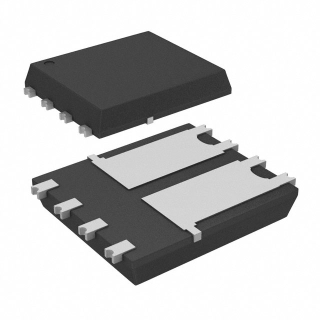
PowerPAK® 1212-8W Dual
• TrenchFET® power MOSFET
D1
D1
D2 7 8
D2 6
5
3.
3
• AEC-Q101 qualified
• 100 % Rg and UIS tested
1
2
3 G S1
4 S 1
G2 2
m
m
1
3.3
mm
Top View
• Material categorization:
for definitions of compliance please see
www.vishay.com/doc?99912
D1
D2
Bottom View
Marking code: Q027
PRODUCT SUMMARY
G1
VDS (V)
RDS(on) () at VGS = 10 V
0.036
RDS(on) () at VGS = 4.5 V
0.048
ID (A)
S1
6
Configuration
Package
G2
60
Dual
S2
N-Channel MOSFET
N-Channel MOSFET
PowerPAK 1212-8W
ABSOLUTE MAXIMUM RATINGS (TC = 25 °C, unless otherwise noted)
PARAMETER
SYMBOL
LIMIT
Drain-source voltage
VDS
60
Gate-source voltage
VGS
± 20
Continuous drain current a
TC = 25 °C
TC = 125 °C
Continuous source current (diode conduction) a
Pulsed drain current b
Single pulse avalanche current
Single pulse avalanche energy
Maximum power dissipation b
L = 0.1 mH
TC = 25 °C
TC = 125 °C
Operating junction and storage temperature range
ID
6
6
IDM
24
IAS
12
EAS
7.2
TJ, Tstg
Soldering recommendations (peak temperature) e, f
V
6
IS
PD
UNIT
27.8
9.25
-55 to +175
260
A
mJ
W
°C
THERMAL RESISTANCE RATINGS
PARAMETER
Junction-to-ambient
Junction-to-case (drain)
PCB mount c
SYMBOL
LIMIT
RthJA
94
RthJC
5.4
UNIT
°C/W
Notes
a. Package limited
b. Pulse test; pulse width 300 μs, duty cycle 2 %
c. When mounted on 1" square PCB (FR4 material)
d. Parametric verification ongoing
e. See solder profile (www.vishay.com/doc?73257). The PowerPAK 1212-8W is a leadless package. The end of the lead terminal is exposed
copper (not plated) as a result of the singulation process in manufacturing. A solder fillet at the exposed copper tip cannot be guaranteed
and is not required to ensure adequate bottom side solder interconnection
f. Rework conditions: manual soldering with a soldering iron is not recommended for leadless components
S19-0478-Rev. B, 27-May-2019
Document Number: 75966
1
For technical questions, contact: automostechsupport@vishay.com
THIS DOCUMENT IS SUBJECT TO CHANGE WITHOUT NOTICE. THE PRODUCTS DESCRIBED HEREIN AND THIS DOCUMENT
ARE SUBJECT TO SPECIFIC DISCLAIMERS, SET FORTH AT www.vishay.com/doc?91000
�SQS966ENW
www.vishay.com
Vishay Siliconix
SPECIFICATIONS (TC = 25 °C, unless otherwise noted)
PARAMETER
SYMBOL
TEST CONDITIONS
MIN.
TYP.
MAX.
UNIT
Static
Drain-source breakdown voltage
VDS
VGS = 0, ID = 250 μA
60
-
-
VGS(th)
VDS = VGS, ID = 250 μA
1.5
2.0
2.5
Gate-source leakage
IGSS
VDS = 0 V, VGS = ± 20 V
-
-
± 100
VGS = 0 V
VDS = 60 V
-
-
1
Zero gate voltage drain current
IDSS
VGS = 0 V
VDS = 60 V, TJ = 125 °C
-
-
50
VGS = 0 V
VDS = 60 V, TJ = 175 °C
-
-
150
On-state drain current a
ID(on)
VGS = 10 V
VDS 5 V
13
-
-
VGS = 10 V
ID = 1.25 A
-
0.028
0.036
VGS = 10 V
ID = 1.25 A, TJ = 125 °C
-
-
0.055
VGS = 10 V
ID = 1.25 A, TJ = 175 °C
-
-
0.066
VGS = 4.5 V
ID = 1.25 A
-
0.036
0.048
-
2.8
-
-
440
572
-
190
247
-
15
20
-
6.2
8.8
-
1.4
-
-
0.8
-
Gate-source threshold voltage
Drain-source on-state resistance a
Forward
transconductance b
RDS(on)
gfs
VDS = 15 V, ID = 6 A
V
nA
μA
A
S
Dynamic b
Input capacitance
Ciss
Output capacitance
Coss
Reverse transfer capacitance
Crss
Total gate
charge c
Gate-source charge c
Gate-drain
charge c
Gate resistance
Turn-on delay time c
Rise time c
Turn-off delay time c
Fall time c
VGS = 0 V
VDS = 25 V, f = 1 MHz
Qg
Qgs
VGS = 10 V
VDS = 30 V, ID = 1.25 A
Qgd
Rg
f = 1 MHz
td(on)
tr
td(off)
VDD = 30 V, RL = 24
ID 1.25 A, VGEN = 10 V, Rg = 1
tf
Source-Drain Diode Ratings and Characteristic
pF
nC
0.5
0.9
1.5
-
7.9
11.9
-
1.7
2.6
-
14
19.5
-
4.8
7.2
-
-
24
A
-
0.82
1.1
V
ns
b
Pulsed current a
ISM
Forward voltage
VSD
IF = 6 A, VGS = 0 V
Body diode reverse recovery time
trr
-
22.7
44
ns
Body diode reverse recovery charge
Qrr
-
20
26
nC
Reverse recovery fall time
ta
-
12
-
Reverse recovery rise time
tb
-
11
-
IRM(REC)
-
-1.3
-1.95
Body diode peak reverse recovery current
IF = 1 A, di/dt = 100 A/μs
ns
A
Notes
a. Pulse test; pulse width 300 μs, duty cycle 2 %
b. Guaranteed by design, not subject to production testing
c. Independent of operating temperature
Stresses beyond those listed under “Absolute Maximum Ratings” may cause permanent damage to the device. These are stress ratings only, and functional operation
of the device at these or any other conditions beyond those indicated in the operational sections of the specifications is not implied. Exposure to absolute maximum
rating conditions for extended periods may affect device reliability.
S19-0478-Rev. B, 27-May-2019
Document Number: 75966
2
For technical questions, contact: automostechsupport@vishay.com
THIS DOCUMENT IS SUBJECT TO CHANGE WITHOUT NOTICE. THE PRODUCTS DESCRIBED HEREIN AND THIS DOCUMENT
ARE SUBJECT TO SPECIFIC DISCLAIMERS, SET FORTH AT www.vishay.com/doc?91000
�SQS966ENW
www.vishay.com
Vishay Siliconix
TYPICAL CHARACTERISTICS (TA = 25 °C, unless otherwise noted)
Axis Title
Axis Title
50
10
10000
20
100
1000
6
1st line
2nd line
1000
VGS = 5 V
30
2nd line
ID - Drain Current (A)
8
VGS = 10 V thru 6 V
1st line
2nd line
2nd line
ID - Drain Current (A)
40
10000
4
TC = 25 °C
100
2
10
TC = 125 °C
0
0
3
6
9
12
10
0
15
1
2
Output Characteristics
Transfer Characteristics
Axis Title
100
TC = 125 °C
10000
0.16
1000
0.12
1st line
2nd line
TC = 25 °C
20
2nd line
RDS(on) - On-Resistance (Ω)
1000
30
1st line
2nd line
2nd line
ID - Drain Current (A)
40
0.08
VGS = 4.5 V
VGS = 10 V
0.00
10
4
6
8
10
0
10
6
12
18
24
VGS - Gate-to-Source Voltage (V)
2nd line
ID - Drain Current (A)
2nd line
Transfer Characteristics
On-Resistance vs. Drain Current
10
1000
1st line
2nd line
Ciss
400
Coss
100
200
Crss
0
10
30
45
60
10000
ID = -100 A
VDS = -15 V
8
1000
6
1st line
2nd line
600
2nd line
VGS - Gate-to-Source Voltage (V)
10000
15
4
100
2
0
10
0
40
80
120
160
VDS - Drain-to-Source Voltage (V)
2nd line
Qg - Total Gate Charge (nC)
2nd line
Capacitance
Gate Charge
S19-0478-Rev. B, 27-May-2019
30
Axis Title
Axis Title
800
2nd line
C - Capacitance (pF)
100
0.04
TC = -55 °C
0
2
5
0.20
10000
0
4
VGS - Gate-to-Source Voltage (V)
2nd line
Axis Title
0
3
VDS - Drain-to-Source Voltage (V)
2nd line
50
10
TC = -55 °C
0
10
200
Document Number: 75966
3
For technical questions, contact: automostechsupport@vishay.com
THIS DOCUMENT IS SUBJECT TO CHANGE WITHOUT NOTICE. THE PRODUCTS DESCRIBED HEREIN AND THIS DOCUMENT
ARE SUBJECT TO SPECIFIC DISCLAIMERS, SET FORTH AT www.vishay.com/doc?91000
�SQS966ENW
www.vishay.com
Vishay Siliconix
TYPICAL CHARACTERISTICS (TA = 25 °C, unless otherwise noted)
Axis Title
Axis Title
100
10000
10000
ID = 1.25 A
10
1000
1.4
1.1
100
VGS = 4.5 V
0.8
0.5
0
25
50
0.1
100
0.01
0.001
10
-50 -25
75 100 125 150 175
10
0
0.2
0.4
0.6
0.8
1.0
1.2
TJ - Junction Temperature (°C)
2nd line
VSD - Source-to-Drain Voltage (V)
2nd line
On-Resistance vs. Junction Temperature
Source Drain Diode Forward Voltage
Axis Title
Axis Title
0.25
0.5
10000
10000
0.2
TJ = 150 °C
0.10
100
0.05
ID = 5 mA
1000
-0.1
1st line
2nd line
1000
0.15
2nd line
VGS(th) Variance (V)
0.20
1st line
2nd line
2nd line
RDS(on) - On-Resistance (Ω)
1000
TJ = 25 °C
TJ = 150 °C
1
1st line
2nd line
VGS = 10 V
2nd line
IS - Source Current (A)
1.7
1st line
2nd line
2nd line
RDS(on) - On-Resistance (Normalized)
2.0
-0.4
100
ID = 250 μA
-0.7
TJ = 25 °C
0.00
-1.0
10
0
2
4
6
8
10
10
-50 -25
0
25
75 100 125 150 175
VGS - Gate-to-Source Voltage (V)
2nd line
TJ - Temperature (°C)
2nd line
On-Resistance vs. Gate-to-Source Voltage
Threshold Voltage
Axis Title
Axis Title
80
1000
10000
10000
IDM limited
ID = 250 μA
100
71
100
100 μs
1000
10
1 ms
10 ms
100 ms, 1 s, 10 s, DC
ID limited
1
1st line
2nd line
1000
74
2nd line
ID - Drain Current (A)
77
1st line
2nd line
2nd line
VDS - Drain-to-Source Voltage (V)
50
100
Limited by RDS(on) (1)
0.1
68
TC = 25 °C
Single pulse
65
10
-50 -25
0
25
50
75 100 125 150 175
TJ - Junction Temperature (°C)
2nd line
Drain Source Breakdown vs. Junction Temperature
S19-0478-Rev. B, 27-May-2019
0.01
0.01
(1)
0.1
BVDSS limited
1
10
100
10
1000
VDS - Drain-to-Source Voltage (V)
VGS > minimum VGS at which RDS(on) is specified
Safe Operating Area
Document Number: 75966
4
For technical questions, contact: automostechsupport@vishay.com
THIS DOCUMENT IS SUBJECT TO CHANGE WITHOUT NOTICE. THE PRODUCTS DESCRIBED HEREIN AND THIS DOCUMENT
ARE SUBJECT TO SPECIFIC DISCLAIMERS, SET FORTH AT www.vishay.com/doc?91000
�SQS966ENW
www.vishay.com
Vishay Siliconix
THERMAL RATINGS (TA = 25 °C, unless otherwise noted)
Normalized Effective Transient
Thermal Impedance
2
1
Duty cycle = 0.5
0.2
Notes:
0.1
PDM
0.1
0.05
t1
t2
1. Duty Cycle, D =
t1
t2
2. Per Unit Base = R thJA = 94 °C/W
0.02
3. T JM - TA = PDMZthJA(t)
Single pulse
0.01
10-4
10
-3
4. Surface Mounted
10
-2
-1
10
1
Square Wave Pulse Duration (s)
10
100
600
Normalized Thermal Transient Impedance, Junction-to-Ambient
Normalized Effective Transient
Thermal Impedance
2
1
Duty cycle = 0.5
0.2
0.1
0.1
0.05
0.02
Single pulse
0.01
10-4
10-3
10-2
10-1
1
Square Wave Pulse Duration (s)
Normalized Thermal Transient Impedance, Junction-to-Case
Note
• The characteristics shown in the two graphs
- Normalized Transient Thermal Impedance Junction-to-Ambient (25 °C)
- Normalized Transient Thermal Impedance Junction-to-Case (25 °C)
are given for general guidelines only to enable the user to get a “ball park” indication of part capabilities. The data are extracted from single
pulse transient thermal impedance characteristics which are developed from empirical measurements. The latter is valid for the part
mounted on printed circuit board - FR4, size 1" x 1" x 0.062", double sided with 2 oz. copper, 100 % on both sides. The part capabilities
can widely vary depending on actual application parameters and operating conditions
Vishay Siliconix maintains worldwide manufacturing capability. Products may be manufactured at one of several qualified locations. Reliability data for Silicon
Technology and Package Reliability represent a composite of all qualified locations. For related documents such as package / tape drawings, part marking, and
reliability data, see www.vishay.com/ppg?75966.
S19-0478-Rev. B, 27-May-2019
Document Number: 75966
5
For technical questions, contact: automostechsupport@vishay.com
THIS DOCUMENT IS SUBJECT TO CHANGE WITHOUT NOTICE. THE PRODUCTS DESCRIBED HEREIN AND THIS DOCUMENT
ARE SUBJECT TO SPECIFIC DISCLAIMERS, SET FORTH AT www.vishay.com/doc?91000
�AN822
Vishay Siliconix
PowerPAK® 1212 Mounting and Thermal Considerations
Johnson Zhao
MOSFETs for switching applications are now available
with die on resistances around 1 mΩ and with the
capability to handle 85 A. While these die capabilities
represent a major advance over what was available
just a few years ago, it is important for power MOSFET
packaging technology to keep pace. It should be obvious that degradation of a high performance die by the
package is undesirable. PowerPAK is a new package
technology that addresses these issues. The PowerPAK
1212-8 provides ultra-low thermal impedance in a
small package that is ideal for space-constrained
applications. In this application note, the PowerPAK
1212-8’s construction is described. Following this,
mounting information is presented. Finally, thermal
and electrical performance is discussed.
THE PowerPAK PACKAGE
The PowerPAK 1212-8 package (Figure 1) is a derivative of PowerPAK SO-8. It utilizes the same packaging
technology, maximizing the die area. The bottom of the
die attach pad is exposed to provide a direct, low resistance thermal path to the substrate the device is
mounted on. The PowerPAK 1212-8 thus translates
the benefits of the PowerPAK SO-8 into a smaller
package, with the same level of thermal performance.
(Please refer to application note “PowerPAK SO-8
Mounting and Thermal Considerations.”)
The PowerPAK 1212-8 has a footprint area comparable to TSOP-6. It is over 40 % smaller than standard
TSSOP-8. Its die capacity is more than twice the size
of the standard TSOP-6’s. It has thermal performance
an order of magnitude better than the SO-8, and 20
times better than TSSOP-8. Its thermal performance is
better than all current SMT packages in the market. It
will take the advantage of any PC board heat sink
capability. Bringing the junction temperature down also
increases the die efficiency by around 20 % compared
with TSSOP-8. For applications where bigger packages are typically required solely for thermal consideration, the PowerPAK 1212-8 is a good option.
Both the single and dual PowerPAK 1212-8 utilize the
same pin-outs as the single and dual PowerPAK SO-8.
The low 1.05 mm PowerPAK height profile makes both
versions an excellent choice for applications with
space constraints.
PowerPAK 1212 SINGLE MOUNTING
To take the advantage of the single PowerPAK 1212-8’s
thermal performance see Application Note 826,
Recommended Minimum Pad Patterns With Outline
Drawing Access for Vishay Siliconix MOSFETs. Click
on the PowerPAK 1212-8 single in the index of this
document.
In this figure, the drain land pattern is given to make full
contact to the drain pad on the PowerPAK package.
This land pattern can be extended to the left, right, and
top of the drawn pattern. This extension will serve to
increase the heat dissipation by decreasing the thermal resistance from the foot of the PowerPAK to the
PC board and therefore to the ambient. Note that
increasing the drain land area beyond a certain point
will yield little decrease in foot-to-board and foot-toambient thermal resistance. Under specific conditions
of board configuration, copper weight, and layer stack,
experiments have found that adding copper beyond an
area of about 0.3 to 0.5 in2 of will yield little improvement in thermal performance.
Figure 1. PowerPAK 1212 Devices
Document Number 71681
03-Mar-06
www.vishay.com
1
�AN822
Vishay Siliconix
PowerPAK 1212 DUAL
To take the advantage of the dual PowerPAK 1212-8’s
thermal performance, the minimum recommended
land pattern can be found in Application Note 826,
Recommended Minimum Pad Patterns With Outline
Drawing Access for Vishay Siliconix MOSFETs. Click
on the PowerPAK 1212-8 dual in the index of this document.
The gap between the two drain pads is 10 mils. This
matches the spacing of the two drain pads on the PowerPAK 1212-8 dual package.
This land pattern can be extended to the left, right, and
top of the drawn pattern. This extension will serve to
increase the heat dissipation by decreasing the thermal resistance from the foot of the PowerPAK to the
PC board and therefore to the ambient. Note that
increasing the drain land area beyond a certain point
will yield little decrease in foot-to-board and foot-toambient thermal resistance. Under specific conditions
of board configuration, copper weight, and layer stack,
experiments have found that adding copper beyond an
area of about 0.3 to 0.5 in2 of will yield little improvement in thermal performance.
ture profile used, and the temperatures and time
duration, are shown in Figures 2 and 3. For the lead
(Pb)-free solder profile, see http://www.vishay.com/
doc?73257.
REFLOW SOLDERING
Vishay Siliconix surface-mount packages meet solder
reflow reliability requirements. Devices are subjected
to solder reflow as a preconditioning test and are then
reliability-tested using temperature cycle, bias humidity, HAST, or pressure pot. The solder reflow tempera-
Ramp-Up Rate
+ 6 °C /Second Maximum
Temperature at 155 ± 15 °C
120 Seconds Maximum
Temperature Above 180 °C
70 - 180 Seconds
Maximum Temperature
240 + 5/- 0 °C
Time at Maximum Temperature
20 - 40 Seconds
Ramp-Down Rate
+ 6 °C/Second Maximum
Figure 2. Solder Reflow Temperature Profile
10 s (max)
210 - 220 °C
3 ° C/s (max)
4 ° C/s (max)
183 °C
140 - 170 °C
50 s (max)
3° C/s (max)
60 s (min)
Pre-Heating Zone
Reflow Zone
Maximum peak temperature at 240 °C is allowed.
Figure 3. Solder Reflow Temperatures and Time Durations
www.vishay.com
2
Document Number 71681
03-Mar-06
�AN822
Vishay Siliconix
TABLE 1: EQIVALENT STEADY STATE PERFORMANCE
Package
SO-8
TSSOP-8
TSOP-8
PPAK 1212
PPAK SO-8
Configuration
Single
Dual
Single
Dual
Single
Dual
Single
Dual
Single
Dual
Thermal Resiatance RthJC(C/W)
20
40
52
83
40
90
2.4
5.5
1.8
5.5
PowerPAK 1212
Standard SO-8
49.8 °C
2.4 °C/W
Standard TSSOP-8
85 °C
20 °C/W
TSOP-6
149 °C
52 °C/W
125 °C
40 °C/W
PC Board at 45 °C
Figure 4. Temperature of Devices on a PC Board
THERMAL PERFORMANCE
Introduction
Spreading Copper
A basic measure of a device’s thermal performance is
the junction-to-case thermal resistance, Rθjc, or the
junction to- foot thermal resistance, Rθjf. This parameter
is measured for the device mounted to an infinite heat
sink and is therefore a characterization of the device
only, in other words, independent of the properties of the
object to which the device is mounted. Table 1 shows a
comparison of the PowerPAK 1212-8, PowerPAK SO-8,
standard TSSOP-8 and SO-8 equivalent steady state
performance.
By minimizing the junction-to-foot thermal resistance, the
MOSFET die temperature is very close to the temperature of the PC board. Consider four devices mounted on
a PC board with a board temperature of 45 °C (Figure 4).
Suppose each device is dissipating 2 W. Using the junction-to-foot thermal resistance characteristics of the
PowerPAK 1212-8 and the other SMT packages, die
temperatures are determined to be 49.8 °C for the PowerPAK 1212-8, 85 °C for the standard SO-8, 149 °C for
standard TSSOP-8, and 125 °C for TSOP-6. This is a
4.8 °C rise above the board temperature for the PowerPAK 1212-8, and over 40 °C for other SMT packages. A
4.8 °C rise has minimal effect on rDS(ON) whereas a rise
of over 40 °C will cause an increase in rDS(ON) as high
as 20 %.
Designers add additional copper, spreading copper, to
the drain pad to aid in conducting heat from a device. It
is helpful to have some information about the thermal
performance for a given area of spreading copper.
Figure 5 and Figure 6 show the thermal resistance of a
PowerPAK 1212-8 single and dual devices mounted on
a 2-in. x 2-in., four-layer FR-4 PC boards. The two internal layers and the backside layer are solid copper. The
internal layers were chosen as solid copper to model the
large power and ground planes common in many applications. The top layer was cut back to a smaller area and
at each step junction-to-ambient thermal resistance
measurements were taken. The results indicate that an
area above 0.2 to 0.3 square inches of spreading copper
gives no additional thermal performance improvement.
A subsequent experiment was run where the copper on
the back-side was reduced, first to 50 % in stripes to
mimic circuit traces, and then totally removed. No significant effect was observed.
Document Number 71681
03-Mar-06
www.vishay.com
3
�AN822
Vishay Siliconix
130
105
Spreading Copper (sq. in.)
Spreading Copper (sq. in.)
120
95
110
100
RthJ A (°C/W)
RthJA (°C/W)
85
75
65
90
80
50 %
100 %
70
100 %
55
0%
60
50 %
0%
50
45
0.00
0.25
0.50
0.75
1.00
1.25
1.50
1.75
2.00
0.00
0.25
0.50
0.75
1.00
1.25
1.50
1.75
2.00
Figure 5. Spreading Copper - Si7401DN
Figure 6. Spreading Copper - Junction-to-Ambient Performance
CONCLUSIONS
As a derivative of the PowerPAK SO-8, the PowerPAK
1212-8 uses the same packaging technology and has
been shown to have the same level of thermal performance while having a footprint that is more than 40 %
smaller than the standard TSSOP-8.
Recommended PowerPAK 1212-8 land patterns are
provided to aid in PC board layout for designs using this
new package.
The PowerPAK 1212-8 combines small size with attractive thermal characteristics. By minimizing the thermal
rise above the board temperature, PowerPAK simplifies
thermal design considerations, allows the device to run
cooler, keeps rDS(ON) low, and permits the device to
handle more current than a same- or larger-size MOSFET die in the standard TSSOP-8 or SO-8 packages.
www.vishay.com
4
Document Number 71681
03-Mar-06
�PAD Pattern
www.vishay.com
Vishay Siliconix
Recommended Land Pattern for PowerPAK® 1212-8 Dual
For BW package
For BWL package
0.55
0.65 x 3 = 1.95
0.65
0.55
0.49
0.09
0.38
1.13
0.76
0.19
0.67
1.32
0.43
1.01
1.31
0.60
0.40
0.35
0.55
Revision: 01-Sep-2020
0.65
0.55
0.65 x 3 = 1.95
Document Number: 72598
1
For technical questions, contact: pmostechsupport@vishay.com
THIS DOCUMENT IS SUBJECT TO CHANGE WITHOUT NOTICE. THE PRODUCTS DESCRIBED HEREIN AND THIS DOCUMENT
ARE SUBJECT TO SPECIFIC DISCLAIMERS, SET FORTH AT www.vishay.com/doc?91000
�Legal Disclaimer Notice
www.vishay.com
Vishay
Disclaimer
ALL PRODUCT, PRODUCT SPECIFICATIONS AND DATA ARE SUBJECT TO CHANGE WITHOUT NOTICE TO IMPROVE
RELIABILITY, FUNCTION OR DESIGN OR OTHERWISE.
Vishay Intertechnology, Inc., its affiliates, agents, and employees, and all persons acting on its or their behalf (collectively,
“Vishay”), disclaim any and all liability for any errors, inaccuracies or incompleteness contained in any datasheet or in any other
disclosure relating to any product.
Vishay makes no warranty, representation or guarantee regarding the suitability of the products for any particular purpose or
the continuing production of any product. To the maximum extent permitted by applicable law, Vishay disclaims (i) any and all
liability arising out of the application or use of any product, (ii) any and all liability, including without limitation special,
consequential or incidental damages, and (iii) any and all implied warranties, including warranties of fitness for particular
purpose, non-infringement and merchantability.
Statements regarding the suitability of products for certain types of applications are based on Vishay's knowledge of typical
requirements that are often placed on Vishay products in generic applications. Such statements are not binding statements
about the suitability of products for a particular application. It is the customer's responsibility to validate that a particular product
with the properties described in the product specification is suitable for use in a particular application. Parameters provided in
datasheets and / or specifications may vary in different applications and performance may vary over time. All operating
parameters, including typical parameters, must be validated for each customer application by the customer's technical experts.
Product specifications do not expand or otherwise modify Vishay's terms and conditions of purchase, including but not limited
to the warranty expressed therein.
Hyperlinks included in this datasheet may direct users to third-party websites. These links are provided as a convenience and
for informational purposes only. Inclusion of these hyperlinks does not constitute an endorsement or an approval by Vishay of
any of the products, services or opinions of the corporation, organization or individual associated with the third-party website.
Vishay disclaims any and all liability and bears no responsibility for the accuracy, legality or content of the third-party website
or for that of subsequent links.
Except as expressly indicated in writing, Vishay products are not designed for use in medical, life-saving, or life-sustaining
applications or for any other application in which the failure of the Vishay product could result in personal injury or death.
Customers using or selling Vishay products not expressly indicated for use in such applications do so at their own risk. Please
contact authorized Vishay personnel to obtain written terms and conditions regarding products designed for such applications.
No license, express or implied, by estoppel or otherwise, to any intellectual property rights is granted by this document or by
any conduct of Vishay. Product names and markings noted herein may be trademarks of their respective owners.
© 2022 VISHAY INTERTECHNOLOGY, INC. ALL RIGHTS RESERVED
Revision: 01-Jan-2022
1
Document Number: 91000
�


 工商网监
湘ICP备2023018690号
工商网监
湘ICP备2023018690号

