VEMD2503X01, VEMD2523X01
www.vishay.com
Vishay Semiconductors
Silicon PIN Photodiode
FEATURES
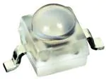
VEMD2503X01
• Package type: surface mount
VEMD2523X01
• Package form: GW, RGW
• Dimensions (L x W x H in mm): 2.3 x 2.3 x 2.55
• AEC-Q101 qualified
• High radiant sensitivity
• Suitable for visible and neat infrared radiation
• Fast response times
• Angle of half sensitivity: = ± 35°
• Package matched with IR emitter series
VSMB2943X01
DESCRIPTION
• Floor life: 4 weeks, MSL 2a, acc. J-STD-020
VEMD2503X01 and VEMD2523X01 are high speed and high
sensitive PIN photodiodes in a miniature surface mount
package (SMD) with dome lens. The clear epoxy allows light
detection of a wide wavelength range from 350 nm to
1120 nm. The photo sensitive area of the chip is 0.23 mm2.
• Lead (Pb)-free reflow soldering
• Material categorization: For definitions of compliance
please see www.vishay.com/doc?99912
APPLICATIONS
• High speed photo detector
• Light curtain
• Detector for optical switch
PRODUCT SUMMARY
COMPONENT
Ira (μA)
(deg)
0.1 (nm)
VEMD2503X01
10
± 35
350 to 1120
VEMD2523X01
10
± 35
350 to 1120
Note
• Test conditions see table “Basic Characteristics”
ORDERING INFORMATION
ORDERING CODE
PACKAGING
REMARKS
PACKAGE FORM
VEMD2503X01
Tape and reel
MOQ: 6000 pcs, 6000 pcs/reel
Reverse gullwing
VEMD2523X01
Tape and reel
MOQ: 6000 pcs, 6000 pcs/reel
Gullwing
Note
• MOQ: minimum order quantity
ABSOLUTE MAXIMUM RATINGS (Tamb = 25 °C, unless otherwise specified)
PARAMETER
TEST CONDITION
Reverse voltage
Power dissipation
Tamb 25 °C
Junction temperature
Operating temperature range
Storage temperature range
Soldering temperature
Thermal resistance junction/ambient
Rev. 1.0, 05-Apr-13
SYMBOL
VALUE
VR
60
UNIT
V
PV
215
mW
Tj
100
°C
Tamb
- 40 to + 100
°C
Tstg
- 40 to + 100
°C
Acc. reflow solder profile fig. 7
Tsd
260
°C
Acc. J-STD-051
RthJA
250
K/W
Document Number: 84163
1
For technical questions, contact: detectortechsupport@vishay.com
THIS DOCUMENT IS SUBJECT TO CHANGE WITHOUT NOTICE. THE PRODUCTS DESCRIBED HEREIN AND THIS DOCUMENT
ARE SUBJECT TO SPECIFIC DISCLAIMERS, SET FORTH AT www.vishay.com/doc?91000
�VEMD2503X01, VEMD2523X01
www.vishay.com
Vishay Semiconductors
BASIC CHARACTERISTICS (Tamb = 25 °C, unless otherwise specified)
PARAMETER
TEST CONDITION
SYMBOL
IF = 50 mA
VF
IR = 100 μA, E = 0
V(BR)
VR = 10 V, E = 0
Iro
Forward voltage
Breakdown voltage
Reverse dark current
Diode capacitance
Open circuit voltage
MIN.
TYP.
MAX.
UNIT
1
V
32
V
1
10
nA
VR = 0 V, f = 1 MHz, E = 0
CD
4
VR = 5 V, f = 1 MHz, E = 0
CD
1.3
pF
Ee = 1 mW/cm2, = 950 nm
Vo
350
mV
mV/K
pF
Temperature coefficient of Vo
Ee = 1 mW/cm2, = 950 nm
TKVo
- 2.6
Short circuit current
Ee = 1 mW/cm2, = 950 nm
Ik
10
μA
Temperature coefficient of Ik
Ee = 1 mW/cm2, = 950 nm
TKIk
0.1
%/K
Ee = 1 mW/cm2, = 950 nm, VR = 5 V
Ira
Reverse light current
7
Angle of half sensitivity
10
14
μA
± 35
deg
Wavelength of peak sensitivity
p
900
nm
Range of spectral bandwidth
0.1
350 to 1120
nm
Rise time
VR = 10 V, RL = 1 k, = 820 nm
tr
100
ns
Fall time
VR = 10 V, RL = 1 k, = 820 nm
tf
100
ns
BASIC CHARACTERISTICS (Tamb = 25 °C, unless otherwise specified)
100
Ira - Reverse Light Current (µA)
Iro - Reverse Dark Current (nA)
1000
100
10
VR = 10 V
1
20
94 8427
40
60
1
0.1
1
10
Ee - Irradiance (mW/cm2)
Tamb - Ambient Temperature (°C)
Fig. 1 - Reverse Dark Current vs. Ambient Temperature
Fig. 3 - Reverse Light Current vs. Irradiance
8
1.4
CD - Diode Capacitance (pF)
Ira, rel - Relative Reverse Light Current
10
0.1
0.01
100
80
VR = 5 V
VR = 5 V
λ = 950 nm
1.2
1.0
0.8
6
E=0
f = 1 MHz
4
2
0
0.6
0
94 8416
20
40
60
80
100
Tamb - Ambient Temperature (°C)
Fig. 2 - Relative Reverse Light Current vs. Ambient Temperature
Rev. 1.0, 05-Apr-13
0.1
94 8430
1
10
100
VR- Reverse Voltage (V)
Fig. 4 - Diode Capacitance vs. Reverse Voltage
Document Number: 84163
2
For technical questions, contact: detectortechsupport@vishay.com
THIS DOCUMENT IS SUBJECT TO CHANGE WITHOUT NOTICE. THE PRODUCTS DESCRIBED HEREIN AND THIS DOCUMENT
ARE SUBJECT TO SPECIFIC DISCLAIMERS, SET FORTH AT www.vishay.com/doc?91000
�VEMD2503X01, VEMD2523X01
www.vishay.com
Vishay Semiconductors
0°
10°
20°
30°
1.0
0.8
0.6
0.4
0.2
40°
1.0
0.9
50°
0.8
60°
70°
ϕ - Angular Displacement
Srel - Relative Radiant Sensitivity
S (λ)rel - Relative Spectral Sensitivity
1.2
80°
0
400
500
600
700
800
900
1000 1100
Fig. 5 - Relative Spectral Sensitivity vs. Wavelength
REFLOW SOLDER PROFILE
0.4
0.2
0
max. 260 °C
245 °C
255 °C
240 °C
217 °C
250
max. 30 s
150
max. 100 s
100
max. ramp up 3 °C/s max. ramp down 6 °C/s
50
0
0
19841
50
100
150
200
250
Devices are packed in moisture barrier bags (MBB) to
prevent the products from moisture absorption during
transportation and storage. Each bag contains a desiccant.
FLOOR LIFE
Floor life (time between soldering and removing from MBB)
must not exceed the time indicated on MBB label:
Floor life: 4 weeks
Conditions: Tamb < 30 °C, RH < 60 %
Moisture sensitivity level 2a, acc. to J-STD-020.
200
max. 120 s
Fig. 6 - Relative Radiant Intensity vs. Angular Displacement
DRYPACK
300
Temperature (°C)
0.7 0.6
λ - Wavelength (nm)
21553
300
Time (s)
DRYING
In case of moisture absorption devices should be baked
before soldering. Conditions see J-STD-020 or label.
Devices taped on reel dry using recommended conditions
192 h at 40 °C (+ 5 °C), RH < 5 %.
Fig. 7 - Lead (Pb)-free Reflow Solder Profile acc. J-STD-020D
Rev. 1.0, 05-Apr-13
Document Number: 84163
3
For technical questions, contact: detectortechsupport@vishay.com
THIS DOCUMENT IS SUBJECT TO CHANGE WITHOUT NOTICE. THE PRODUCTS DESCRIBED HEREIN AND THIS DOCUMENT
ARE SUBJECT TO SPECIFIC DISCLAIMERS, SET FORTH AT www.vishay.com/doc?91000
�VEMD2503X01, VEMD2523X01
www.vishay.com
Vishay Semiconductors
PACKAGE DIMENSIONS in millimeters: VEMD2503
Rev. 1.0, 05-Apr-13
Document Number: 84163
4
For technical questions, contact: detectortechsupport@vishay.com
THIS DOCUMENT IS SUBJECT TO CHANGE WITHOUT NOTICE. THE PRODUCTS DESCRIBED HEREIN AND THIS DOCUMENT
ARE SUBJECT TO SPECIFIC DISCLAIMERS, SET FORTH AT www.vishay.com/doc?91000
�VEMD2503X01, VEMD2523X01
www.vishay.com
Vishay Semiconductors
PACKAGE DIMENSIONS in millimeters: VEMD2523
Rev. 1.0, 05-Apr-13
Document Number: 84163
5
For technical questions, contact: detectortechsupport@vishay.com
THIS DOCUMENT IS SUBJECT TO CHANGE WITHOUT NOTICE. THE PRODUCTS DESCRIBED HEREIN AND THIS DOCUMENT
ARE SUBJECT TO SPECIFIC DISCLAIMERS, SET FORTH AT www.vishay.com/doc?91000
�VEMD2503X01, VEMD2523X01
www.vishay.com
Vishay Semiconductors
TAPING AND REEL DIMENSIONS in millimeters: VEMD2503
Rev. 1.0, 05-Apr-13
Document Number: 84163
6
For technical questions, contact: detectortechsupport@vishay.com
THIS DOCUMENT IS SUBJECT TO CHANGE WITHOUT NOTICE. THE PRODUCTS DESCRIBED HEREIN AND THIS DOCUMENT
ARE SUBJECT TO SPECIFIC DISCLAIMERS, SET FORTH AT www.vishay.com/doc?91000
�VEMD2503X01, VEMD2523X01
www.vishay.com
Vishay Semiconductors
TAPING AND REEL DIMENSIONS in millimeters: VEMD2523
Rev. 1.0, 05-Apr-13
Document Number: 84163
7
For technical questions, contact: detectortechsupport@vishay.com
THIS DOCUMENT IS SUBJECT TO CHANGE WITHOUT NOTICE. THE PRODUCTS DESCRIBED HEREIN AND THIS DOCUMENT
ARE SUBJECT TO SPECIFIC DISCLAIMERS, SET FORTH AT www.vishay.com/doc?91000
�Legal Disclaimer Notice
www.vishay.com
Vishay
Disclaimer
ALL PRODUCT, PRODUCT SPECIFICATIONS AND DATA ARE SUBJECT TO CHANGE WITHOUT NOTICE TO IMPROVE
RELIABILITY, FUNCTION OR DESIGN OR OTHERWISE.
Vishay Intertechnology, Inc., its affiliates, agents, and employees, and all persons acting on its or their behalf (collectively,
“Vishay”), disclaim any and all liability for any errors, inaccuracies or incompleteness contained in any datasheet or in any other
disclosure relating to any product.
Vishay makes no warranty, representation or guarantee regarding the suitability of the products for any particular purpose or
the continuing production of any product. To the maximum extent permitted by applicable law, Vishay disclaims (i) any and all
liability arising out of the application or use of any product, (ii) any and all liability, including without limitation special,
consequential or incidental damages, and (iii) any and all implied warranties, including warranties of fitness for particular
purpose, non-infringement and merchantability.
Statements regarding the suitability of products for certain types of applications are based on Vishay's knowledge of typical
requirements that are often placed on Vishay products in generic applications. Such statements are not binding statements
about the suitability of products for a particular application. It is the customer's responsibility to validate that a particular product
with the properties described in the product specification is suitable for use in a particular application. Parameters provided in
datasheets and / or specifications may vary in different applications and performance may vary over time. All operating
parameters, including typical parameters, must be validated for each customer application by the customer's technical experts.
Product specifications do not expand or otherwise modify Vishay's terms and conditions of purchase, including but not limited
to the warranty expressed therein.
Hyperlinks included in this datasheet may direct users to third-party websites. These links are provided as a convenience and
for informational purposes only. Inclusion of these hyperlinks does not constitute an endorsement or an approval by Vishay of
any of the products, services or opinions of the corporation, organization or individual associated with the third-party website.
Vishay disclaims any and all liability and bears no responsibility for the accuracy, legality or content of the third-party website
or for that of subsequent links.
Except as expressly indicated in writing, Vishay products are not designed for use in medical, life-saving, or life-sustaining
applications or for any other application in which the failure of the Vishay product could result in personal injury or death.
Customers using or selling Vishay products not expressly indicated for use in such applications do so at their own risk. Please
contact authorized Vishay personnel to obtain written terms and conditions regarding products designed for such applications.
No license, express or implied, by estoppel or otherwise, to any intellectual property rights is granted by this document or by
any conduct of Vishay. Product names and markings noted herein may be trademarks of their respective owners.
© 2022 VISHAY INTERTECHNOLOGY, INC. ALL RIGHTS RESERVED
Revision: 01-Jan-2022
1
Document Number: 91000
�


 工商网监
湘ICP备2023018690号
工商网监
湘ICP备2023018690号
