TC62D748CFNAG
TOSHIBA CDMOS Integrated Circuit Silicon Monolithic
TC62D748CFNAG
16-Output Constant Current LED Driver
The TC62D748CFNAG is a constant-current driver for LED
and LED display lighting applications.
The output current from each of the 16 outputs is
programmable via a single external resistor.
The TC62D748CFNAG contains a 16-channel shift register, a
16-channel latch, a 16-channel AND gate and a 16-channel
constant-current output.
Fabricated with a CMOS process, the TC62D748CFNAG allows
high-speed data transfer.
It operates with a 3.3- or 5-V power supply.
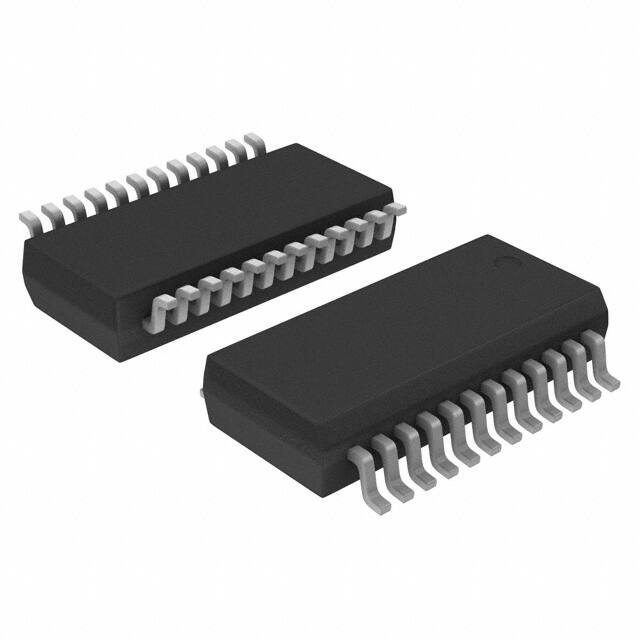
P-SSOP24-0409-0.64-001
Weight: 0.14 g (Typ.)
Features
•
Supply voltages
•
16-output built-in
: VDD = 3.3 V to 5.0 V
•
Output current setup range
•
Constant current output accuracy (@ REXT = 1.2 kΩ, VOUT = 1.0 V, VDD = 3.3 V, 5.0 V)
: IOUT = 1.5 to 90 mA
: S rank;between outputs ± 1.5 % (max)
: S rank;between devices: ± 1.5 % (max)
: N rank;between outputs ± 2.5 % (max)
: N rank;between devices: ± 2.5 % (max)
•
Output voltage
: VOUT = 17 V (max)
•
High-speed output switching
: twOE(L) = 25 ns (min), tor = 30ns (typ.), tof = 10ns (typ.)
•
I/O interface
: CMOS interfaces (Schmitt trigger input)
•
Data transfer frequency
: fSCK = 25 MHz (max)
•
Operation temperature range
: Topr = −40 to 85 °C
•
Power-on-reset function built-in. (When the power supply is turned on, internal data is reset)
•
Package
There is TC62D749 as an output switching high-speed version of this product.
: P-SSOP24-0409-0.64-001
For detailed part naming conventions, contact your local Toshiba sales representative or distributor.
1
2011-12-14
�TC62D748CFNAG
Block Diagram
OUT0
OUT1
OUT15
VDD
OUT0
OUT1
OUT15
B.G
Constant current outputs
POR
GND
VDD
REXT
OE
SLAT
SIN
G
D0
Q15
Q0 Q1
16-bit D-latch
D0 D1
D15
R
Q15
Q0 Q1
16-bit shift register
D15
R
SOUT
SCK
2
2011-12-14
�TC62D748CFNAG
Pin Assignment (top view)
GND
VDD
SIN
REXT
SCK
SOUT
SLAT
OE
OUT0
OUT15
OUT1
OUT14
OUT2
OUT13
OUT3
OUT12
OUT4
OUT11
OUT5
OUT10
OUT6
OUT9
OUT7
OUT8
Short circuiting an output pin to a power supply pin (Power-supply voltage VDD and LED anode power supply),
or short-circuiting the REXT pin to the GND pin will likely exceed the rating, which in turn may result in
smoldering and/or permanent damage. Please keep this in mind when determining the wiring layout for the power
supply and GND pins.
Pin Functions
Pin No
Pin Name
I/O
Function
1
GND
⎯
2
SIN
I
3
SCK
I
Serial data transfer clock input terminal
4
SLAT
I
Latch signal input pin.
5
OUT0
O
Constant-current output terminal
6
OUT1
O
Constant-current output terminal
7
OUT2
O
Constant-current output terminal
8
OUT3
O
Constant-current output terminal
9
OUT4
O
Constant-current output terminal
10
OUT5
O
Constant-current output terminal
11
OUT6
O
Constant-current output terminal
12
OUT7
O
Constant-current output terminal
13
OUT8
O
Constant-current output terminal
14
OUT9
O
Constant-current output terminal
15
OUT10
O
Constant-current output terminal
GND terminal
Serial data input terminal
16
OUT11
O
Constant-current output terminal
17
OUT12
O
Constant-current output terminal
18
OUT13
O
Constant-current output terminal
19
OUT14
O
Constant-current output terminal
20
OUT15
O
21
OE
I
22
SOUT
O
23
REXT
⎯
24
VDD
⎯
Constant-current output terminal
An output current enable signal input terminal
In "H" level input, outputs are turned off compulsorily.
In "L" level input, outputs are ON/OFF controlled according to serial data.
Serial data output terminal.
An external resistance for an output current setup is connected between
this terminal and ground.
Power supply terminal
3
2011-12-14
�TC62D748CFNAG
I/O Equivalent Circuits
2. OE
1. SCK, SIN
VDD
VDD
(SCK)
(SIN)
OE
GND
GND
3. SLAT
4. SOUT
VDD
VDD
SOUT
SLAT
GND
GND
5. OUT0 to OUT15
OUT0 to OUT15
GND
4
2011-12-14
�TC62D748CFNAG
Truth Table
SLAT
OE
SIN
OUT0 … OUT7 … OUT15 (Note1)
SOUT
H
L
Dn
Dn … Dn − 7 … Dn − 15
Dn − 15
L
L
Dn + 1
No Change
Dn − 14
H
L
Dn + 2
Dn + 2 … Dn − 5 … Dn − 13
Dn − 13
− (Note2)
L
Dn + 3
Dn + 2 … Dn − 5 … Dn − 13
Dn − 13
− (Note2)
H
Dn + 3
OFF
Dn − 13
SCK
Note1: When OUT0 to OUT15 output pins are set to "H" the respective output will be ON and when set to
"L" the respective output will be OFF.
Note2: “-“ is irrelevant to the truth table.
Timing Diagram
n=0
1
2
3
4
5
6
7
8
9
10 11 12 13 14 15
H
SCK
L
H
SIN
L
H
SLAT
L
H
OE
L
ON
OUT0
OFF
ON
OUT1
OFF
ON
OUT2
OFF
ON
OUT15
OFF
H
SOUT
L
・The latch circuit is a leveled-latch circuit. Please exercise precaution as it is not triggered-latch circuit.
・Keep the SLAT pin is set to “L” to enable the latch circuit to hold data. In addition, when the SLAT
pin is set to “H” the latch circuit does not hold data. The data will instead pass onto output.
When the OE pin is set to “L” the OUT0 to OUT15 output pins will go ON and OFF in response to
the data. In addition, when the OE pin is set to “H” all the output pins will be forced OFF regardless of
the data.
・This product can use 3.3V and 5.0V power supply, but power supply and input (SCK/SIN/ SLAT / OE )
must use same voltage.
5
2011-12-14
�TC62D748CFNAG
Absolute Maximum Ratings (Ta = 25°C)
Characteristics
Symbol
Rating (Note1)
Unit
S u p p l y
v o l t a g e
VDD
−0.3 to 6.0
V
O u t p u t
c u r r e n t
IOUT
95
mA
VIN
−0.3 to VDD + 0.3 (Note2)
V
VOUT
−0.3 to 17
V
L o g i c
i n p u t
v o l t a g e
O u t p u t
v o l t a g e
Operating
temperature
Topr
−40 to 85
°C
t e m p e r a t u r e
Tstg
−55 to 150
°C
Rth(j-a)
80.07
°C/W
PD
1.56 (Note3)
W
St o r a g e
T h e r m a l
P o w e r
r e s i s t a n c e
d i s s i p a t i o n
Note1: Voltage is ground referenced.
Note2: Do not exceed 6.0V.
Note3: The power dissipation decreases the reciprocal of the saturated thermal resistance (1/ Rth(j-a)) for each
degree (1°C) that the ambient temperature is exceeded (Ta = 25°C).
Operating Conditions
DC Items (Unless otherwise specified, VDD = 3.0 to 5.5 V, Ta = −40°C to 85°C)
Characteristics
Symbol
Test Conditions
Min
Typ.
Max
Unit
v o l t a g e
VDD
⎯
3.0
⎯
5.5
V
H i g h l e v e l l o g i c i n p u t v o l ta g e
VIH
Test terminal are SIN,SCK,
SLAT , OE
0.7 ×
VDD
⎯
VDD
V
Low level logic input voltage
VIL
Test terminal are SIN,SCK,
SLAT , OE
GND
⎯
0.3 ×
VDD
V
High level SOUT output current
IOH
⎯
⎯
⎯
−1
mA
Low level SOUT output current
IOL
⎯
⎯
⎯
1
mA
1.5
⎯
90
mA
S u p p l y
Constant
current
output
IOUT
Test terminal is
OUTn
AC Items (Unless otherwise specified, VDD = 3.0 to 5.5 V, Ta = −40°C to 85°C)
Characteristics
Symbol
Test
Circuits
Test Conditions
Min
Typ.
Max
Unit
S e r i a l d a ta t r a n s f e r f r e q u e n c y
fSCK
6
⎯
⎯
⎯
25
MHz
tHOLD1
6
⎯
5
⎯
⎯
ns
tHOLD2
6
⎯
5
⎯
⎯
ns
tSETUP1
6
⎯
5
⎯
⎯
ns
tSETUP2
6
⎯
5
⎯
⎯
ns
Maximum clock rise time
tr
6
(Note1)
⎯
⎯
500
ns
Maximum
tf
6
(Note1)
⎯
⎯
500
ns
Serial
Serial
data
data
Hold
time
Setup
time
clock
fall
time
Note1: If the device is connected in a cascade and the tr/tf of the clock waveform increases due to deceleration of the clock
waveform,it may not be possible to achieve the timing required for data transfer. Please keep these timing conditions in mind
when designing your application.
6
2011-12-14
�TC62D748CFNAG
Electrical Characteristics (Unless otherwise specified, VDD = 3.3V, Ta = 25°C)
Symbol
Test
Circuits
h
l e v e l
o u t p u t v ol ta g e
VOH
1
L
o
w
l
e
v
e
l
S O U T o u t p u t v ol ta g e
VOL
High level logic input current
Characteristics
Min
Typ.
Max
Unit
IOH = −1 mA
VDD −
0.4
⎯
⎯
V
1
IOL = +1 mA
⎯
⎯
0.4
V
IIH
2
VIN = VDD, OE , SIN, SCK
⎯
⎯
1
μA
Low level logic input current
IIL
3
VIN = GND, SLAT , SIN, SCK
⎯
⎯
−1
μA
Power
current
IDD
4
REXT = 1.2 kΩ, All output on
⎯
⎯
8.0
mA
c u r r e n t
IOUT
5
VDD = 3.3 V, VOUT = 1.0 V,
REXT = 1.2 kΩ, 1 output on
⎯
14.4
⎯
mA
Constant current error(Ch to Ch)
(
S
r
a
n
k
)
ΔIOUT(Ch)
5
VDD = 3.3 V, VOUT = 1.0 V,
REXT = 1.2 kΩ, 1 output on
⎯
⎯
±1.5
%
Constant current error(IC to IC)
(
S
r
a
n
k
)
ΔIOUT(IC)
5
VDD = 3.3 V, VOUT = 1.0 V,
REXT = 1.2 kΩ, 1 output on
⎯
⎯
±1.5
%
Constant current error(Ch to Ch)
(
N
r
a
n
k
)
ΔIOUT(Ch)
5
VDD = 3.3 V, VOUT = 1.0 V,
REXT = 1.2 kΩ, 1 output on
⎯
⎯
±2.5
%
Constant current error(IC to IC)
(
N
r
a
n
k
)
ΔIOUT(IC)
5
VDD = 3.3 V, VOUT = 1.0 V,
REXT = 1.2 kΩ, 1 output on
⎯
⎯
±2.5
%
IOK
5
VDD = 3.3 V, VOUT= 17 V,
REXT = 1.2 kΩ
⎯
⎯
0.5
μA
Constant current output power supply
v o l t a g e
r e g u l a t i o n
%VDD
5
VDD = 3.0 to 3.6 V, VOUT = 1.0 V,
REXT = 1.2 kΩ, 1 output on
⎯
±1
±5
%/V
Constant current output output voltage
r e g u l a t i o n
%VOUT
5
VDD = 3.3 V, VOUT = 1.0 to 3.0 V,
REXT = 1.2 kΩ, 1 output on
⎯
±0.1
±0.5
%/V
R (Up)
3
OE
400
500
600
kΩ
R (Down)
2
SLAT
400
500
600
kΩ
H i g
S O U T
supply
O u t p u t
Output
OFF
P u l l - u p
P u l l - d o w n
leak current
r e s i s t o r
r e s i s t o r
Test Conditions
7
2011-12-14
�TC62D748CFNAG
Electrical Characteristics (Unless otherwise specified, VDD = 5.0V, Ta = 25°C)
Symbol
Test
Circuits
h
l e v e l
o u t p u t v ol ta g e
VOH
1
L
o
w
l
e
v
e
l
S O U T o u t p u t v ol ta g e
VOL
High level logic input current
Characteristics
Min
Typ.
Max
Unit
IOH = −1 mA
VDD −
0.4
⎯
⎯
V
1
IOL = +1 mA
⎯
⎯
0.4
V
IIH
2
VIN = VDD, OE , SIN, SCK
⎯
⎯
1
μA
Low level logic input current
IIL
3
VIN = GND, SLAT , SIN, SCK
⎯
⎯
−1
μA
Power
IDD
4
REXT = 1.2 kΩ, All output on
⎯
⎯
8.0
mA
IOUT
5
VDD = 5.0 V, VOUT = 1.0 V,
REXT = 1.2 kΩ, 1 output on
⎯
14.4
⎯
mA
Constant current error(Ch to Ch)
(
S
r
a
n
k
)
ΔIOUT(Ch)
5
VDD = 3.3 V, VOUT = 1.0 V,
REXT = 1.2 kΩ, 1 output on
⎯
⎯
±1.5
%
Constant current error(IC to IC)
(
S
r
a
n
k
)
ΔIOUT(IC)
5
VDD = 3.3 V, VOUT = 1.0 V,
REXT = 1.2 kΩ, 1 output on
⎯
⎯
±1.5
%
Constant current error(Ch to Ch)
(
N
r
a
n
k
)
ΔIOUT(Ch)
5
VDD = 5.0 V, VOUT = 1.0 V,
REXT = 1.2 kΩ, 1 output on
⎯
⎯
±2.5
%
Constant current error(IC to IC)
(
N
r
a
n
k
)
ΔIOUT(IC)
5
VDD = 5.0 V, VOUT = 1.0 V,
REXT = 1.2 kΩ, 1 output on
⎯
⎯
±2.5
%
IOK
5
VDD = 5.0 V, VOUT = 17 V,
REXT = 1.2 kΩ
⎯
⎯
0.5
μA
Constant current output power supply
v o l t a g e
r e g u l a t i o n
%VDD
5
VDD = 4.5 to 5.5 V, VOUT = 1.0 V,
REXT = 1.2 kΩ, 1 output on
⎯
±1
±5
%/V
Constant current output output voltage
r e g u l a t i o n
%VOUT
5
VDD = 5.0 V, VOUT = 1.0 to 3.0 V,
REXT = 1.2 kΩ, 1 output on
⎯
±0.1
±0.5
%/V
R (Up)
3
OE
400
500
600
kΩ
R (Down)
2
SLAT
400
500
600
kΩ
H i g
S O U T
supply
O u t p u t
Output
OFF
P u l l - u p
P u l l - d o w n
current
c u r r e n t
leak current
r e s i s t o r
r e s i s t o r
Test Conditions
8
2011-12-14
�TC62D748CFNAG
Switching Characteristics (Unless otherwise specified, VDD = 3.3V, Ta = 25°C)
Symbol
Test
Circuits
SCK- OUT0
tpLH1
6
SLAT - OUT0
tpLH2
OE - OUT0
Characteristics
Propagation delay
t
i
m
e
Test Conditions
Min
Typ.
Max
Unit
SLAT = “H”, OE = “L”
⎯
50
65
ns
6
OE = “L”
⎯
50
65
ns
tpLH3
6
SLAT = “H”
⎯
50
65
ns
SCK-SOUT
tpLH
6
CL=10.5 pF
10
20
35
ns
SCK- OUT0
tpHL1
6
SLAT = “H”, OE = “L”
⎯
30
40
ns
SLAT - OUT0
tpHL2
6
OE = “L”
⎯
30
40
ns
OE - OUT0
tpHL3
6
SLAT = “H”
⎯
30
40
ns
SCK-SOUT
tpHL
6
CL=10.5 pF
10
20
35
ns
O u t p u t
r i s e
t i m e
tor
6
10 to 90% of voltage waveform
⎯
30
45
ns
O u t p u t
f a l l
t i m e
tof
6
90 to 10% of voltage waveform
⎯
10
20
ns
OE = “L”
25
⎯
⎯
w i d t h
twOE(L)
6
p u l s e
twOE(H)
6
OE = “H”
50
⎯
⎯
E n a b l e
ns
C l o c k
p u l s e
w i d t h
twSCK
6
SCK = “H” or “L”
20
⎯
⎯
ns
L a t c h
p u l s e
w i d t h
twSLAT
6
SLAT = “H”
20
⎯
⎯
ns
Switching Characteristics (Unless otherwise specified, VDD = 5.0V, Ta = 25°C)
Symbol
Test
Circuits
SCK- OUT0
tpLH1
6
SLAT - OUT0
tpLH2
OE - OUT0
tpLH3
SCK-SOUT
Characteristics
Propagation delay
t
i
m
e
Test Conditions
Min
Typ.
Max
Unit
SLAT = “H”, OE = “L”
⎯
50
65
ns
6
OE = “L”
⎯
50
65
ns
6
SLAT = “H”
⎯
50
65
ns
tpLH
6
CL=10.5 pF
10
20
35
ns
SCK- OUT0
tpHL1
6
SLAT = “H”, OE = “L”
⎯
30
40
ns
SLAT - OUT0
tpHL2
6
OE = “L”
⎯
30
40
ns
OE - OUT0
tpHL3
6
SLAT = “H”
⎯
30
40
ns
SCK-SOUT
tpHL
6
CL=10.5 pF
10
20
35
ns
O u t p u t
r i s e
t i m e
tor
6
10 to 90% of voltage waveform
⎯
30
45
ns
O u t p u t
f a l l
t i m e
tof
6
90 to 10% of voltage waveform
⎯
10
20
ns
OE = “L”
25
⎯
⎯
w i d t h
twOE(L)
6
p u l s e
twOE(H)
6
OE = “H”
50
⎯
⎯
E n a b l e
ns
C l o c k
p u l s e
w i d t h
twSCK
6
SCK = “H” or “L”
20
⎯
⎯
ns
L a t c h
p u l s e
w i d t h
twSLAT
6
SLAT = “H”
20
⎯
⎯
ns
9
2011-12-14
�TC62D748CFNAG
Test Circuits
Test Circuit1: High level SOUT output voltage / Low level SOUT output voltage
SCK
SIN
F.G
VDD
OUT0
SLAT
OUT7
OE
OUT15
GND
SOUT
CL = 10.5 pF
IO = -1mA to 1mA
REXT
V
VDD = 3.3 V, 5.0 V
VIH = VDD
VIL = 0 V
tr = tf = 10 ns
(10 to 90%)
Test Circuit2: High level logic input current / Pull-down resistor
VIN = VDD
A
A
A
SCK
SIN
VDD
OUT0
SLAT
A
OUT7
OE
OUT15
SOUT
VDD = 3.3 V, 5.0 V
GND
CL = 10.5 pF
REXT
Test Circuit3: Low level logic input current / Pull-up resistor
A
A
VDD
OUT0
SLAT
OUT7
OE
OUT15
REXT
GND
SOUT
10
VDD = 3.3 V, 5.0 V
A
SCK
SIN
CL = 10.5 pF
A
2011-12-14
�TC62D748CFNAG
Test Circuit4: Power supply current
F.G
SCK
SIN
VDD
OUT0
SLAT
OUT7
OE
OUT15
A
SOUT
VOUT = 1.0 V
VDD = 3.3 V, 5.0 V
GND
REXT = 1.2kΩ
REXT
CL = 10.5 pF
VIH = VDD
VIL = 0 V
tr = tf = 10 ns
(10 to 90%)
Test Circuit5: Constant current output / Output OFF leak current / Constant current error
Test Circuit5: Constant current output power supply voltage regulation
Constant current output output voltage regulation
VDD
OUT0
A
OUT7
A
OUT15
A
OE
GND
SOUT
CL = 10.5 pF
REXT
REXT = 1.2kΩ
VIH = VDD
VIL = 0 V
tr = tf = 10 ns
(10 to 90%)
VDD = 3.0~3.6 V, 4.5~5.5 V
SLAT
VOUT = 1.0~3.0 V, 17 V
F.G
SCK
SIN
Test Circuit6: Switching Characteristics
OUT0
SLAT
OUT7
OE
OUT15
GND
SOUT
CL = 10.5 pF
REXT
REXT = 1.2kΩ
VIH = VDD
VIL = 0 V
tr = tf = 10 ns
(10 to 90%)
11
RL = 300 Ω
CL
RL
CL
RL
CL = 10.5 pF
VDD = 3.3 V, 5.0 V
VDD
VLED = 5.32 V
F.G
SCK
SIN
2011-12-14
�TC62D748CFNAG
Timing Waveforms
1. SCK, SIN, SOUT
twSCK
SCK
50%
50%
tSETUP1
SIN
90%
50%
twSCK
50%
90%
10%
10%
tr
tf
50%
tHOLD1
SOUT
50%
tpLH/tpHL
2. SCK, SIN, SLAT , OE , OUT0
SCK
50%
50%
SIN
tHOLD2
SLAT
tSETUP2
50%
50%
twSLAT
twOE
50%
OE
OUT0
50%
50%
tpHL1/tpLH1
tpHL2/tpLH2
3. OE , OUT0 ~ OUT15
twOE
50%
50%
OE
tpLH3
tpHL3
90%
50%
50%
90%
OFF
OUT0 ~ OUT15
10%
10%
tof
ON
tor
12
2011-12-14
�TC62D748CFNAG
Power on reset (POR)
The TC62D748CFNAG provides a power-on reset to reset all internal data in order to prevent
malfunctions.
The POR circuitry works properly only when VDD rises from 0 V. To re-activate the POR circuitry, VDD
must be brought to less than 0.1 V. Internal data is guaranteed to be retained after VDD exceeds 3.0 V.
VDD waveform
VDD=3.0V
VDD voltage for guaranteed data
VDD=2.8 V
VDD voltage for end of reset
VDD=0.1 V
End of POR
VDD=0 V
POR working range
Beyond POR working range
13
POR working range
2011-12-14
�TC62D748CFNAG
Reference data
The above data is for reference only, not guaranteed. Careful evaluation is required prior to creating a
production design.
Output Current (IOUT) – Output current setting resistance (REXT)
IOUT - REXT
90
80
Theoretical formula
IOUT (A) = (1.04(V) ÷ REXT (Ω)) × 16.6
70
I OUT (mA)
60
50
40
30
20
10
VOUT=1.0V
Ta=25°C
0
0
1000
2000
3000
4000
5000
REXT (Ω)
14
2011-12-14
�TC62D748CFNAG
Reference data
The above data is for reference only, not guaranteed. Careful evaluation is required prior to creating a
production design.
Output current (IOUT) – Output voltage (VOUT)
IOUT - VOUT
VDD =3.3V,Ta=25℃,1chON
100
90
80
IOUT (mA)
70
60
50
40
30
20
10
0
0
0.5
1
1.5
VOUT (V)
2
2.5
3
2
2.5
3
IOUT - VOUT
VDD=5.0V,Ta=25℃,1chON
100
90
80
IOUT (mA)
70
60
50
40
30
20
10
0
0
0.5
1
1.5
VOUT (V)
15
2011-12-14
�TC62D748CFNAG
Application Circuit: General Composition for Static Lighting of LEDs
In the following diagram, it is recommended that the LED supply voltage (VLED) be equal to or greater than the sum of Vf (max) of all LEDs plus 1.0 V.
VLED
OUT14 OUT15
SOUT
OUT0 OUT1
SIN
C.U.
OE
OE
TC62D748CFNAG
SLAT
SLAT
SCK
SCK
REXT
GND
OUT14 OUT15
OUT0 OUT1
SIN
TC62D748CFNAG
REXT
16
SOUT
GND
2011-12-14
�TC62D748CFNAG
Application Circuit: General Composition for Dynamic Lighting of LEDs
In the following diagram, it is recommended that the LED supply voltage (VLED) be equal to or greater than the sum of Vf (max) of all LEDs plus 1.0 V.
VLED
OUT0
OUT1
OUT14
SIN
C.U.
OE
SLAT
OUT15
SOUT
OUT0
OE
TC62D748CFNAG
SLAT
SCK
OUT1
OUT14
SIN
OUT15
SOUT
TC62D748CFNAG
SCK
REXT
GND
REXT
17
GND
2011-12-14
�TC62D748CFNAG
Notes on design of ICs
1.Decoupling capacitors between power supply and GND
It is recommended to place decoupling capacitors between power supply and GND as close to the IC as
possible.
2.Output current setting resistors
When the output current setting resistors (REXT) are shared among multiple ICs, production design should
be evaluated carefully.
3.Board layout
Ground noise generated by output switching might cause the IC to malfunction if the ground line exhibits
inductance and resistance due to PC board traces and wire leads. Also, the inductance between the IC
output pins and the LED cathode pins might cause large surge voltage, damaging LEDs and the IC
outputs. To avoid this situation, PC board traces and wire leads should be carefully laid out.
4.Consult the latest technical information for mass production.
18
2011-12-14
�TC62D748CFNAG
Package Dimensions
CFNAG Type
P-SSOP24-0409-0.64-001
Unit: mm
Weight: 0.14 g (typ.)
19
2011-12-14
�TC62D748CFNAG
Notes on Contents
1. Block Diagrams
Some of the functional blocks, circuits, or constants in the block diagram may be omitted or simplified for
explanatory purposes.
2. Equivalent Circuits
The equivalent circuit diagrams may be simplified or some parts of them may be omitted for explanatory
purposes.
3. Timing Charts
Timing charts may be simplified for explanatory purposes.
4. Application Circuits
The application circuits shown in this document are provided for reference purposes only. Thorough
evaluation is required, especially at the mass production design stage.
Toshiba does not grant any license to any industrial property rights by providing these examples of
application circuits.
5. Test Circuits
Components in the test circuits are used only to obtain and confirm the device characteristics. These
components and circuits are not guaranteed to prevent malfunction or failure from occurring in the
application equipment.
20
2011-12-14
�TC62D748CFNAG
IC Usage Considerations
Notes on handling of ICs
[1] The absolute maximum ratings of a semiconductor device are a set of ratings that must not be exceeded,
even for a moment. Do not exceed any of these ratings.
Exceeding the rating(s) may cause the device breakdown, damage or deterioration, and may result injury
by explosion or combustion.
[2] Use an appropriate power supply fuse to ensure that a large current does not continuously flow in case of
over current and/or IC failure. The IC will fully break down when used under conditions that exceed its
absolute maximum ratings, when the wiring is routed improperly or when an abnormal pulse noise occurs
from the wiring or load, causing a large current to continuously flow and the breakdown can lead smoke or
ignition. To minimize the effects of the flow of a large current in case of breakdown, appropriate settings,
such as fuse capacity, fusing time and insertion circuit location, are required.
[3] If your design includes an inductive load such as a motor coil, incorporate a protection circuit into the
design to prevent device malfunction or breakdown caused by the current resulting from the inrush current
at power ON or the negative current resulting from the back electromotive force at power OFF. IC
breakdown may cause injury, smoke or ignition.
Use a stable power supply with ICs with built-in protection functions. If the power supply is unstable, the
protection function may not operate, causing IC breakdown. IC breakdown may cause injury, smoke or
ignition.
[4] Do not insert devices in the wrong orientation or incorrectly.
Make sure that the positive and negative terminals of power supplies are connected properly.
Otherwise, the current or power consumption may exceed the absolute maximum rating, and exceeding
the rating(s) may cause the device breakdown, damage or deterioration, and may result injury by
explosion or combustion.
In addition, do not use any device that is applied the current with inserting in the wrong orientation or
incorrectly even just one time.
[5] Carefully select external components (such as inputs and negative feedback capacitors) and load
components (such as speakers), for example, power amp and regulator.
If there is a large amount of leakage current such as input or negative feedback condenser, the IC output
DC voltage will increase. If this output voltage is connected to a speaker with low input withstand voltage,
overcurrent or IC failure can cause smoke or ignition. (The over current can cause smoke or ignition from
the IC itself.) In particular, please pay attention when using a Bridge Tied Load (BTL) connection type IC
that inputs output DC voltage to a speaker directly.
Points to remember on handling of ICs
(1) Heat Radiation Design
In using an IC with large current flow such as power amp, regulator or driver, please design the device so
that heat is appropriately radiated, not to exceed the specified junction temperature (TJ) at any time and
condition. These ICs generate heat even during normal use. An inadequate IC heat radiation design can
lead to decrease in IC life, deterioration of IC characteristics or IC breakdown. In addition, please design
the device taking into considerate the effect of IC heat radiation with peripheral components.
(2) Back-EMF
When a motor rotates in the reverse direction, stops or slows down abruptly, a current flow back to the
motor’s power supply due to the effect of back-EMF. If the current sink capability of the power supply is
small, the device’s motor power supply and output pins might be exposed to conditions beyond absolute
maximum ratings. To avoid this problem, take the effect of back-EMF into consideration in system design.
21
2011-12-14
�TC62D748CFNAG
About solderability, following conditions were confirmed
Solderability
(1)
·
·
·
·
Use of Sn-37Pb solder Bath
solder bath temperature: 230°C
dipping time: 5 seconds
the number of times: once
use of R-type flux
(2)
·
·
·
·
Use of Sn-3.0Ag-0.5Cu solder Bath
solder bath temperature: 245°C
dipping time: 5 seconds
the number of times: once
use of R-type flux
22
2011-12-14
�TC62D748CFNAG
RESTRICTIONS ON PRODUCT USE
• Toshiba Corporation, and its subsidiaries and affiliates (collectively “TOSHIBA”), reserve the right to make changes to the information
in this document, and related hardware, software and systems (collectively “Product”) without notice.
• This document and any information herein may not be reproduced without prior written permission from TOSHIBA. Even with
TOSHIBA’s written permission, reproduction is permissible only if reproduction is without alteration/omission.
• Though TOSHIBA works continually to improve Product’s quality and reliability, Product can malfunction or fail. Customers are
responsible for complying with safety standards and for providing adequate designs and safeguards for their hardware, software and
systems which minimize risk and avoid situations in which a malfunction or failure of Product could cause loss of human life, bodily
injury or damage to property, including data loss or corruption. Before customers use the Product, create designs including the Product,
or incorporate the Product into their own applications, customers must also refer to and comply with (a) the latest versions of all
relevant TOSHIBA information, including without limitation, this document, the specifications, the data sheets and application notes for
Product and the precautions and conditions set forth in the “TOSHIBA Semiconductor Reliability Handbook” and (b) the instructions for
the application with which the Product will be used with or for. Customers are solely responsible for all aspects of their own product
design or applications, including but not limited to (a) determining the appropriateness of the use of this Product in such design or
applications; (b) evaluating and determining the applicability of any information contained in this document, or in charts, diagrams,
programs, algorithms, sample application circuits, or any other referenced documents; and (c) validating all operating parameters for
such designs and applications. TOSHIBA ASSUMES NO LIABILITY FOR CUSTOMERS’ PRODUCT DESIGN OR APPLICATIONS.
• Product is intended for use in general electronics applications (e.g., computers, personal equipment, office equipment, measuring
equipment, industrial robots and home electronics appliances) or for specific applications as expressly stated in this document.
Product is neither intended nor warranted for use in equipment or systems that require extraordinarily high levels of quality and/or
reliability and/or a malfunction or failure of which may cause loss of human life, bodily injury, serious property damage or serious public
impact (“Unintended Use”). Unintended Use includes, without limitation, equipment used in nuclear facilities, equipment used in the
aerospace industry, medical equipment, equipment used for automobiles, trains, ships and other transportation, traffic signaling
equipment, equipment used to control combustions or explosions, safety devices, elevators and escalators, devices related to electric
power, and equipment used in finance-related fields. Do not use Product for Unintended Use unless specifically permitted in this
document.
• Do not disassemble, analyze, reverse-engineer, alter, modify, translate or copy Product, whether in whole or in part.
• Product shall not be used for or incorporated into any products or systems whose manufacture, use, or sale is prohibited under any
applicable laws or regulations.
• The information contained herein is presented only as guidance for Product use. No responsibility is assumed by TOSHIBA for any
infringement of patents or any other intellectual property rights of third parties that may result from the use of Product. No license to
any intellectual property right is granted by this document, whether express or implied, by estoppel or otherwise.
• ABSENT A WRITTEN SIGNED AGREEMENT, EXCEPT AS PROVIDED IN THE RELEVANT TERMS AND CONDITIONS OF SALE
FOR PRODUCT, AND TO THE MAXIMUM EXTENT ALLOWABLE BY LAW, TOSHIBA (1) ASSUMES NO LIABILITY
WHATSOEVER, INCLUDING WITHOUT LIMITATION, INDIRECT, CONSEQUENTIAL, SPECIAL, OR INCIDENTAL DAMAGES OR
LOSS, INCLUDING WITHOUT LIMITATION, LOSS OF PROFITS, LOSS OF OPPORTUNITIES, BUSINESS INTERRUPTION AND
LOSS OF DATA, AND (2) DISCLAIMS ANY AND ALL EXPRESS OR IMPLIED WARRANTIES AND CONDITIONS RELATED TO
SALE, USE OF PRODUCT, OR INFORMATION, INCLUDING WARRANTIES OR CONDITIONS OF MERCHANTABILITY, FITNESS
FOR A PARTICULAR PURPOSE, ACCURACY OF INFORMATION, OR NONINFRINGEMENT.
• Do not use or otherwise make available Product or related software or technology for any military purposes, including without limitation,
for the design, development, use, stockpiling or manufacturing of nuclear, chemical, or biological weapons or missile technology
products (mass destruction weapons). Product and related software and technology may be controlled under the Japanese Foreign
Exchange and Foreign Trade Law and the U.S. Export Administration Regulations. Export and re-export of Product or related software
or technology are strictly prohibited except in compliance with all applicable export laws and regulations.
• Please contact your TOSHIBA sales representative for details as to environmental matters such as the RoHS compatibility of Product.
Please use Product in compliance with all applicable laws and regulations that regulate the inclusion or use of controlled substances,
including without limitation, the EU RoHS Directive. TOSHIBA assumes no liability for damages or losses occurring as a result of
noncompliance with applicable laws and regulations.
23
2011-12-14
�


 工商网监
湘ICP备2023018690号
工商网监
湘ICP备2023018690号
