XT1861
Synchronous DC-DC Boost Converter
■ General Description
■ Features
XT1861 series is a high efficiency, low ripple , high
Maximum efficiency: 94%
frequency PFM control DC-DC boost converter.
Maximum operating frequency: 300KHz
XT1861 series requires only three external components,
Low Quiescent Current: 15μA
the device can change the low voltage input of battery
Output Voltage: 1.8V ~ 5.0V (step 0.1V)
step-up into output voltages for electronic devices.
Output Accuracy: ± 2.5%
Input voltage: 0.9V ~ 6.5V
low ripple and low noise
Small volume
■ Applications
1 to 3 batteries of electronic equipment
Electronic dictionaries, digital cameras
LED flashlights, LED Light,
Blood pressure monitors, MP3, remote control toys,
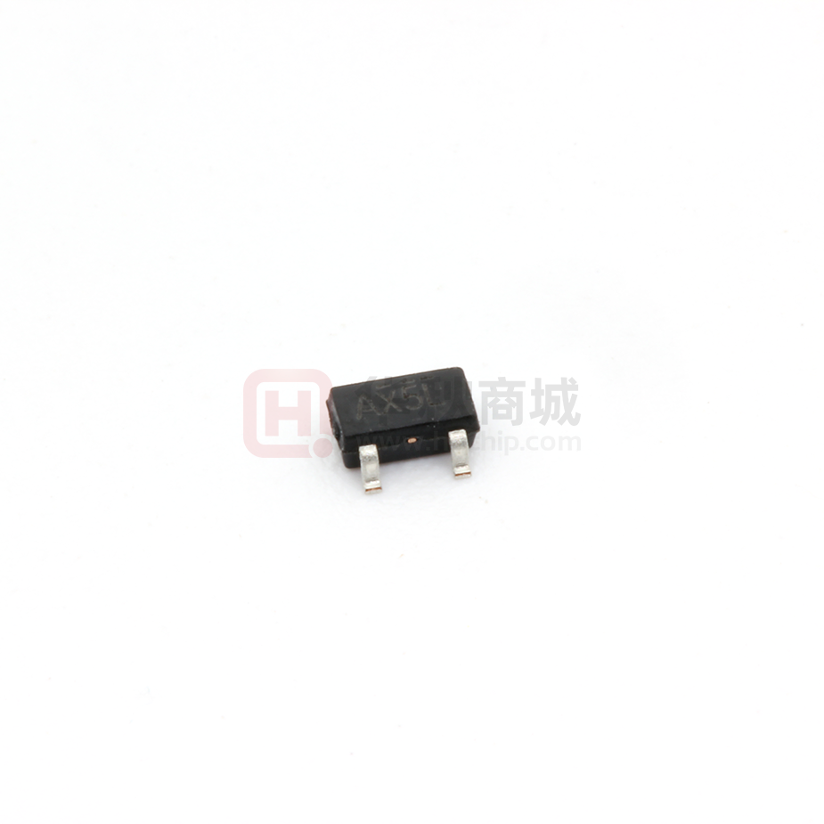
SOT-23-3L
Wireless headsets,wireless mouse, keyboard
SOT-23-3B
Medical devices, anti-lost alarm,
SOT-23-5L
Car alarm,charger,VCR,PDA and other handheld
SOT-89-3L
electronic devices
TO-92S
■ Package
TO-92
■ Typical Application Circuit
L
VIN
LX
VOUT
CIN
CE
VOUT
COUT
GND
GND
GND
Note: CIN=10µF, COUT=22 µF, L=10uH.
Rev.1.2 —Nov. 7. 2016
1
http://www.silinktek.com
�XT1861
■ Ordering Information
XT1861 B①②③④⑤
Designator
Symbol
①②
18-50
③
2
Precision:2%
M
Package Types: SOT-23-3L
V
Package Types: SOT-23-3B
S
Package Types: SOT-23-5L
P
Package Types: SOT89-3L
T
Package Types: TO-92S
L
Package Types: TO-92
R
Embossed Tape :Standard Feed
L
Embossed Tape :Reverse Feed
④
⑤
Description
Output Voltage: e.g. 33= 3.3V etc.
■ Pin Assignment
3
5
4
VOUT
LX
GND
GND VOUT LX
GND
LX
CE
VOUT
NC
GND
VOUT
LX
1
2
1
2
3
1
2
3
SOT-23-3L
(TOP VIEW)
SOT-23-5L
(TOP VIEW)
SOT-89-3L
(TOP VIEW)
1
2
3
TO-92
(FRONT VIEW)
GND VOUT LX
1
2
3
TO-92S
(FRONT VIEW)
■ Functional Pin Description
Pin Number
Pin Name
Function Description
3
LX
Switch pin
2
2
VOUT
Output pin
—
—
—
CE
Chip enable pin
4
1
1
1
GND
Ground
3
—
—
—
NC
NC
SOT-23-3L
SOT-23-5L
SOT-89-3L
TO-92S
TO-92
2
5
3
3
3
2
2
—
1
1
—
Rev.1.2 —Nov. 7. 2016
2
http://www.silinktek.com
�XT1861
■ Marking Rule
SOT-89-3L ,SOT-23-3L/B,SOT-23-5L,SOT89-3L,TO-92S,TO-92
. . . ..
.
. . . ..
.
① ② ③ ④
SOT-23-3L
(TOP VIEW)
. .. . .
.
① ② ③ ④
. . . ..
.
① ② ③ ④
① ② ③ ④
SOT-23-5L
(TOP VIEW)
SOT-89-3L
(TOP VIEW)
TO-92
(FRONT VIEW)
.....
.
①②③④
TO-92S
(FRONT VIEW)
① Represents the product name
Symbol
Product Name
A
XT1861B*****
② Represents the output voltage range
Output Voltage(V)
0.1~3.0
3.1~6.0
300KHz
T
X
180KHz
U
Y
100KHz
V
Z
③ Represents the output voltage
Symbol
Output Voltage(V)
Symbol
Output Voltage(V)
0
-
3.1
-
F
1.6
4.6
-
1
-
3.2
-
H
1.7
4.7
-
2
-
3.3
-
K
1.8
4.8
-
3
-
3.4
-
L
1.9
4.9
-
4
-
3.5
-
M
2
5.0
-
5
-
3.6
-
N
2.1
5.1
-
6
-
3.7
-
P
2.2
5.2
-
7
-
3.8
-
R
2.3
5.3
-
8
-
3.9
-
S
2.4
5.4
-
9
-
4
-
T
2.5
5.5
-
A
-
4.1
-
U
2.6
5.6
-
B
-
4.2
-
V
2.7
5.7
-
C
-
4.3
-
X
2.8
5.8
-
D
-
4.4
-
Y
2.9
5.9
-
E
1.5
4.5
-
Z
3
6.0
-
④ Represents the assembly lot No.
0-9,A-Z; 0-9,A-Z mirror writing,repeated(G,I,J,O,Q,W exception)
For example:A6TX, represents the output voltage of XT1861B552*R 5.5V。
Notes: "• "represents the batch number. "• "says" 1 ", dot not said "0"; For example: dot on the top of the "③", and the top
right of the "④", said "010010", used to track the product batch.
Rev.1.2 —Nov. 7. 2016
3
http://www.silinktek.com
�XT1861
■ Function Block Diagram
LX
VOUT
Current Limiting comparator
+
Error Amplifier
buffer
+
-
PFM
comtrol
1.24V
Band gap
OSC
300KHz
CE
GND
Chip
Enable
■ Absolute Maximum Ratings
Parameter
Input voltage
Current
Power dissipation
Symbol
Description
Typical
Unit
Vmax
Maximum voltage supply for VOUT and VLX pin
6.5
V
Maximum current in LX pin
1000
mA
SOT-23-3L maximum power dissipation
350
mW
SOT-23-3Bmaximum power dissipation
250
mW
SOT-23-5L maximum power dissipation
350
mW
SOT89-3L maximum power dissipation
500
mW
TO-92S maximum power dissipation
500
mW
ILXmax
PD
Tmin-max
Temperature
Tstorage
ESD
Rev.1.2 —Nov. 7. 2016
VESD
Operating Ambient Temperature
-40—85
Storage Temperature
-40—165
Body static pressure values
4
°C
2000
V
http://www.silinktek.com
�XT1861
■ Electrical Characteristics
Parameter
Symbol
Test condition
Min
Typ
Max
Units
Output voltage accuracy
△VOUT
-
-2.5
-
2.5
%
Maximum input voltage
VINMAX
-
0.9
-
6.5
V
Start voltage
VSTART
ILOAD=1mA,VIN:0→2V
-
-
0.8
V
Hold voltage
VHOLD
ILOAD=1mA,VIN:2→0V
0.6
-
-
V
Oscillation signal duty
cycle
DCOSC
-
-
-
78
%
η
-
-
90
94
%
Limit current
ILIMIT
-
600
800
1000
mA
Input current (No load)
LINO
VIN=1.8V,VOUT=3.0V
-
15
-
µA
Efficiency
■ Typical Performance Characteristics
1.
Active Current VS Input Voltage
2.
Output Current Limit VS Vin
Active Current VS Input Voltage
Current Limit VS Vin
40
1000
36
900
Output Current Limit (mA)
Active Current (uA)
32
TJ=25℃, IL=0mA, VOUT=3.3V
28
24
20
16
12
8
4
0
1.2
800
700
600
TJ=25℃,VOUT=3.3V
500
400
300
200
100
1.4
1.6
1.8
2.0
2.2
2.4
2.6
2.8
3.0
0
0.0
3.2
0.4
0.8
1.2
Input Voltage (V)
3.
Output Voltage VS Input Voltage
4.
100.0
5.4
97.5
4.8
95.0
2.8
3.2
TJ=25℃, VIN=2.3V, VOUT=3.3V
92.5
TJ=25℃, IL=0mA, VOUT=3.3V
Efficiency (%)
Output Voltage (V)
2.4
Efficiency VS Output Current
Output Voltage VS Input Voltage
3.6
3.0
2.4
90.0
87.5
85.0
1.8
82.5
1.2
80.0
0.6
77.5
0.0
0.0
2.0
Efficiency VS Output Current
6.0
4.2
1.6
Input Voltage (V)
75.0
0.4
0.8
1.2
1.6
2.0
2.4
2.8
3.2
0
Input Voltage (V)
Rev.1.2 —Nov. 7. 2016
30
60
90
120
150
180
210
240
270
300
Output Current (mA)
5
http://www.silinktek.com
�XT1861
5.
Efficiency VS Output Current
6.
Quiescent Current VS Temperature
Efficiency VS Output Current
Quiescent Current VS Temperature
100.0
40
97.5
36
TJ=25℃, VOUT=3.3V, IL=50mA
Quiescent Current (uA)
95.0
Efficiency (%)
92.5
90.0
87.5
85.0
82.5
80.0
77.5
75.0
1.4
32
VOUT=6.0V
28
24
20
16
12
8
4
1.6
1.8
2.0
2.2
2.4
2.6
2.8
3.0
0
-40
3.2
-20
0
7.
20
40
60
80
100
120
100
120
Temperature (℃)
Input Voltage (V)
Start Voltage VS Temperature
8.
Output Current Limit VS Temperature
Start Voltage VS Temperature
Output Current Limit VS Temperature
1.5
300
290
Output Current Limit (mA)
1.4
Start Voltage (V)
1.3
IL=0mA
1.2
1.1
1.0
280
VIN=2.3V
270
260
250
240
230
220
0.9
210
0.8
-40
-20
0
20
40
60
80
100
200
-40
120
-20
0
Temperature (℃)
9.
Maximum oscillation frequency VS Temperature
Maximum oscillation frequency VS Temperature
60
80
Oscillation Signal Duty Cycle VS Temperature
100
Oscillation Signal Duty Cycle (%)
Maximum oscillation frequency (MHZ)
40
10. Oscillation Signal Duty Cycle VS Temperature
600
550
500
VOUT=2.3V, LX=300Ω to VOUT
450
400
350
300
250
200
-40
20
Temperature (℃)
-20
0
20
40
60
80
100
VOUT=2.3V, LX=300Ω to VOUT
80
70
60
50
-40
120
Temperature (℃)
Rev.1.2 —Nov. 7. 2016
90
-20
0
20
40
60
80
100
120
Temperature (℃)
6
http://www.silinktek.com
�XT1861
11. Output Voltage VS Temperature
12. Load Regulation VS Temperature
Output Voltage VS Temperature
Load Regulation VS Temperature
3.40
90
80
3.35
Load Regulation (mV)
Output Voltage (V)
70
3.30
VIN=2.3V,IL=50mA
3.25
3.20
VIN=2.3V, IL=1mA to 100mA
60
50
40
30
20
3.15
10
3.10
-40
-20
0
20
40
60
80
100
0
-40
120
13. CE high Voltage VS
-20
0
20
40
60
80
100
120
Temperature (℃)
Temperature (℃)
Temperature
CE high Voltage VS Temperature
1.6
VIN=2.3V
1.4
CE high Voltage (V)
1.2
1.0
0.8
0.6
0.4
0.2
0.0
-40
-20
0
20
40
60
80
100
120
Temperature (℃)
Rev.1.2 —Nov. 7. 2016
7
http://www.silinktek.com
�XT1861
■ Package Information
SOT-23-3L
θ
D
b
E
E1
L
0.2
e
c
Symbol
Dimensions In Millimeters
A
A2
A1
e1
Dimensions In Inches
Min
Max
Min
Max
A
1.050
1.250
0.041
0.049
A1
0.000
0.100
0.000
0.004
A2
1.050
1.150
0.041
0.045
b
0.300
0.500
0.012
0.020
c
0.100
0.200
0.004
0.008
D
2.820
3.020
0.111
0.119
E
1.500
1.700
0.059
0.067
E1
2.650
2.950
0.104
0.116
e
0.950(BSC)
0.037(BSC)
e1
1.800
2.000
0.071
0.079
L
0.300
0.600
0.012
0.024
θ
0°
8°
0°
8°
Rev.1.2 —Nov. 7. 2016
8
http://www.silinktek.com
�XT1861
SOT-23-3B
θ
D
b
L
E
E1
L1
0.2
e
c
Symbol
A
A2
A1
e1
Dimensions In Millimeters
Dimensions In Inches
Min
Max
Min
Max
A
1.050
1.250
0.041
0.049
A1
0.000
0.100
0.000
0.004
A2
1.050
1.150
0.041
0.045
b
0.300
0.500
0.012
0.020
c
0.100
0.200
0.004
0.008
D
2.820
3.020
0.111
0.119
E
1.500
1.700
0.059
0.067
E1
2.650
2.950
0.104
0.116
e
0.950(BSC)
0.037(BSC)
e1
1.800
2.000
0.071
0.079
L
0.300
0.600
0.012
0.024
θ
0°
8°
0°
8°
Rev.1.2 —Nov. 7. 2016
9
http://www.silinktek.com
�XT1861
SOT-23-5L
θ
D
0.2
E
E1
L
b
e
c
Symbol
A
A2
A1
e1
Dimensions In Millimeters
Dimensions In Inches
Min
Max
Min
Max
A
1.050
1.250
0.041
0.049
A1
0.000
0.100
0.000
0.004
A2
1.050
1.150
0.041
0.045
b
0.300
0.500
0.012
0.020
c
0.100
0.200
0.004
0.008
D
2.820
3.020
0.111
0.119
E
1.500
1.700
0.059
0.067
E1
2.650
2.950
0.104
0.116
e
0.950(BSC)
0.037(BSC)
e1
1.800
2.000
0.071
0.079
L
0.300
0.600
0.012
0.024
θ
0°
8°
0°
8°
Rev.1.2 —Nov. 7. 2016
10
http://www.silinktek.com
�XT1861
SOT-89-3L
D
A
E
E1
D1
b1
L
e
b
c
e1
Symbol
Dimensions In Millimeters
Dimensions In Inches
Min
Max
Min
Max
A
1.400
1.600
0.055
0.063
b
0.320
0.520
0.013
0.020
b1
0.400
0.580
0.016
0.023
c
0.350
0.400
0.014
0.017
D
4.400
4.600
0.173
0.181
D1
1.550REF.
0.061REF.
E
2.300
2.600
0.091
0.102
E1
3.940
4.250
0.155
0.167
e
1.500TYP
0.060TYP
e1
3.000TYP
0.118TYP
L
Rev.1.2 —Nov. 7. 2016
0.900
1.200
11
0.035
0.047
http://www.silinktek.com
�XT1861
TO-92
D
A1
E
D1
L
h
A
C
b
Φ
e
e1
Symbol
Dimensions In Millimeters
Dimensions In Inches
Min
Max
Min
Max
A
3.300
3.700
0.130
0.146
A1
1.100
1.400
0.043
0.055
b
0.380
0.550
0.015
0.022
c
0.360
0.510
0.014
0.020
D
4.400
4.700
0.173
0.185
D1
3.430
E
4.300
e
0.135
4.700
0.169
1.270TYP
0.185
0.050TYP
e1
2.440
2.640
0.096
0.104
L
14.100
14.500
0.555
0.571
Φ
h
Rev.1.2 —Nov. 7. 2016
1.600
0.000
0.380
12
0.063
0.000
0.015
http://www.silinktek.com
�XT1861
TO-92S
D
D1
E
θ
C
A1
A
b1
L
b
e
e1
Symbol
Dimensions In Millimeters
Dimensions In Inches
Min
Max
Min
Max
A
1.420
1.620
0.056
0.064
A1
0.660
0.860
0.026
0.034
b
0.350
0.480
0.014
0.019
b1
0.400
0.550
0.016
0.022
c
0.360
0.510
0.014
0.020
D
3.900
4.100
0.154
0.161
D1
2.280
2.680
0.090
0.106
E
3.050
3.250
0.120
0.128
e
1.270TYP
0.050TYP
e1
2.440
2.640
0.096
0.104
L
15.100
15.500
0.594
0.610
θ
Rev.1.2 —Nov. 7. 2016
45°TYP
45°TYP
13
http://www.silinktek.com
�
很抱歉,暂时无法提供与“XT1861B362MR-G”相匹配的价格&库存,您可以联系我们找货
免费人工找货- 国内价格
- 5+0.32300
- 20+0.29450
- 100+0.26600
- 500+0.23750
- 1000+0.22420
- 2000+0.21470


 工商网监
湘ICP备2023018690号
工商网监
湘ICP备2023018690号
