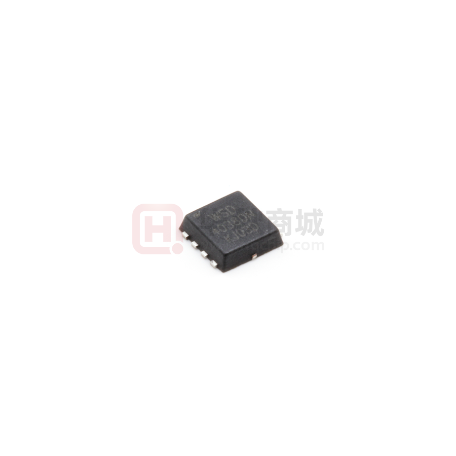
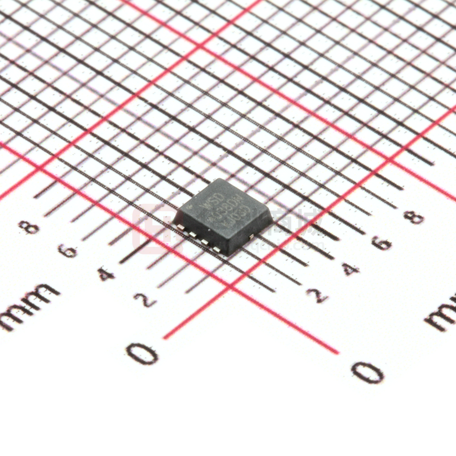
WSD4038DN
N-Ch MOSFET
General Description
Product Summery
The WSD4038DN is the highest
performance trench N-ch MOSFETs with
extreme high cell density , which provide
excellent RDSON and gate charge for
most of the synchronous buck converter
applications .
BVDSS
RDSON
ID
40V
13mΩ
38A
Applications
The WSD4038DN meet the RoHS and
Green Product requirement , 100%
EAS guaranteed with full function
reliability approved.
z High Frequency Point-of-Load Synchronous
Buck Converter for MB/NB/UMPC/VGA
z Networking DC-DC Power System
z Load Switch
Features
DFN3.3X3.3-EP Pin Configuration
z Advanced high cell density Trench technology
z Super Low Gate Charge
z Excellent CdV/dt effect decline
z 100% EAS Guaranteed
z Green Device Available
Absolute Maximum Ratings
Symbol
Parameter
Rating
Units
VDS
Drain-Source Voltage
40
V
VGS
Gate-Source Voltage
ID@TC=25℃
ID@TC=100℃
ID@TA=25℃
±20
V
1
38
A
1
20
A
1
15
A
1
10
A
36
A
26
mJ
Continuous Drain Current, VGS @ 10V
Continuous Drain Current, VGS @ 10V
Continuous Drain Current, VGS @ 10V
ID@TA=70℃
Continuous Drain Current, VGS @ 10V
IDM@TC=25℃
Pulsed Drain Current
EAS
IAS
PD@TA=25℃
2
Avalanche Energy ,Single Pulse (L=0.1mH)3
Avalanche Current ,Single pulse(L=0.1mH)3
36
A
4
2.1
W
4
Total Power Dissipation
PD@TA=70℃
Total Power Dissipation
1.78
W
TSTG
Storage Temperature Range
-55 to 150
℃
TJ
Operating Junction Temperature Range
-55 to 150
℃
Thermal Data
Symbol
Parameter
RθJA
Thermal Resistance Junction-Ambient
RθJC
1
www.winsok.tw
Thermal Resistance Junction-Case
Page 1
1
Typ.
Max.
Unit
---
60
℃/W
---
2.1
℃/W
Dec.2014
�WSD4038DN
N-Ch MOSFET
Electrical Characteristics (TJ=25 ℃, unless otherwise noted)
Symbol
BVDSS
RDS(ON)
RDS(ON)
VGS(th)
Parameter
Conditions
Drain-Source Breakdown Voltage
VGS=0V , ID=250uA
2
Static Drain-Source On-Resistance
2
Static Drain-Source On-Resistance
Gate Threshold Voltage
VGS=10V , ID=7A
VGS=4.5V , ID=5A
Min.
40
-----
Typ.
---
Max.
Unit
---
V
10.5
13
mΩ
12
16
mΩ
1.8
2.5
V
---
-6.
---
mV/℃
VDS=32V , VGS=0V , TJ=25℃
-----
-
2
VDS=32V , VGS=0V , TJ=55℃
---
-
10
VGS=±20V , VDS=0V
-----
-
±100
nA
VDS=5V , ID=20A
---
31
---
S
VDS=0V , VGS=0V , f=1MHz
---
1.1
1.8
Ω
---
20
28
---
3.9
7.5
---
3.0
5.1
---
12.6
16
---
10
12
---
23.6
32
Fall Time
---
6
9
Ciss
Input Capacitance
---
1125
---
Coss
Output Capacitance
---
132
---
Crss
Reverse Transfer Capacitance
---
70
---
Min.
Typ.
Max.
Unit
--
---
5
A
---
-
15
A
-----
-
1.1
V
△VGS(th)
VGS(th) Temperature Coefficient
IDSS
Drain-Source Leakage Current
IGSS
Gate-Source Leakage Current
gf
gfs
orward Transconductance
Rg
Gate Resistance
Qg
Total Gate Charge (10V)
Qgs
Qgd
Td(on)
Tr
Td(off)
Tf
VGS=VDS , ID =250uA
VDS=20V, VGS=10V, IDS=7A
Gate-Source Charge
Gate-Drain Charge
Turn-On Delay Time
VDD=20V, RL=20
3, IDS=1A, VGEN=10V,
RG=1Ω.
Rise Time
Turn-Off Delay Time
VDS=20V , VGS=0V , f=1MHz
1.5
uA
nC
ns
pF
Diode Characteristics
Symbol
IS
Parameter
Conditions
1,6
Continuous Source Current
2,6
ISM
Pulsed Source Current
VSD
Diode Forward Voltage2
VG=VD=0V , Force Current
VGS=0V , IS=20A , TJ=25℃
Note :
1.The data tested by surface mounted on a 1 inch2 FR-4 board with 2OZ copper,t
很抱歉,暂时无法提供与“WSD4038DN”相匹配的价格&库存,您可以联系我们找货
免费人工找货- 国内价格
- 1+1.34136
- 10+1.21716
- 30+1.13436
- 100+1.01016
- 500+0.95220
- 1000+0.91080


 工商网监
湘ICP备2023018690号
工商网监
湘ICP备2023018690号
