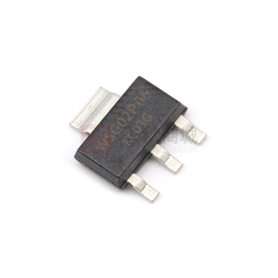
WSG02P06
P-Ch MOSFET
General Description
Product Summery
This P-Channel enhancement mode power
FETs are produced with high cell density, DMOS
trench technology, which is especially used to
minimize on-state resistance. This device is
particularly suited for low voltage application
such as portable equipment, power management
and other battery powered circuits, and low inline power loss are needed in a very small outline
surface mount package.
BVDSS
RDSON
ID
-60V
215mΩ
-2A
Applications
z High Frequency Point-of-Load Synchronous
Buck Converter.
z Networking DC-DC Power System
z Load Switch
Features
SOT-223 Pin Configuration
z Advanced high cell density Trench technology
z Super Low Gate Charge
z Excellent CdV/dt effect decline
z 100% EAS Guaranteed
z Green Device Available
Absolute Maximum Ratings
Symbol
Parameter
Rating
Units
VDS
Drain-Source Voltage
-60
V
VGS
Gate-Source Voltage
±20
V
ID@TA=25℃
Continuous Drain Current, VGS @ -10V
-2
A
ID@TA=70℃
Continuous Drain Current, VGS @ -10V
-1.6
A
IDM
Pulsed Drain Current
A
PD@TA=25℃
Total Power Dissipation
-10
2
W
TSTG
Storage Temperature Range
-55 to 150
℃
TJ
Operating Junction Temperature Range
-55 to 150
℃
Thermal Data
Symbol
Parameter
Typ.
Max.
Unit
RθJA
Thermal Resistance Junction-Ambient
---
62
℃/W
RθJC
Thermal Resistance Junction-Case
---
5.4
℃/W
www.winsok.tw
Page 1
Rev 1: Apr.2019
�WSG02P06
P-Ch MOSFET
Electrical Characteristics (TJ=25 ℃, unless otherwise noted)
Symbol
BVDSS
Parameter
Drain-Source Breakdown Voltage
△BVDSS/△TJ BVDSS Temperature Coefficient
RDS(ON)
Static Drain-Source On-Resistance
VGS(th)
Gate Threshold Voltage
△VGS(th)
VGS(th) Temperature Coefficient
Conditions
Min.
Typ.
Max.
Unit
-60
---
---
V
---
-0.03
---
V/℃
---
175
215
---
205
260
-1.2
-1.9
-3.0
V
---
4.56
---
mV/℃
VDS=-60V , VGS=0V , TJ=25℃
---
---
-1
VDS=-60V , VGS=0V , TJ=55℃
---
---
-5
VGS=±20V , VDS=0V
---
---
±100
nA
---
5
---
S
---
6.3
---
---
2.3
---
=
VGS=0V , ID -250uA
Reference to 25℃ , ID=-1mA
=
VGS=-10V , ID -2A
=
VGS=-4.5V , ID -2A
VGS=VDS , ID =-250uA
IDSS
Drain-Source Leakage Current
IGSS
Gate-Source Leakage Current
gfs
Forward Transconductance
Qg
Total Gate Charge
Qgs
Gate-Source Charge
Qgd
Gate-Drain Charge
---
1.8
---
Turn-On Delay Time
---
20
---
Td(on)
Tr
Td(off)
=
VDS=-15V , ID -2A
VDS=-48V , VGS=-4.5V , ID=-1A
Rise Time
VDD=-30V , VGS=-10V ,
---
.3
---
Turn-Off Delay Time
RGEN=3.3Ω,RL=30Ω.
---
5.2
---
Fall Time
---
3.8
---
Ciss
Input Capacitance
---
364
---
Coss
Output Capacitance
---
41
---
Crss
Reverse Transfer Capacitance
---
12
---
Tf
VDS=-15V , VGS=0V , f=1MHz
mΩ
uA
nC
ns
pF
Diode Characteristics
Symbol
IS
VSD
Parameter
Continuous Source Current
Diode Forward Voltage
Min.
Typ.
Max.
Unit
VG=VD=0V , Force Current
Conditions
---
---
-2
A
VGS=0V , IS=-1.2A , TJ=25℃
---
---
-1.2
V
A: The value of RθJA is measured with the device mounted on 1in² FR-4 board with 2oz. Copper, in a still air environment with TA =25°C. The value in any
given application depends on the user's specific board design.
B: The power dissipation PD is based on TJ(MAX)=150℃, u s i n g ≤10s junction-to-ambient thermal resistance.
C: Repetitive rating, pulse width limited by junction temperature TJ(MAX)=150℃. Ratings are based on low frequency and duty cycles to keep initial T J=25℃.
D: The RθJA is the sum of the thermal impedence from junction to lead RθJA and lead to ambient.
E: The static characteristics in Figures 1 to 6 are obtained using
很抱歉,暂时无法提供与“WSG02P06”相匹配的价格&库存,您可以联系我们找货
免费人工找货- 国内价格
- 1+0.77500
- 10+0.72500
- 50+0.65000
- 150+0.60000
- 300+0.56500
- 500+0.55000


 工商网监
湘ICP备2023018690号
工商网监
湘ICP备2023018690号
