Advanced Science And Novel Technology Company, Inc.
2790 Skypark Drive Suite 112, Torrance, CA 90505
Offices: 310-530-9400 / Fax: 310-530-9402
www.adsantec.com
ASNT8151-KMC
24.0-to-32.1GHz Programmable PLL with 3 integrated VCOs
Fully differential CML output full-rate clock interface
Selectable LVDS output clock divided-by-16 interface
3-state input control interface
Single positive or negative power supply
Power consumption: 0.53W at the maximum operational speed
Fabricated in SiGe for high performance, yield, and reliability
Custom CQFP 24-pin package
vee
LVDS input reference clock interface
vcc
crn
External RC loop filter
vcc
crp
Programmable clock multiplier (CMU) with three selectable frequency ranges of internal PLL
vcc
fltr
vcc
vcc
c16n
vc1
ASNT8151
vcc
vcc
c16p
vc0
vcc
vcc
Rev. 1.6.2
1
vcc
cn
vcc
cp
vcc
vee
vee
February 2020
�Advanced Science And Novel Technology Company, Inc.
2790 Skypark Drive Suite 112, Torrance, CA 90505
Offices: 310-530-9400 / Fax: 310-530-9402
www.adsantec.com
DESCRIPTION
fltr
crp
crn
vc0
vc1
LS
CIB
C
PLL
C16
CRL
HS
COB
cp
cn
LS
COB
c16p
c16n
Fig. 1. Functional Block Diagram
ASNT8151-KMC is a clock multiplication unit (CMU) with a triple-range phase-locked loop (PLL)
incorporating three high-speed voltage-controlled oscillators: VCO1 (lower frequency), VCO2 (medium
frequency), and VCO3 (higher frequency). The chip shown in Fig. 1 generates a high-speed clock signal
cp/cn with its phase and frequency locked to those of the incoming reference clock crp/crn. The
differential clock cp/cn with frequency f is delivered to the output by CML output buffer HS COB. The
reference clock crp/crn with frequency f/16 is accepted by LVDS input buffer LS CIB. The chip also
generates a divided-by-16 clock signal c16p/c16n with frequency f/16 that is delivered to the output by
LVDS output buffer LS COB. One of the VCOs is activated using two 3-state control signals vc0 and
vc1. The same control signals are used to activate or disable the output buffer LS COB.
When operating in closed-loop mode, the PLL requires an external loop filter connected to pin fltr. The
PLL also supports an open-loop mode of operation with its selected VCO controlled externally by a
voltage applied to the filter pin fltr.
The part’s high-speed output buffer supports the CML logic interface with on chip 50Ohm termination to
vcc and may be used differentially, AC/DC coupled, single-ended, or in any combination. The part’s lowspeed I/Os support the LVDS interface with internal 100Ohm termination between the direct and inverted
lines. The differential DC signaling mode is recommended for optimal performance.
LS CIB
The Low-Speed Clock Input Buffer (LS CIB) can process an external reference clock signal crp/crn with
a frequency equal to 1/16 of the selected VCO frequency. The clock inputs support the LVDS logic
interface with on chip 100Ohm termination between the direct and inverted lines. The proprietary LVDS
buffer exceeds the requirements of standards IEEE Std. 1596.3-1996 and ANSI/TIA/EIA-644-1995.
It is designed to accept a differential signal with a wide range of DC common mode voltages, or a singleended (SE) signal applied to one input pin with a DC threshold voltage applied to the other input pin. In
case of a SE AC-terminated input, the common mode voltage should satisfy the requirements presented in
ELECTRICAL CHARACTERISTICS. In case of a SE DC-terminated input, the DC common mode
voltage should match the average level of the applied reference clock signal.
Rev. 1.6.2
2
February 2020
�Advanced Science And Novel Technology Company, Inc.
2790 Skypark Drive Suite 112, Torrance, CA 90505
Offices: 310-530-9400 / Fax: 310-530-9402
www.adsantec.com
PLL
The PLL contains a phase frequency detector, a charge pump, an on-chip integrator with an additional offchip filter connected to pin fltr, and three selectable LC-tank VCOs with different central frequencies. The
recommended parameters of the external filter schematic components shown in Fig. 2 are for reference
only, and can be modified based on specific requirements.
a.
b.
Fig. 2. External Filter Schematic for Positive (a) and Negative (b) Power Supplies
The main function of the PLL is to synthesize a full-rate clock C by aligning the phase and frequency of
the divided clock C16 from the internal divider to the externally applied reference clock crp/crn. The
divided clock is delivered to outputs c16p/c16n through a CML output buffer LS COB. Selection of the
required VCO is defined by the CMOS control signals vc0 and vc1 as shown in Table 1. The same
signals are used to activate the LS COB block. Here “nc” means “not connected”.
Table 1. VCO and LS COB Control Modes
vc0
“0”
“0”
“0”
nc
nc
nc
”1”
”1”
”1”
vc1
Selected VCO
LS COB
“0” VCO1 (lower frequency)
On
nc VCO1 (lower frequency)
Off
”1”
VCO2 (medium frequency)
On
“0”
VCO3 (higher frequency) Off
nc VCO1 (lower frequency)
Off
”1”
VCO2 (medium frequency)
Off
“0”
VCO3 (higher frequency)
On
nc
VCO3 (higher frequency) Off
”1”
VCO2 (medium frequency)
On
The PLL can also operate in open-loop mode with an external control voltage applied to pin fltr. In this
case, the unused VCO is completely disabled in order to save power. The allowed control range is shown
in Table 2.
Table 2. VCO Control Voltage
fltr voltage, V
vcc
vcc-2.5
Rev. 1.6.2
Frequency of the active VCO
min
max
3
February 2020
�Advanced Science And Novel Technology Company, Inc.
2790 Skypark Drive Suite 112, Torrance, CA 90505
Offices: 310-530-9400 / Fax: 310-530-9402
www.adsantec.com
HS COB
The High Speed Clock Output Buffer (HS COB) receives a full-rate clock C from the PLL and converts it
into CML output signal cp/cn. The buffer provides an internal single-ended termination of 50Ohm to vcc
for each output line and also requires 50Ohm external termination resistors to be connected between vcc
and each output.
LS COB
The Low-Speed Clock Output Buffer (COB) receives the divided-by-16 clock signal from the PLL’s
divider and converts it into LVDS output signal c16p/c16n. The proprietary low-power LVDS output
buffer utilizes a special architecture that ensures operation at frequencies up to 2.5GHz with low power
consumption. The buffer satisfies all requirements of the IEEE Std. 1596.3-1996 and ANSI/TIA/EIA-6441995. For correct operation, it requires external differential 100Ohm DC termination at the receiver side.
The output pins should NEVER be CONNECTED to devices with 50Ohm termination to ground
WITHOUT DC BLOCKS!
The buffer can be enabled or disabled by the external 3-state control signals vc0 and vc1 as shown in
Table 1 above.
POWER SUPPLY CONFIGURATION
The part can operate with either negative supply (vcc = 0.0V = ground and vee = -2.8V or −3.3V), or
positive supply (vcc = +2.8V or +3.3V and vee = 0.0V = ground). In case of the positive supply, all CML
I/Os need AC termination when connected to any devices with 50Ohm termination to ground. Different
PCB layouts will be needed for each different power supply combination.
All the characteristics detailed below assume vee = 0.0V and vcc = +3.3V.
ABSOLUTE MAXIMUM RATINGS
Caution: Exceeding the absolute maximum ratings shown in Table 3 may cause damage to this product
and/or lead to reduced reliability. Functional performance is specified over the recommended operating
conditions for power supply and temperature only. AC and DC device characteristics at or beyond the
absolute maximum ratings are not assumed or implied. All min and max voltage limits are referenced to
ground (assumed vee).
Table 3. Absolute Maximum Ratings
Parameter
Supply Voltage (vcc)
Power Consumption
Input Voltage Swing (SE)
Case Temperature
Storage Temperature
Operational Humidity
Storage Humidity
Rev. 1.6.2
Min
-40
10
10
4
Max
3.6
580
1.0
+90
+100
98
98
Units
V
mW
V
ºC
ºC
%
%
February 2020
�Advanced Science And Novel Technology Company, Inc.
2790 Skypark Drive Suite 112, Torrance, CA 90505
Offices: 310-530-9400 / Fax: 310-530-9402
www.adsantec.com
TERMINAL FUNCTIONS
TERMINAL
Name
No. Type
cp
cn
3
5
crp
crn
c16p
c16n
17
15
23
21
vc0
vc1
fltr
Name
vcc
vee
Rev. 1.6.2
9
11
19
DESCRIPTION
High-Speed I/Os
Output CML differential clock outputs with internal SE 50Ohm termination
to vcc. Require external SE 50Ohm termination to vcc
Low-Speed I/Os
Input LVDS/CML clock inputs. See LS CIB for allowed application
schemes
Output LVDS clock outputs. See LS COB for a detailed description
Input
Input
Controls
3-state control signals
Pin for connecting the external loop filter. Can be also used for VCO
external control in open-loop mode
Supply and Termination Voltages
Description
Pin Number
Positive power supply (+2.8V or +3.3V)
2, 4, 6, 8, 10, 12, 14, 16, 18, 20, 22, 24
External ground (0V )
1, 7, 13
5
February 2020
�Advanced Science And Novel Technology Company, Inc.
2790 Skypark Drive Suite 112, Torrance, CA 90505
Offices: 310-530-9400 / Fax: 310-530-9402
www.adsantec.com
ELECTRICAL CHARACTERISTICS
PARAMETER
vee
vcc
Ivcc
Power consumption
Junction temperature
Frequency
Swing
CM Voltage Level
Frequency
Logic “1” level
Logic “0” level
Jitter
Duty Cycle
Phase Noise
Frequency
Interface
Logic “1” level
“nc” level
Logic “0” level
Low frequency of VCO1
High frequency of VCO1
Low frequency of VCO2
High frequency of VCO2
Low frequency of VCO3
High frequency of VCO3
External control voltage
range
MIN
TYP MAX
UNIT
COMMENTS
General Parameters
0.0
V
External ground
2.8 / 3.3
V
±5%
160
mA
450 / 530
mW
-25
50
125
°C
LS Input Reference Clock (crp/crn)
1.50
2.006
GHz
1/16 of the VCO frequency
200
800
mV
Differential, p-p
1.2
vcc-0.4
V
HS Output Clock (cp/cn)
24.0
32.1
GHz
Matches VCO frequency
V
vcc
vcc-0.55
V
200
fs
Peak-to-peak at 25.78GHz
50%
108
dBc/Hz
At 32GHz at 1.0MHz offset
LS Output Clock (c16p/c16n)
1.50
2.006
GHz
LVDS
Meets the IEEE Std.
3-State control inputs (vc0, vc1)
vcc-0.3
V
(vcc+vee)/2
Recommended to keep not
connected. The required level is
created internally.
vee+0.3
V
VCOs
24.0
GHz
Lower-frequency VCO
27.5
GHz
25.3
GHz
Medium-frequency VCO
27.7
GHz
27.5
GHz
Higher-frequency VCO
32.1
GHz
vcc-2.5
vcc
V
In open-loop mode
PACKAGE INFORMATION
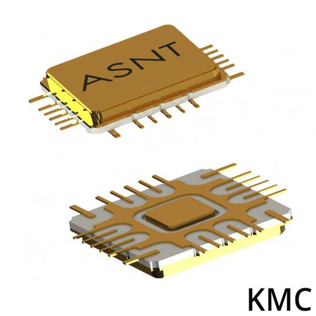
The chip die is housed in a custom 24-pin CQFP package shown in Fig. 3. The package provides a center
heat slug located on its back side to be used for heat dissipation. ADSANTEC recommends for this
section to be soldered to the vcc plain, which is ground for a negative supply, or power for a positive
supply.
Rev. 1.6.2
6
February 2020
�Advanced Science And Novel Technology Company, Inc.
2790 Skypark Drive Suite 112, Torrance, CA 90505
Offices: 310-530-9400 / Fax: 310-530-9402
www.adsantec.com
Fig. 3. CQFP 24-Pin Package Drawing (All Dimensions in mm)
The part’s identification label is ASNT8151-KMC. The first 8 characters of the name before the dash
identify the bare die including general circuit family, fabrication technology, specific circuit type, and part
version while the 3 characters after the dash represent the package’s manufacturer, type, and pin out
count.
This device complies with the Restriction of Hazardous Substances (RoHS) per 2011/65/EU for all ten
substances.
Rev. 1.6.2
7
February 2020
�Advanced Science And Novel Technology Company, Inc.
2790 Skypark Drive Suite 112, Torrance, CA 90505
Offices: 310-530-9400 / Fax: 310-530-9402
www.adsantec.com
REVISION HISTORY
Revision
1.6.2
1.5.2
1.5.1
Date
02-2020
07-2019
08-2015
1.4.1
1.3.1
04-2015
09-2014
1.2.1
05-2013
1.1.1
04-2013
1.0.1
03-2013
Rev. 1.6.2
Changes
Updated Package Information
Updated Letterhead
Updated External Filter Schematics
Updated electrical characteristics
Updated package information section
Updated clock output jitter value
Updated lower frequency of operation
Updated lower frequency in electrical characteristics table
Corrected title
Corrected filter schematics
Corrected power supply configurations
Corrected electrical characteristics
Corrected title
Corrected electrical characteristics
Initial release
8
February 2020
�


 工商网监
湘ICP备2023018690号
工商网监
湘ICP备2023018690号

