AOD409
P-Channel MOSFET Transistor
to
r
·FEATURES
·TO-252( DPAK ) packaging
·High speed switching
·Low gate input resistance
·Standard level gate drive
·Easy to use
·100% avalanche tested
·Minimum Lot-to-Lot variations for robust device
uc
performance and reliable operation
co
nd
·APPLICATIONS
·Power supply
·Switching applications
PARAMETER
VDSS
Drain-Source Voltage
VGSS
Gate-Source Voltage
VALUE
UNIT
-60
V
±20
V
Se
SYMBOL
mi
·ABSOLUTE MAXIMUM RATINGS(Ta=25℃)
Drain Current-Continuous@TC=25℃
TC=100℃
-26
-18
A
IDM
Drain Current-Single Pulsed
-60
A
PD
Total Dissipation
60
W
Tj
Operating Junction Temperature
175
℃
-55~175
℃
JS
MI
CR
O
ID
Tstg
Storage Temperature
·THERMAL CHARACTERISTICS
SYMBOL
PARAMETER
MAX
UNIT
Rth(ch-c)
Channel-to-case thermal resistance
2.5
℃/W
Rth(ch-a)
Channel-to-ambient thermal resistance
50
℃/W
www.jsmsemi.com
第1/2页
�AOD409
P-Channel MOSFET Transistor
ELECTRICAL CHARACTERISTICS
TC=25℃ unless otherwise specified
PARAMETER
CONDITIONS
MIN
BVDSS
Drain-Source Breakdown Voltage
VGS=0V; ID= -0.25mA
-60
VGS(th)
Gate Threshold Voltage
VDS=VGS; ID=-0.25mA
-1.2
RDS(on)
Drain-Source On-Resistance
VGS= -10V; ID=-20A
IGSS
Gate-Source Leakage Current
VGS= ±20V;VDS= 0V
IDSS
Drain-Source Leakage Current
VSDF
Diode forward voltage
TYP
MAX
UNIT
V
to
r
SYMBOL
V
40
mΩ
±0.1
μA
VDS= -48V; VGS= 0V;Tj=25℃
Tj=55℃
-1
-5
μA
ISD=-1A, VGS = 0 V
-1
V
32
JS
MI
CR
O
Se
mi
co
nd
uc
-2.4
www.jsmsemi.com
第2/2页
�
很抱歉,暂时无法提供与“AOD409”相匹配的价格&库存,您可以联系我们找货
免费人工找货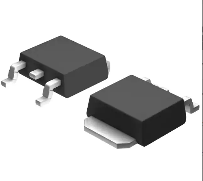


 工商网监
湘ICP备2023018690号
工商网监
湘ICP备2023018690号

