MH248
Specifications
Micropower Hall Effect Switch
MH248 Hall-effect sensor is a temperature stable, stress-resistant , micro-power switch.
Superior high-temperature performance is made possible through a dynamic offset cancellation
that utilizes chopper-stabilization. This method reduces the offset voltage normally caused by
device over molding, temperature dependencies, and thermal stress.
MH248 includes the following on a single silicon chip: voltage regulator, Hall voltage
generator, small-signal amplifier, chopper stabilization, Schmitt trigger, open-drain output.
Advanced CMOS wafer fabrication processing is used to take advantage of low-voltage
requirements, component matching, very low input-offset errors, and small component
geometries.
This device requires the presence of omni-polar magnetic fields for operation.
MH248 is rated for operation between the ambient temperatures –40℃ and + 85℃ for
the E temperature range. The four package styles available provide magnetically optimized
solutions for most applications. Package types SO is an SOT-23(1.1 mm nominal height),SQ is
an QFN2020-3(0.5 mm nominal height),Tsot-23 is an ST(0.7 mm nominal height) ,a miniature
low-profile surface-mount package, while package UA is a three-lead ultra-mini SIP for
through-hole mounting.
The package type is in a lead Halogen Free version was verified by third party Lab.
Features and Benefits
CMOS Hall IC Technology
Solid-State Reliability
Micro power consumption for battery-powered applications
Omni polar, output switches with absolute value of North or South pole from magnet
Operation down to 2.5 V and Max at 3.5V.
High Sensitivity for direct reed switch replacement applications
Multi Small Size option
Custom sensitivity selection is available in optional package.
Pb Free/Green chip is qualified by third party lab.
Applications
Solid state switch
Handheld Wireless Handset Awake Switch ( Flip Cell/PHS Phone/Note Book/Flip
Video Set)
Lid close sensor for battery powered devices
Magnet proximity sensor for reed switch replacement in low duty cycle applications
032315
Page 1 of 6
Rev. 1.04
�MH248
Specifications
Micropower Hall Effect Switch
Ordering Information
XXXXXXXXX - X
Company Name and Product Category
MH:MST Hall Effect/MP:MST Power IC
Part number
Sorting Code
181,182,183,184,185,248,249,276,477,381,381F,381R,382…..
If part # is just 3 digits, the forth digit will be omitted.
Package type
Temperature range
Temperature Code
E: 85 ℃, I: 105 ℃, K: 125 ℃, L: 150 ℃
Package type
Part number
UA:TO-92S,VK:TO-92S(4pin),VF:TO-92S(5pin),SO:SOT-23,
Company Name and Product Category
SQ:QFN-3,ST:TSOT-23,SN:SOT-553,SF:SOT-89(5pin),
SS:TSOT-26,SD:DFN-6
Sorting
α,β,Blank…..
Part No.
MH248EUA
MH248ESO
MH248EST
Temperature Suffix
E (-40℃ to + 85℃)
E (-40℃ to + 85℃)
E (-40℃ to + 85℃)
Package Type
UA (TO-92S)
SO (SOT-23)
ST (TSOT-23)
MH248ESQ
MH248ESO-α
MH248ESO-β
MH248ESO-γ
E
E
E
E
SQ
SO
SO
SO
(-40℃
(-40℃
(-40℃
(-40℃
to
to
to
to
+
+
+
+
85℃)
85℃)
85℃)
85℃)
(QFN2020-3)
(SOT-23)
(SOT-23)
(SOT-23)
Custom sensitivity selection is available by MST sorting technology
Functional Diagram
VDD
Awake/Sleep
Timing Control
Out
Offset
Cancellation
Control
Logic
Amp
Hall
Sensor
GND
Note: Static sensitive device; please observe ESD precautions. Reverse V DD protection is not included. For reverse
voltage protection, a 100Ω resistor in series with VDD is recommended.
032315
Page 2 of 6
Rev. 1.04
�MH248
Specifications
Micropower Hall Effect Switch
Absolute Maximum Ratings At (Ta=25℃)
Characteristics
Values
Unit
Supply voltage,(VDD)
5
V
Output Voltage,(Vout)
5
V
-0.3
V
Unlimited
Gauss
2
mA
Operating temperature range, (Ta)
-40 to +85
℃
Storage temperature range, (Ts)
-55 to +150
℃
Maximum Junction Temp,(Tj)
150
℃
(θJA) UA / SO / ST / SQ
206 / 543 / 310 / 543
℃/W
(θJC) UA / SO / ST /SQ
148 / 410 / 223 / 410
℃/W
Package Power Dissipation, (PD) UA / SO / ST / SQ
606 / 230 / 400 / 230
mW
Reverse voltage, (VDD) (VOUT)
Magnetic flux density
Output current(IOUT)
Thermal Resistance
Note: Exceeding the absolute maximum ratings may cause permanent damage. Exposure to absolute maximumrated conditions for extended periods may affect device reliability.
Electrical Specifications
DC Operating Parameters TA=+25℃, VDD=3.0V
Parameters
Test Conditions
Supply Voltage,(VDD)
Operating
Supply Current,(IDD)
Min
Typ
2.5
Max
Units
3.5
V
Awake State
2.5
4.0
mA
Sleep State
8.0
12
μA
Average
10
16
μA
Output Leakage Current,(Ioff)
Output off
1
uA
Output Low Voltage,(Vsat)
IOUT=1mA
0.3
V
Awake mode time,(Taw)
Operating
70
uS
Sleep mode time,(TSL)
Operating
70
mS
0.1
%
Duty Cycle,(D,C)
Operate Point,
Release Point
Hysteresis,(BHYS)
032315
(BOPS)
S pole to branded side, B > BOP, Vout On
6
60
(BOPN)
N pole to branded side, B > BOP, Vout On
-60
-6
(BRPS)
S pole to branded side, B < BRP, Vout Off
5
59
(BRPN)
N pole to branded side, B < BRP, Vout Off
-60
-5
|BOPx - BRPx|
Page 3 of 6
7
Gauss
Gauss
Gauss
Rev. 1.04
�MH248
Specifications
Micropower Hall Effect Switch
Typical Application circuit
Vcc
C1:10nF
C2:100pF
R1:100KΩ
R1
VDD
MH182
MH248
C1
Out
Out
GND
C2
Sensor Location, Package Dimension and Marking
MH248 Package
UA Package
Hall Chip location
2.00
0.9
248
XXX
Hall Sensor
Location
NOTES:
Mark
1).Controlling dimension:
mm 2).Leads must be free
of flash
Output Pin Assignment
(Top view)
and plating voids
3).Do not bend leads within
248
XXX
1 mm of lead to package
interface.
4).PINOUT:
032315
Pin 1
VDD
Pin 2
GND
Pin 3
Output
Page 4 of 6
1
VDD
2
GND
3
Out
Rev. 1.04
�MH248
Specifications
Micropower Hall Effect Switch
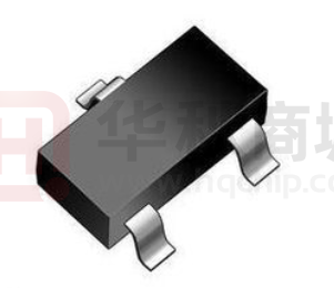
SO Package
Hall Plate Chip Location
(Top View)
(Bottom view)
3
3
0.80
248XX
1
2
2
1
Hall Sensor
Location
1.45
NOTES:
1. PINOUT (See Top View at left :)
Pin 1
VDD
Pin 2
Output
Pin 3
GND
2. Controlling dimension: mm
3. Lead thickness after solder plating
will be 0.254mm maximum
ST Package (TSOT-23)
(Top View)
Hall Plate Chip Location
(Bottom view)
3
3
0.80
248XX
1
2
2
Hall Sensor
Location
1
1.45
NOTES:
1.
2.
032315
PINOUT (See Top View at left:)
Pin 1
VDD
Pin 2
Output
Pin 3
GND
Controlling dimension: mm;
Page 5 of 6
Rev. 1.04
�MH248
Specifications
Micropower Hall Effect Switch
SQ Package
Hall Plate Chip Location
248
XX
(Top view)
NOTES:
3.
1
3
PINOUT (See Top View
at left)
1
2
4.
Pin 1
VDD
Pin 2
Output
Pin 3
GND
1
Hall Sensor
Location
1
2
Controlling dimension:
mm;
5.
3
Chip rubbing will be
10mil
6.
maximum;
Chip must be in PKG.
center.
032315
Page 6 of 6
Rev. 1.04
�


 工商网监
湘ICP备2023018690号
工商网监
湘ICP备2023018690号
