ASDM80R055NTD
80V N-Channel MOSFET
Features
Product Summary
•�Optimized�for�chargers
•�100%�avalanche�tested
•�Superior�thermal�resistance
•�N-channel,�Logic�level
•�Pb-free�lead��plating;�RoHS�compliant
•�Halogen-free�according�to�IEC61249-2-21
•�Ideal�for�high-frequency�switching
VDSS
80
V
RDS(ON)-Typ@VGS=10V
5.4
mΩ
ID
40
A
Product�validation
Qualified�according�to�JEDEC�Standard
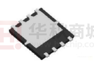
DFN3*3-8
�Maximum�ratings at TA=25�°C, unless otherwise specified
Parameter
Symbol
Continuous drain current
Values
Unit
Note�/�Test�Condition
40
40
14
A
VGS=10�V,�TC=25�°C
VGS=10�V,�TC=100�°C
VGS=10�V,�TA=25�°C,�RthJA�=60K/W1)
-
160
A
TC=25�°C
-
-
38
mJ
ID=20�A,�RGS=25�Ω
VGS
-20
-
20
V
-
Power dissipation
Ptot
-
-
46
2.1
W
TC=25�°C
TA=25�°C,�RthJA=60�K/W1)
Operating and storage temperature
Tj,�Tstg
-55
-
150
°C
IEC climatic category;
DIN IEC 68-1: 55/150/56
Unit
Note�/�Test�Condition
Min.
Typ.
Max.
ID
-
-
ID,pulse
-
Avalanche energy, single pulse
EAS
Gate source voltage
Pulsed drain current2)
3)
�Thermal�characteristics
Parameter
Symbol
Thermal resistance, junction - case
Values
Min.
Typ.
Max.
RthJC
-
1.6
2.7
K/W
-
Device on PCB,
minimal footprint
RthJA
-
-
62
K/W
-
Device on PCB,
6 cm2 cooling area1)
RthJA
-
-
60
K/W
-
DEC 2018 Version1.0
1/10
Ascend Semicondutor Co.,Ltd
�ASDM80R055NTD
80V N-Channel MOSFET
Electrical�characteristics at�Tj=25�°C,�unless�otherwise�specified
Static�characteristics
Parameter
Symbol
Drain-source breakdown voltage
Values
Unit
Note�/�Test�Condition
-
V
VGS=0�V,�ID=1�mA
1.7
2.3
V
VDS=VGS,�ID=20�µA
-
0.1
10
1
100
µA
VDS=80�V,�VGS=0�V,�Tj=25�°C
VDS=80�V,�VGS=0�V,�Tj=125�°C
IGSS
-
10
100
nA
VGS=20�V,�VDS=0�V
Drain-source on-state resistance
RDS(on)
-
5.4
7.3
6.5
9.4
mΩ
VGS=10�V,�ID=20�A
VGS=4.5�V,�ID=10�A
Gate resistance1)
RG
-
1.2
1.8
Ω
-
Transconductance
gfs
25
50
-
S
|VDS|>2|ID|RDS(on)max,�ID=20�A
Unit
Note�/�Test�Condition
Min.
Typ.
Max.
V(BR)DSS
80
-
Gate threshold voltage
VGS(th)
1.1
Zero gate voltage drain current
IDSS
Gate-source leakage current
�Dynamic�characteristics
Parameter
Symbol
Values
Min.
Typ.
Ciss
-
1400
1800
pF
VGS=0�V,�VDS=40�V,�f=1�MHz
Coss
-
300
390
pF
VGS=0�V,�VDS=40�V,�f=1�MHz
Crss
-
16
28
pF
VGS=0�V,�VDS=40�V,�f=1�MHz
Turn-on delay time
td(on)
-
5.0
-
ns
VDD=40�V,�VGS=10�V,�ID=20�A,
RG,ext=1.6�Ω
Rise time
tr
-
2.9
-
ns
VDD=40�V,�VGS=10�V,�ID=20�A,
RG,ext=1.6�Ω
Turn-off delay time
td(off)
-
14
-
ns
VDD=40�V,�VGS=10�V,�ID=20�A,
RG,ext=1.6�Ω
Fall time
tf
-
2.6
-
ns
VDD=40�V,�VGS=10�V,�ID=20�A,
RG,ext=1.6�Ω
Unit
Note�/�Test�Condition
Input capacitance1)
Output capacitance
1)
Reverse transfer capacitance
1)
Max.
�Gate�charge�characteristics2)
Parameter
Symbol
Gate to source charge
Gate charge at threshold
Values
Min.
Typ.
Max.
Qgs
-
4.1
-
nC
VDD=40�V,�ID=20�A,�VGS=0�to�4.5�V
Qg(th)
-
2.3
-
nC
VDD=40�V,�ID=20�A,�VGS=0�to�4.5�V
Gate to drain charge
Qgd
-
3.3
4.9
nC
VDD=40�V,�ID=20�A,�VGS=0�to�4.5�V
Switching charge
Qsw
-
5.1
-
nC
VDD=40�V,�ID=20�A,�VGS=0�to�4.5�V
Gate charge total
Qg
-
10
13
nC
VDD=40�V,�ID=20�A,�VGS=0�to�4.5�V
Gate plateau voltage
Vplateau
-
2.9
-
V
VDD=40�V,�ID=20�A,�VGS=0�to�4.5�V
Gate charge total, sync. FET
Qg(sync)
-
18
-
nC
VDS=0.1�V,�VGS=0�to�10�V
Qoss
-
19
26
nC
VDD=40�V,�VGS=0�V
1)
1)
1)
Output charge
1)
2)
Defined by design. Not subject to production test
See ″Gate charge waveforms″ for parameter definition
DEC 2018 Version1.0
2/10
Ascend Semicondutor Co.,Ltd
�ASDM80R055NTD
80V N-Channel MOSFET
Reverse�diode
Parameter
Symbol
Diode continuous forward current
Diode pulse current
Diode forward voltage
1)
Reverse recovery time
1)
Reverse recovery charge
DEC 2018 Version1.0
Values
Unit
Note�/�Test�Condition
39
A
TC=25�°C
-
156
A
TC=25�°C
-
0.83
1.2
V
VGS=0�V,�IF=20�A,�Tj=25�°C
trr
-
18
36
ns
VR=40�V,�IF=20�A,�diF/dt=100�A/µs
Qrr
-
7
14
nC
VR=40�V,�IF=20�A,�diF/dt=100�A/µs
Min.
Typ.
Max.
IS
-
-
IS,pulse
-
VSD
3/10
Ascend Semicondutor Co.,Ltd
�ASDM80R055NTD
80V N-Channel MOSFET
Electrical�characteristics�diagrams
Diagram�1:�Power�dissipation
Diagram�2:�Drain�current
50
40
40
30
30
ID�[A]
Ptot�[W]
50
20
20
10
10
0
0
25
50
75
100
125
150
0
175
0
25
50
75
TC�[°C]
100
125
Ptot=f(TC)
ID=f(TC);�VGS≥10�V
Diagram�3:�Safe�operating�area
Diagram�4:�Max.�transient�thermal�impedance
103
175
101
102
1 µs
0.5
10 µs
100
101
0.2
ZthJC�[K/W]
100 µs
ID�[A]
150
TC�[°C]
1 ms
DC
10 ms
0.1
0.05
10-1
0.02
100
0.01
single pulse
10-1
10-1
100
101
102
10-2
10-6
10-5
VDS�[V]
10-3
10-2
tp�[s]
ID=f(VDS);�TC=25�°C;�D=0;�parameter:�tp
DEC 2018 Version1.0
10-4
ZthJC=f(tp);�parameter:�D=tp/T
4/10
Ascend Semicondutor Co.,Ltd
10-1
�ASDM80R055NTD
80V N-Channel MOSFET
Diagram�5:�Typ.�output�characteristics
Diagram�6:�Typ.�drain-source�on�resistance
160
15
10 V
140
5V
4.5 V
120
10
4V
RDS(on)��[mΩ]
100
ID�[A]
4V
80
60
4.5 V
5V
5.5 V
6V
7V
10 V
5
3.5 V
40
3.2 V
3V
20
2.8 V
0
0.0
0.5
1.0
1.5
0
2.0
0
40
80
VDS�[V]
120
160
ID�[A]
ID=f(VDS);�Tj=25�°C;�parameter:�VGS
RDS(on)=f(ID);�Tj=25�°C;�parameter:�VGS
Diagram�7:�Typ.�transfer�characteristics
Diagram�8:�Typ.�forward�transconductance
160
80
140
120
60
gfs�[S]
ID�[A]
100
80
40
60
40
20
150 °C
20
0
0
2
25 °C
4
6
8
0
0
VGS�[V]
40
ID�[A]
ID=f(VGS);�|VDS|>2|ID|RDS(on)max;�parameter:�Tj
DEC 2018 Version1.0
20
gfs=f(ID);�Tj=25�°C
5/10
Ascend Semicondutor Co.,Ltd
60
�ASDM80R055NTD
80V N-Channel MOSFET
Diagram�9:�Drain-source�on-state�resistance
Diagram�10:�Typ.�gate�threshold�voltage
14
3
12
10
2
RDS(on)�[mΩ]
6
200 µA
VGS(th)�[V]
max
8
typ
20 µA
1
4
2
0
-60
-20
20
60
100
140
0
-60
180
-20
20
Tj�[°C]
60
100
140
180
Tj�[°C]
RDS(on)=f(Tj);�ID=20�A;�VGS=10�V
VGS(th)=f(Tj);�VGS=VDS
Diagram�11:�Typ.�capacitances
Diagram�12:�Forward�characteristics�of�reverse�diode
4
103
10
25 °C
25 °C, max
150 °C
150 °C, max
Ciss
102
IF�[A]
C�[pF]
103
Coss
102
101
Crss
101
0
20
40
60
100
0.0
0.5
VDS�[V]
C=f(VDS);�VGS=0�V;�f=1�MHz
DEC 2018 Version1.0
1.0
1.5
VSD�[V]
IF=f(VSD);�parameter:�Tj
6/10
Ascend Semicondutor Co.,Ltd
2.0
�ASDM80R055NTD
80V N-Channel MOSFET
Diagram�13:�Avalanche�characteristics
Diagram�14:�Typ.�gate�charge
2
10
10
9
8
7
25 °C
101
100 °C
12 V
6
VGS�[V]
IAV�[A]
30 V
125 °C
48 V
5
4
0
10
3
2
1
10-1
100
101
102
103
tAV�[µs]
0
0
4
8
12
16
20
Qgate�[nC]
IAS=f(tAV);�RGS=25�Ω;�parameter:�Tj(start)
VGS=f(Qgate);�ID=20�A�pulsed;�parameter:�VDD
Diagram�15:�Drain-source�breakdown�voltage
Diagram Gate charge waveforms
70
66
VBR(DSS)�[V]
62
58
54
50
-60
-20
20
60
100
140
180
Tj�[°C]
VBR(DSS)=f(Tj);�ID=1�mA
DEC 2018 Version1.0
7/10
Ascend Semicondutor Co.,Ltd
24
�ASDM80R055NTD
80V N-Channel MOSFET
Ordering and Marking Information
Ordering Device No.
Marking
Package
Packing
Quantity
ASDM80R055NTD-R
80R055N
DFN3*3-8
Tape&Reel
5000/Reel
MARKING
PACKAGE
DFN3*3-8
DEC 2018 Version1.0
80R055N
8/10
Ascend Semicondutor Co.,Ltd
�ASDM80R055NTD
80V N-Channel MOSFET
Package�Outlines
DFN3*3-8
PACKAGE - GROUP
NUMBER:
REVISION: 03
DIMENSIONS
A
b
c
D
D1
D2
E
E1
E2
e
L
L1
L2
aaa
DEC 2018 Version1.0
PG-TSDSON-8-U03
DATE: 20.10.2020
MILLIMETERS
MIN.
MAX.
0.90
1.10
0.24
0.44
(0.20)
3.20
3.40
2.19
2.39
1.54
1.74
3.20
3.40
2.01
2.21
0.10
0.30
0.65
0.30
0.50
0.40
0.60
0.50
0.70
0.06
9/10
Ascend Semicondutor Co.,Ltd
�ASDM80R055NTD
80V N-Channel MOSFET
IMPORTANT NOTICE
Xi‘an Ascend Semiconductor incorporated MAKES NO WARRANTY OF ANY KIND, EXPRESS OR IMPLIED, WITH REGARDS TO THIS
DOCUMENT, INCLUDING, BUT NOT LIMITED TO, THE IMPLIED WARRANTIES OF MERCHANTABILITY AND FITNESS FOR A PARTICULAR
PURPOSE (AND THEIR EQUIVALENTS UNDER THE LAWS OF ANY JURISDICTION).
Xi‘an Ascend Semiconductor Incorporated and its subsidiaries reserve the right to make modifications, enhancements, improvements, corrections
or other changes without further notice to this document and any product described herein. Xi‘an Ascend Semiconductor Incorporated does not
assume any liability arising out of the application or use of this document or any product described herein; neither does Xi‘an Ascend
Semiconductor Incorporated convey any license under its patent or trademark rights, nor the rights of others. Any Customer or user of this
document or products described herein in such applications shall assume .
all risks of such use and will agree to hold Ascendsemi Incorporated and all the companies whose products are represented on Xi‘an
Ascend Semiconductor Incorporated website, harmless against all damages.
Xi‘an Ascend Semiconductor Incorporated does not warrant or accept any liability whatsoever in respect of any products purchased through
unauthorized sales channel. Should Customers purchase or use Xi‘an Ascend Semiconductor Incorporated products for any unintended or
unauthorized application, Customers shall indemnify and hold Xi‘an Ascend Semiconductor Incorporated and its representatives harmless against
all claims, damages, expenses, and attorney fees arising out of, directly or indirectly, any claim of personal injury or death associated with such
unintended or unauthorized application.
www.ascendsemi.com
DEC 2018 Version1.0
10/10
Ascend Semicondutor Co.,Ltd
�


 工商网监
湘ICP备2023018690号
工商网监
湘ICP备2023018690号
