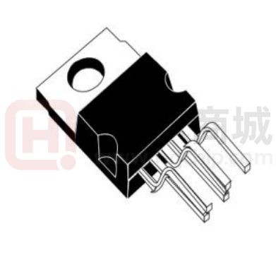
XBLW TDA2050
32W Hi-Fi AUDIO POWER AMPLIFIER
General Description
The XBLW TDA2050 is a monolithic integrated circuit in Pentawatt package, intended for use as an audio class AB
audio amplifier. Thanks to its high power capability the TDA2050 is able to provide up to 35W true rms power into 4
ohm load @ THD = 10%, VS =18V, f = 1KHz and up to 32W into 8ohm load @ THD = 10%, VS =
22V, f =
1KHz.Moreover, the TDA 2050 delivers typically 50W music power into 4 ohm load over 1 sec at VS= 22.5V, f =
1KHz.
The high power and very low harmonic and cross- over distortion (THD = 0.05% typ, @ VS = 22V, PO = 0. 1 to 15W,
RL=8ohm, f=100Hz to 15KHz) make the device most suitable for both HiFi and high class TV sets.
General Description
High Output Power(40W Music Power Iec 268.3 Rules )High Operating Supply Voltage (50V)
Single Or Split Supply Operations
Very Low Distortion
Short Circuit Protection (Out To Gnd)
Thermal Shutdown
Ordering Information
Product Model
XBLW TDA2050A
XBLW TDA2050A
Package Type
TO-220-5L
TO-263-5L
Marking
TDA2050A
TDA2050A
Packing
Packing Qty
Tube
Tape
1000/Box
500/Reel
PIN CONNECTION (Top view)
SCHEMATIC DIAGRAM
XBLWversion1.0
文档仅供参考,实际应用测试为准
www.xinboleic.com
技术支持热线:4009682003
第 1 页 共 14 页
�XBLW TDA2050
32W Hi-Fi AUDIO POWER AMPLIFIER
TEST AND APPLICATION CIRCUIT
ABSOLUTE MAXIMUM RATINGS
Symbol
Parameter
VS
Supply Voltage
Vi
Input Voltage
Vi
Differential Input Voltage
IO
Ptot
Value
Unit
V
25
VS
15
V
Output Peak Current (internally limited)
5
A
25
W
Tstg, Tj
Power Dissipation TCASE = 75。C
Storage and Junction Temperature
-40 to 150
。C
TL
Lead Temperature (Soldering, 10 seconds)
245
。C
THERMAL DATA
Symbol
Rth jcase
XBLWversion1.0
Description
Thermal Resistance junction-case
Max
文档仅供参考,实际应用测试为准
www.xinboleic.com
技术支持热线:4009682003
Value
Unit
3
。C/W
第 2 页 共 14 页
�XBLW TDA2050
32W Hi-Fi AUDIO POWER AMPLIFIER
ELECTRICAL CHARACTERISTICS
(Refer to the Test Circuit, VS = 土18V, Tamb = 25。C, f = 1 kHz; un-less otherwise specified)
Symbol
VS
Id
Parameter
Test Condition
Supply Voltage Range
Min.
Typ.
土4.5
Unit
土25
V
VS = 土4.5V
30
50
mA
VS = 土25V
55
90
mA
Input Bias Current
VS = 土22V
0.1
0.5
µA
VOS
Input Offset Voltage
VS = 土22V
土15
mV
IOS
Input Offset Current
VS = 土22V
土200
nA
Ib
Quiescent Drain Current
Max.
d = 0.5%
28
W
18
W
25
W
RL = 4Ω
35
W
RL = 8Ω
22
W
VS = 土22V RL = 8Ω
32
W
50
W
24
RL = 4Ω
RL = 8Ω
VS = 土22V RL = 8Ω
RMS Output Power
22
d = 10%
PO
Music Power
d = 10%; T = 1s
IEC268.3 RULES
VS = 土22.5V; RL = 4
RL = 4
f = 1kHz, PO = 0. 1 to 24W
d
Total Harmonic Distortion
0.03
f = 100Hz to 10kHz, PO = 0. 1 to
18W
VS =土22V RL = 8
f = 1kHz, PO = 0. 1 to 20W
Slew Rate
GV
GV
Open Loop Voltage Gain
Closed Loop Voltage Gain
BW
Power Bandwidth (-3dB)
eN
Total Input Noise
Ri
Input Resistance (pin 1)
SVR
Supply Voltage Rejection
η
Efficiency
30
%
%
%
8
V/µs
80
dB
30.5
31
20 to
RL = 4ΩVi = 200mV
curve A
4
B = 22Hz to 22kHz
5
500
dB
Hz
80,000
µV
10
µV
kΩ
Rs = 22kΩ; f = 100Hz;
Vripple = 0.5Vrms
45
dB
PO = 28W; RL = 4Ω
65
%
67
%
150
。C
PO = 25W; RL = 8Ω;
Thermal Shut-down
Junction Temperature
XBLWversion1.0
0.5
0.5
5
VS = 土22V
Tsd-j
%
0.02
f = 100Hz to 10kHz, PO = 0. 1 to
15W
SR
0.5
文档仅供参考,实际应用测试为准
www.xinboleic.com
技术支持热线:4009682003
第 3 页 共 14 页
�XBLW TDA2050
32W Hi-Fi AUDIO POWER AMPLIFIER
Figure 1: Split Supply Typical Application Circuit
TDA2050
Figure 2: P.C. Board and ComponentsLayout of the Circuit of Fig. 1 (1:1)
XBLWversion1.0
文档仅供参考,实际应用测试为准
www.xinboleic.com
技术支持热线:4009682003
第 4 页 共 14 页
�XBLW TDA2050
32W Hi-Fi AUDIO POWER AMPLIFIER
SPLIT SUPPLY APPLICATION SUGGESTIONS
The recommended values of the external components are those shown on the application circuit of fig. 2.
Different values can be used. The following table can help the designer.
Component
Recommende
Purpose
d
Larger than
Smaller than
Recommended Value
Recommended Value
Value
R1
22kΩ
R2
680
R3
22k
R4
2.2
C1
1µF
C2
22µF
C3
Input Impedance
Feedback Resistor
Frequency Stability
Increase of Input
Decrease of Input
Impedance
Impedance
Decrease of Gain (*)
Increase of Gain
Increase of Gain
Decrease of Gain (*)
Danger of Oscillations
Input Decoupling DC
Higher Lowfrequency cut-off
Inverting Input
Increase of Switch
DC Decoupling
ON/OFF Noise
Higher Lowfrequency cut-off
100nF
Supply Voltage Bypass
Danger of Oscillations
220µF
Supply Voltage Bypass
Danger of Oscillations
0.47µF
Frequency Stability
Danger of Oscillations
C4
C5
C6
C7
(*) The gain must be higher than 24dB
PRINTED CIRCUIT BOARD
The layout shown in fig. 2 should be adopted by the designers. If different layouts are used, the ground points of input
1 and input 2 must be well decoupled from the ground return of the output in which a high current flows.
Figure 3: Single Supply Typical Application Circuit
TDA2050
XBLWversion1.0
文档仅供参考,实际应用测试为准
www.xinboleic.com
技术支持热线:4009682003
第 5 页 共 14 页
�XBLW TDA2050
32W Hi-Fi AUDIO POWER AMPLIFIER
Figure 4: P.C. Board and ComponentsLayout of the Circuit of Fig. 3 (1:1)
SINGLE SUPPLY APPLICATION SUGGESTIONS
The recommended values of the external components are those shown on the application circuit of fig. 3.
Different values can be used. The following table can help the designer.
Component
Recommende
d
Purpose
Larger than
Smaller than
Recommended Value
Recommended Value
Value
R1,R2,R3
22KΩ
Biasing Resistor
R4
22KΩ
Feedback Resistors
R5
680
R6
2.2
Frequency Stability
C1
2.2µF
Input Decoupling DC
C2
100µF
Supply Voltage Rejection
Increase of Gain
Decrease of Gain (*)
Decrease of Gain (*)
Increase of Gain
Danger of Oscillations
Higher Lowfrequency cut-off
Worse Turn-off Transient
Worse Turn-on Delay
C3
1000µF
Supply Voltage Bypass
Danger of
Oscillations Worse
of Turn-off
Transient
C4
C5
22µF
Inverting Input DC
Increase of Switching
Decoupling
ON/OFF
Higher Lowfrequency cut-off
100nF
Supply Voltage Bypass
Danger of Oscillations
C6
0.47µF
Frequency Stability
Danger of Oscillations
C7
1000µF
Output DC Decoupling
Higher Lowfrequency cut-off
XBLWversion1.0
文档仅供参考,实际应用测试为准
www.xinboleic.com
技术支持热线:4009682003
第 6 页 共 14 页
�XBLW TDA2050
32W Hi-Fi AUDIO POWER AMPLIFIER
(*) The gain must be higher than 24 dB
NOTE
If the supply voltage is lower than 40V and the load is 8ohm (or more) a lower value of C2 can be used (i.e. 22µF). C7 can be
larger than 1000uF only if the supply voltage does not exceed 40V.
TYPICAL CHARACTERISTICS (Split Supply Test Circuit unless otherwise specified)
Figure 5: Output Power vs. Supply Voltage
Figure 6: Distortion vs. Output Power
Figure 7: Output Power vs. Supply Voltage
Figure 8: Distortion vs. Output Power
XBLWversion1.0
文档仅供参考,实际应用测试为准
www.xinboleic.com
技术支持热线:4009682003
第 7 页 共 14 页
�XBLW TDA2050
32W Hi-Fi AUDIO POWER AMPLIFIER
Figure. 9: Distortion vs. Frequency
XBLWversion1.0
Figure 10: Distortion vs. Frequency
文档仅供参考,实际应用测试为准
www.xinboleic.com
技术支持热线:4009682003
第 8 页 共 14 页
�XBLW TDA2050
32W Hi-Fi AUDIO POWER AMPLIFIER
SHORT CIRCUIT PROTECTION
The TDA2050 has an original circuit which limits the current of the output transistors. The maximum output
current is a function of the collector emitter voltage; hence the output transistors work within their safe
operating area. This function can therefore be considered as being peak power limiting rather than simple current
limiting.
It reduces the possibility that the device gets damaged during an accidental short circuit from AC output to ground.
THERMAL SHUTDOWN
The presence of a thermal limiting circuit offers the following advantages:
1)An overload on the output (even if it is permanent), or an above limit ambient temperature can be easily
tolerated since the Tj cannot be higher than 150°C.
2)The heat sink can have a smaller factor of safety compared with that of a conventional circuit. There is no
possibility of device damage due to high junction temperature. If for any reason, the junction temperature
increases up to 150°C, the thermal shutdown simply reduces the power dissipation and the current
consumption.
The maximum allowable power dissipation depends upon the thermal resistance junction-ambient. Fig. 17 shows
this dissipable power as a function of ambient temperature for different thermal resistance.
XBLWversion1.0
文档仅供参考,实际应用测试为准
www.xinboleic.com
技术支持热线:4009682003
第 9 页 共 14 页
�XBLW TDA2050
32W Hi-Fi AUDIO POWER AMPLIFIER
Figure 17: Maximum Allowable Power Dissipation vs. Ambient Temperature
MOUNTING INSTRUCTIONS
The power dissipated in the circuit must be removed by adding an external heat sink.
Thanks to the PENTAWATT package, the heat sink mounting operation is very simple, a screw or a
compression spring (clip) being sufficient. Between the heat sink and the package is better to insert a layer of silicon
grease, to optimize the thermal contact; no electrical isolation is needed between the two surfaces. Fig. 18 shows an
example of heat sink.
Dimension suggestion
The following table shows the length that the heat sink in fig. 18 must have for several values of Ptot
and Rth
Figure 18: Example of heat-sink
APPENDIX A
A.1 - MUSIC POWER CONCEPT
MUSIC POWER is (according to the IEC clauses n.268-3 of Jan 83) the maximum power which the amplifier is
capable of producing across the rated load resistance (regardless of non linearity) 1 sec after the application of a
sinusoidal input signal of frequency 1 KHz.
According to this definition our method of measurement comprises the following steps:
Set the voltage supply at the maximum operating value;
XBLWversion1.0
文档仅供参考,实际应用测试为准
www.xinboleic.com
技术支持热线:4009682003
第 10 页 共 14 页
�XBLW TDA2050
32W Hi-Fi AUDIO POWER AMPLIFIER
- Apply a input signal in the form of a 1KHz tone burst of 1 sec duration: the repetition period of the signal pulses
is 60 sec;
Ptot (W)
12
8
6
Lenght of heat sink (mm)
60
40
30
Rth of heat sink (。C/W)
4.2
6.2
8.3
- The output voltage is measured 1 sec from the start of the pulse;
- Increase the input voltage until the output signal shows a THD=1 0 %;
- The music power is then V2 out /RL, where Vout is the output voltage measured in the condition of point 4 and RL is
the rated load impedance;
The target of this method is to avoid excessive dissipation in the amplifier.
A.2 - INSTANTANEOUS POWER
Another power measurement (MAXIMUM INSTANTANEOUS OUTPUT POWER) was proposed by IEC in
1988 (IEC publication 268-3 subclause 19.A).
We give here only a brief extract of the concept, and a circuit useful for the measurement. The
supply voltage is set at the maximum operating value.
The test signal consists of a sinusoidal signal whose frequency is 20 Hz, to which are added alternate
positive and negative pulses of 50 µs duration and 500 Hz repetition rate. The amplitude of the 20 Hz
signal is chosen to drive the amplifier to its voltage clipping limits, while the amplitude of the
pulses takes the amplifier alternately into its current-overload limits
A circuit for generating the test signal is given in fig. 19.
The load network consists of a 40 F capacitor, in series with a 1 ohm resistor. The capacitor limits the current due to
the 20 Hz signal to a low value, whereas for he short pulses the effective load impedance is of the order of 1 ohm , and
a high output current is produced.
Using this signal and load network the measurement may be made without causing excessive dissipation in the
amplifier. The dissipation in the 1 ohm resistor is much lower than a rated output power of the amplifier,
because the duty-cycle of the high output current is low.
By feeding the amplifier output voltage to the Xplates of an oscilloscope, and the voltage across the 1 ohm resistor
(representing the output current) to the Y=plates, it is possible to read on the display the value of the maximum
instantaneous output power.
The result of this test applied at the TDA 2050 is:
PEAK POWER = 100W typ
Figure 19: Test circuit for peak power measurement
XBLWversion1.0
文档仅供参考,实际应用测试为准
www.xinboleic.com
技术支持热线:4009682003
第 11 页 共 14 页
�XBLW TDA2050
32W Hi-Fi AUDIO POWER AMPLIFIER
Physical Dimensions
TO-220-5L
Dimensions In Millimeters(TO220-5L)
A
A1
B
C
C1
D
E
F
L1
L2
L3
L4
a
b
e
Min:
4.45
1.22
10
8.45
6.10
0.32
4.24
8.24
15.45
17.65
3.00
2.64
0.76
1.70
2.67
Max:
4.62
1.32
10.4
8.95
6.60
0.42
4.70
8.70
16.25
18.25
3.85
2.84
1.02
BSC
TYP
Symbol:
XBLWversion1.0
文档仅供参考,实际应用测试为准
www.xinboleic.com
技术支持热线:4009682003
第 12 页 共 14 页
�XBLW TDA2050
32W Hi-Fi AUDIO POWER AMPLIFIER
TO-263-5L Unit:mm
XBLWversion1.0
文档仅供参考,实际应用测试为准
www.xinboleic.com
技术支持热线:4009682003
第 13 页 共 14 页
�XBLW TDA2050
32W Hi-Fi AUDIO POWER AMPLIFIER
Statement:
Shenzhen xinbole electronics co., ltd. reserves the right to change the product specifications, without notice!
Before placing an order, the customer needs to confirm whether the information obtained is the latest version,
and verify the integrity of the relevant information.
Any semiconductor product is liable to fail or malfunction under certain conditions, and the buyer shall be
responsible for complying with safety standards in the system design and whole machine manufacturing using
Shenzhen xinbole electronics co., ltd products, and take appropriate security measures to avoid the potential risk
of failure may result in personal injury or property losses of the situation occurred!
Product performance is never ending, Shenzhen xinbole electronics co., ltd will be dedicated to provide
customers with better performance, better quality of integrated circuit products.
XBLWversion1.0
文档仅供参考,实际应用测试为准
www.xinboleic.com
技术支持热线:4009682003
第 14 页 共 14 页
�


 工商网监
湘ICP备2023018690号
工商网监
湘ICP备2023018690号
