1N5818-1, 1N5819-1, 1N6759-1 – 1N6761-1
and DSB1A20 – DSB1A100
Available on
commercial
versions
1 Amp Schottky Barrier Rectifiers
Qualified per MIL-PRF-19500/586
Qualified Levels*:
JAN, JANTX, JANTXV
and JANS
DESCRIPTION
This 1 Amp Schottky barrier rectifier is metallurgically bonded and offers military grade
qualifications for the part numbers of 1N5819-1 and 1N6761-1 for high-reliability applications.
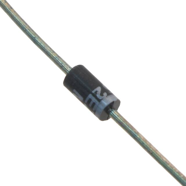
This small diode is hermetically sealed and bonded into a DO-41 glass package.
Important: For the latest information, visit our website http://www.microsemi.com.
FEATURES
•
JEDEC registered 1N5818, 1N5819 and 1N6759 through 1N6761 numbers.
•
Hermetically sealed DO-41 glass package.
DO-41 Package
•
Metallurgically bonded.
•
*1N5819-1 and 1N6761-1 only are available in JAN, JANTX, JANTXV and JANS qualifications per
MIL-PRF-19500/586.
(See part nomenclature for all available options.)
•
Also available in:
DO-213AB package
(surface mount)
1N5819UR-1,
1N6761UR-1 and CDLL
variants
RoHS compliant versions available (commercial grade only).
APPLICATIONS / BENEFITS
•
•
•
•
Small size for high density mounting using flexible thru-hole leads (see package illustration).
Low reverse (leakage) currents.
Non-sensitive to ESD per MIL-STD-750 test method 1020 (human body model).
Inherently radiation hard as described in Microsemi “MicroNote 050”.
MAXIMUM RATINGS @ T A = +25 ºC unless otherwise specified
Parameters/Test Conditions
Storage Temperature
Junction Temperature
1N5819-1
1N6761-1
Symbol
T STG
TJ
Thermal Resistance, Junction-to-Lead
@ lead length = 0.375 inch (9.52 mm) from body
Thermal Resistance, Junction-to-Ambient
(1)
Average Rectified Output Current
Surge Peak Forward Current
Solder Temperature @ 10 s
R ӨJL
Value
-65 to +150
-65 to +125
-65 to +150
70
Unit
ºC
ºC
220
1.0
25
260
ºC/W
A
A
o
C
R ӨJA
IO
I FSM
NOTE: 1. T L = 45ºC for the 1N5819-1 and T L = 55ºC for the 1N6761-1.
ºC/W
MSC – Lawrence
6 Lake Street,
Lawrence, MA 01841
Tel: 1-800-446-1158 or
(978) 620-2600
Fax: (978) 689-0803
MSC – Ireland
Gort Road Business Park,
Ennis, Co. Clare, Ireland
Tel: +353 (0) 65 6840044
Fax: +353 (0) 65 6822298
Website:
www.microsemi.com
T4-LDS-0301, Rev. 1 (6/25/13)
©2013 Microsemi Corporation
Page 1 of 6
�1N5818-1, 1N5819-1, 1N6759-1 – 1N6761-1
and DSB1A20 – DSB1A100
MECHANICAL and PACKAGING
•
•
•
•
•
•
•
CASE: Hermetically sealed voidless hard glass with tungsten slugs.
TERMINALS: Tin/lead or RoHS compliant matte/tin (commercial grade only) over copper.
MARKING: Body coated in blue with part number.
POLARITY: Cathode indicated by band.
TAPE & REEL option: Standard per EIA-296. Consult factory for quantities.
WEIGHT: Approximately 340 milligrams.
See Package Dimensions on last page.
PART NOMENCLATURE
JAN
1N5819 -1
(e3)
Reliability Level
JAN = JAN level*
JANTX = JANTX level*
JANTXV = JANTXV level*
JANS = JANS level*
RoHS Compliance
e3 = RoHS compliant (on
commercial grade only)
Blank = non-RoHS compliant
*(applicable only to 1N5819-1 and
1N6761-1 numbers)
Metallurgically Bonded
Blank = Commercial grade
JEDEC type number
(see Electrical Characteristics
table)
DSB
1A
20
(e3)
Diode Schottky Barrier
RoHS Compliance
e3 = RoHS compliant
Blank = non-RoHS compliant
Amp Rating
Working Peak Reverse
Voltage Rating (V RWM )
SYMBOLS & DEFINITIONS
Definition
Symbol
CT
f
I FSM
IR
IO
V (BR)
Total Capacitance: The total small signal capacitance between the diode terminals of a complete device.
frequency
Surge Peak Forward Current: The forward current including all nonrepetitive transient currents but excluding all
repetitive transients (ref JESD282-B)
Reverse Current: The dc current flowing from the external circuit into the cathode terminal at the specified voltage V R .
Average Rectified Output Current: The output current averaged over a full cycle with a 50 Hz or 60 Hz sine-wave input
and a 180 degree conduction angle.
Minimum Breakdown Voltage: The minimum voltage the device will exhibit at a specified current.
VF
Forward Voltage: The positive anode-cathode voltage the device will exhibit at a specified I F current.
VR
Reverse Voltage: The dc voltage applied in the reverse direction below the breakdown region.
Working Peak Reverse Voltage: The maximum peak voltage that can be applied over the operating temperature range
excluding all transient voltages (ref JESD282-B). Also sometimes known as PIV.
V RWM
T4-LDS-0301, Rev. 1 (6/25/13)
©2013 Microsemi Corporation
Page 2 of 6
�1N5818-1, 1N5819-1, 1N6759-1 – 1N6761-1
and DSB1A20 – DSB1A100
*ELECTRICAL CHARACTERISTICS @ T A = 25 °C unless otherwise specified
TYPE
NUMBER
1N5818-1*
†1N5819-1
1N6759-1
1N6760-1
†1N6761-1
DSB1A20
DSB1A30
DSB1A40
DSB1A50
DSB1A60
DSB1A80
DSB1A100
WORKING
PEAK
REVERSE
(1)
VOLTAGE
V RWM
Volts
30
45
60
80
100
20
30
40
50
60
80
100
MAXIMUM FORWARD VOLTAGE
V F @ 0.1A
Volts
0.36
0.34
0.38
0.38
0.38
0.36
0.36
0.36
0.36
0.38
0.38
0.38
V F @ 1.0 A
Volts
0.60
0.49
0.69
0.69
0.69
0.60
0.60
0.60
0.60
0.69
0.69
0.69
CT
pF
0.9
0.8
NA
NA
NA
0.9
0.9
0.9
0.9
NA
NA
NA
MAXIMUM REVERSE
LEAKAGE CURRENT AT
RATED VOLTAGE
I RM @ 25°C
mA
0.10
0.05
0.10
0.10
0.10
0.10
0.10
0.10
0.10
0.10
0.10
0.10
I RM @ 100°C
mA
5.0
5.0
6.0
6.0
12.0
5.0
5.0
5.0
5.0
12.0
12.0
12.0
MAXIMUM
CAPACITANCE
@ VR = 5
VOLTS
f ≤ 1.0 MHz
CT
pF
70
70
*This part number may also be ordered through the number of DSB5818.
†Also available with JAN, JANTX, JANTXV, and JANS military qualifications.
T4-LDS-0301, Rev. 1 (6/25/13)
©2013 Microsemi Corporation
Page 3 of 6
�1N5818-1, 1N5819-1, 1N6759-1 – 1N6761-1
and DSB1A20 – DSB1A100
IR, Reverse Current (mA)
GRAPHS
T J , Junction Temperature (ºC)
IF, Forward Current, Instantaneous (Amps)
FIGURE 1
Typical Reverse Leakage Current at Rated PIV (PULSED)
V F , Forward Voltage, Instantaneous (Volts)
FIGURE 2
Typical Forward Voltage for 1N5819-1
T4-LDS-0301, Rev. 1 (6/25/13)
©2013 Microsemi Corporation
Page 4 of 6
�1N5818-1, 1N5819-1, 1N6759-1 – 1N6761-1
and DSB1A20 – DSB1A100
Theta (ºC/W)
GRAPHS (continued)
Time (s)
FIGURE 3
Thermal impedance for 1N5819-1 and 1N6761-1 (DO-41)
T4-LDS-0301, Rev. 1 (6/25/13)
©2013 Microsemi Corporation
Page 5 of 6
�1N5818-1, 1N5819-1, 1N6759-1 – 1N6761-1
and DSB1A20 – DSB1A100
PACKAGE DIMENSIONS
NOTES:
1. Dimensions are in inches. Millimeters are given for information only.
2. Package contour optional with BD and length BL. Slugs, if any, shall
be included within this cylinder length but shall not be subject to
minimum limit of BD.
3. Lead diameter not controlled in this zone to allow for flash, lead finish
build-up, and minor irregularities other than slugs.
4. In accordance with ASME Y14.5M, diameters are equivalent to Φx
symbology.
T4-LDS-0301, Rev. 1 (6/25/13)
©2013 Microsemi Corporation
Ltr
BD
BL
LD
LL
LU
DIMENSIONS
INCH
MILLIMETERS
Min
Max
Min
Max
0.080 0.107
2.03
2.72
0.160 0.205
4.06
5.21
0.028 0.034
0.71
0.86
1.000
25.40
0.050
1.27
Notes
2
2
3
Page 6 of 6
�


 工商网监
湘ICP备2023018690号
工商网监
湘ICP备2023018690号
