APT50M85JVFR
Ω
50A 0.085Ω
500V
POWER MOS V ®
FREDFET
S
S
Power MOS V® is a new generation of high voltage N-Channel enhancement
mode power MOSFETs. This new technology minimizes the JFET effect,
increases packing density and reduces the on-resistance. Power MOS V®
also achieves faster switching speeds through optimized gate layout.
27
2
T-
D
G
SO
"UL Recognized"
• Fast Recovery Body Diode
• 100% Avalanche Tested
• Lower Leakage
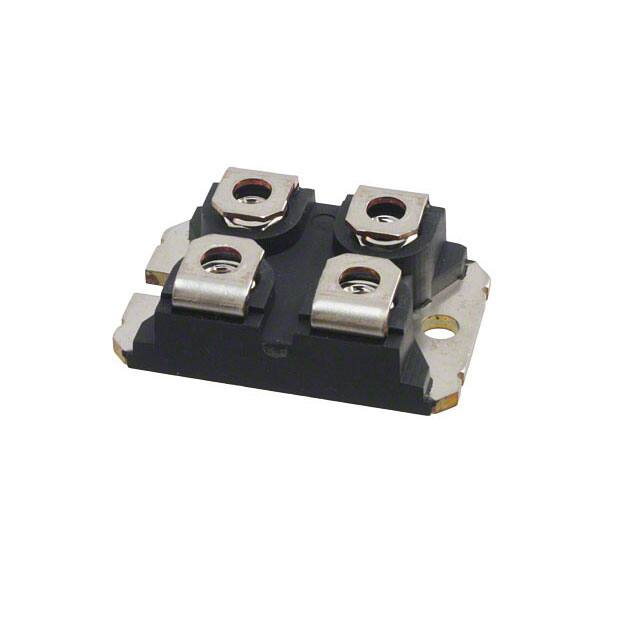
• Popular SOT-227 Package
ISOTOP ®
D
FREDFET
G
• Faster Switching
Unless stated otherwise, Microsemi discrete FREDFETs contain a single FREDFET die. This device is made with
two parallel FREDFET die. It is intended for switch-mode operation. It is not suitable for linear mode operation.
MAXIMUM RATINGS
Symbol
VDSS
ID
S
All Ratings: TC = 25°C unless otherwise specified.
Parameter
APT50M85JVFR
UNIT
500
Volts
Drain-Source Voltage
50
Continuous Drain Current @ TC = 25°C
1
Amps
IDM
Pulsed Drain Current
VGS
Gate-Source Voltage Continuous
±30
Gate-Source Voltage Transient
±40
Total Power Dissipation @ TC = 25°C
500
Watts
4
W/°C
VGSM
PD
TJ,TSTG
200
Linear Derating Factor
Lead Temperature: 0.063" from Case for 10 Sec.
IAR
Avalanche Current
EAR
Repetitive Avalanche Energy
EAS
-55 to 150
Operating and Storage Junction Temperature Range
TL
1
°C
300
30
(Repetitive and Non-Repetitive)
1
Single Pulse Avalanche Energy
Volts
Amps
30
4
mJ
1300
STATIC ELECTRICAL CHARACTERISTICS
BVDSS
ID(on)
RDS(on)
IDSS
IGSS
VGS(th)
Characteristic / Test Conditions
MIN
Drain-Source Breakdown Voltage (VGS = 0V, ID = 250µA)
500
Volts
50
Amps
On State Drain Current
2
(VDS > I D(on) x R DS(on) Max, VGS = 10V)
Drain-Source On-State Resistance
2
(VGS = 10V, 0.5 ID[Cont.])
TYP
MAX
0.085
Zero Gate Voltage Drain Current (VDS = VDSS, VGS = 0V)
500
UNIT
Ohms
µA
Zero Gate Voltage Drain Current (VDS = 0.8 VDSS, VGS = 0V, TC = 125°C)
2000
Gate-Source Leakage Current (VGS = ±30V, VDS = 0V)
±100
nA
4
Volts
Gate Threshold Voltage (VDS = VGS, ID = 1mA)
2
CAUTION: These Devices are Sensitive to Electrostatic Discharge. Proper Handling Procedures Should Be Followed.
Microsemi Website - http://www.microsemi.com
Downloaded from Elcodis.com electronic components distributor
050-5621 Rev A 6 - 2006
Symbol
�APT50M85JVFR
DYNAMIC CHARACTERISTICS
Symbol
Characteristic
Test Conditions
MIN
TYP
MAX
Ciss
Input Capacitance
VGS = 0V
9000
10800
Coss
Output Capacitance
VDS = 25V
1240
1740
Crss
Reverse Transfer Capacitance
f = 1 MHz
500
750
Qg
Total Gate Charge
VGS = 10V
390
535
Qgs
Gate-Source Charge
VDD = 0.5 VDSS
Qgd
Gate-Drain ("Miller ") Charge
ID = ID [Cont.] @ 25°C
42
170
65
255
VGS = 15V
15
30
t d(on)
3
Turn-on Delay Time
tr
Rise Time
t d(off)
Turn-off Delay Time
tf
VDD = 0.5 VDSS
17
34
ID = ID [Cont.] @ 25°C
52
80
RG = 0.6Ω
7
14
TYP
MAX
Fall Time
UNIT
pF
nC
ns
SOURCE-DRAIN DIODE RATINGS AND CHARACTERISTICS
Symbol
Characteristic / Test Conditions
IS
ISM
Pulsed Source Current
1
VSD
Diode Forward Voltage
2
dv/
MIN
50
Continuous Source Current (Body Diode)
Peak Diode Recovery
dt
200
(Body Diode)
(VGS = 0V, IS = -ID [Cont.])
dv/ 5
dt
UNIT
Amps
1.3
Volts
5
V/ns
t rr
Reverse Recovery Time
(IS = -ID [Cont.], di/dt = 100A/µs)
Tj = 25°C
300
Tj = 125°C
600
Q rr
Reverse Recovery Charge
(IS = -ID [Cont.], di/dt = 100A/µs)
Tj = 25°C
2.5
Tj = 125°C
8
IRRM
Peak Recovery Current
(IS = -ID [Cont.], di/dt = 100A/µs)
Tj = 25°C
16
Tj = 125°C
28
ns
µC
Amps
THERMAL / PACKAGE CHARACTERISTICS
Characteristic
Symbol
MIN
RθJC
Junction to Case
RθJA
Junction to Ambient
TYP
MAX
0.25
40
VIsolation
RMS Voltage (50-60 Hz Sinusoidal Waveform From Terminals to Mounting Base for 1 Min.)
Torque
Maximum Torque for Device Mounting Screws and Electrical Terminations.
1 Repetitive Rating: Pulse width limited by maximum junction
temperature.
2 Pulse Test: Pulse width < 380 µS, Duty Cycle < 2%
2500
13
D=0.5
0.1
0.2
0.05
0.1
0.05
Note:
PDM
Z JC, THERMAL IMPEDANCE (°C/W)
θ
050-5621 Rev A 6 - 2006
0.3
0.005
0.01
SINGLE PULSE
t1
t2
Duty Factor D = t1/t2
Peak TJ = PDM x ZθJC + TC
0.001
10-5
10-4
10-3
10-2
10-1
1.0
10
RECTANGULAR PULSE DURATION (SECONDS)
FIGURE 1, MAXIMUM EFFECTIVE TRANSIENT THERMAL IMPEDANCE, JUNCTION-TO-CASE vs PULSE DURATION
Downloaded from Elcodis.com electronic components distributor
lb•in
3 See MIL-STD-750 Method 3471
4 Starting T = +25°C, L = 2.89mH, R = 25Ω, Peak I = 30A
j
G
L
5 I - -I [Cont.], di/ = 100A/µs, V
S
D
DD - VDSS, Tj - 150°C, RG = 2.0Ω,
dt
VR = 200V
0.02
°C/W
Volts
Microsemi reserves the right to change, without notice, the specifications and information contained herein.
0.01
UNIT
�APT50M85JVFR
150
VGS=7V, 10V & 15V
120
6V
90
5.5V
60
5V
30
4.5V
ID, DRAIN CURRENT (AMPERES)
TJ = +25°C
120
TJ = +125°C
VDS> ID (ON) x RDS (ON)MAX.
250µSEC. PULSE TEST
@
很抱歉,暂时无法提供与“APT50M85JVFR”相匹配的价格&库存,您可以联系我们找货
免费人工找货- 国内价格 香港价格
- 20+413.0549420+53.38703