600V 8A
APT8DQ60K
APT8DQ60KG*
*G Denotes RoHS Compliant, Pb Free Terminal Finish.
ULTRAFAST SOFT RECOVERY RECTIFIER DIODE
(K)
PRODUCT APPLICATIONS
PRODUCT FEATURES
PRODUCT BENEFITS
• Anti-Parallel Diode
-Switchmode Power Supply
-Inverters
• Free Wheeling Diode
-Motor Controllers
-Converters
-Inverters
• Snubber Diode
• Ultrafast Recovery Times
• Low Losses
• Soft Recovery Characteristics
• Low Noise Switching
• PFC
• Cooler Operation
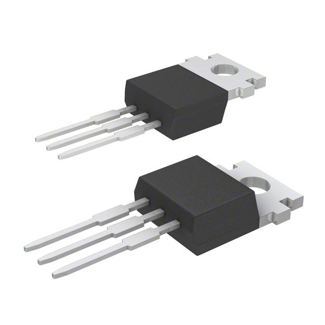
• Popular TO-220 Package or
Surface Mount D2 PAK Package
• Higher Reliability Systems
• Low Forward Voltage
• Low Leakage Current
• Avalanche Energy Rated
1
2
2
1
• Increased System Power
Density
1 - Cathode
2 - Anode
Back of Case - Cathode
MAXIMUM RATINGS
Symbol
VR
All Ratings: TC = 25°C unless otherwise specified.
Characteristic / Test Conditions
APT8DQ60K(G)
UNIT
600
Volts
Maximum D.C. Reverse Voltage
VRRM
Maximum Peak Repetitive Reverse Voltage
VRWM
Maximum Working Peak Reverse Voltage
IF(AV)
Maximum Average Forward Current (TC = 128°C, Duty Cycle = 0.5)
8
RMS Forward Current (Square wave, 50% duty)
16
IFSM
Non-Repetitive Forward Surge Current (TJ = 45°C, 8.3ms)
110
EAVL
Avalanche Energy (1A, 40mH)
20
IF(RMS)
TJ,TSTG
TL
Amps
-55 to 175
Operating and StorageTemperature Range
300
Lead Temperature for 10 Sec.
mJ
°C
STATIC ELECTRICAL CHARACTERISTICS
VF
Characteristic / Test Conditions
Forward Voltage
IRM
Maximum Reverse Leakage Current
CT
Junction Capacitance, VR = 200V
MIN
TYP
MAX
IF = 8A
2.0
2.4
IF = 16A
2.5
IF = 8A, TJ = 125°C
1.5
VR = 600V
25
VR = 600V, TJ = 125°C
500
Microsemi Website - http://www.microsemi.com
UNIT
Volts
16
µA
pF
053-4210 Rev K 6-2015
Symbol
�DYNAMIC CHARACTERISTICS
APT8DQ60K(G)
Characteristic
Symbol
Test Conditions
MIN
TYP
MAX
UNIT
trr
Reverse Recovery Time
IF = 1A, diF/dt = -100A/µs, VR = 30V, TJ = 25°C
-
14
trr
Reverse Recovery Time
-
19
Qrr
Reverse Recovery Charge
-
17
-
2
-
90
ns
-
160
nC
-
3
-
43
ns
-
250
nC
-
11
IRRM
IF = 8A, diF/dt = -200A/µs
VR = 400V, TC = 25°C
Maximum Reverse Recovery Current
trr
Reverse Recovery Time
Qrr
Reverse Recovery Charge
IRRM
IF = 8A, diF/dt = -200A/µs
Maximum Reverse Recovery Current
trr
Reverse Recovery Time
Qrr
Reverse Recovery Charge
IRRM
VR = 400V, TC = 125°C
IF = 8A, diF/dt = -1000A/µs
Maximum Reverse Recovery Current
VR = 400V, TC = 125°C
ns
nC
-
-
Amps
Amps
Amps
THERMAL AND MECHANICAL CHARACTERISTICS
Symbol
RθJC
WT
Characteristic / Test Conditions
MIN
Junction-to-Case Thermal Resistance
Package Weight
Torque
Maximum Mounting Torque
TYP
MAX
UNIT
2.7
°C/W
0.07
oz
1.9
g
10
lb•in
1.1
N•m
Microsemi reserves the right to change, without notice, the specifications and information contained herein.
D = 0.9
2.0
0.7
1.5
1.0
0.5
Note:
t1
0.3
0.1
0.05
Duty Factor D = 1 /t2
Peak T J = P DM x Z θJC + T C
t2
0.5
053-4210 Rev K 6-2015
2.5
P DM
Z JC, THERMAL IMPEDANCE (°C/W)
θ
3.0
0
10-5
SINGLE PULSE
10-4
t
10-3
10-2
10-1
1.0
RECTANGULAR PULSE DURATION (seconds)
FIGURE 1. MAXIMUM EFFECTIVE TRANSIENT THERMAL IMPEDANCE, JUNCTION-TO-CASE vs. PULSE DURATION
�TYPICAL PERFORMANCE CURVES
15
TJ = 125°C
10
TJ = 25°C
0
TJ = -55°C
Qrr, REVERSE RECOVERY CHARGE
(nC)
350
T = 125°C
J
V = 400V
R
16A
300
250
8A
200
150
4A
100
50
0
0
200 400 600 800 1000 1200
-diF /dt, CURRENT RATE OF CHANGE (A/µs)
Figure 4. Reverse Recovery Charge vs. Current Rate of Change
8A
4A
60
40
20
14
12
T = 125°C
J
V = 400V
16A
R
10
8
6
8A
4
4A
2
20
Duty cycle = 0.5
T = 175°C
18
trr
J
16
trr
IRRM
14
IF(AV) (A)
Kf, DYNAMIC PARAMETERS
(Normalized to X000A/µs)
80
0
200 400 600 800 1000 1200
-diF /dt, CURRENT RATE OF CHANGE (A/µs)
Figure 5. Reverse Recovery Current vs. Current Rate of Change
0.6
12
10
8
0.4
6
Qrr
4
0.2
2
0.0
25
50
75
100 125 150
TJ, JUNCTION TEMPERATURE (°C)
Figure 6. Dynamic Parameters vs. Junction Temperature
0
0
25
50
75
100 125 150 175
Case Temperature (°C)
Figure 7. Maximum Average Forward Current vs. CaseTemperature
50
20
10
0
1
10
100 200
VR, REVERSE VOLTAGE (V)
Figure 8. Junction Capacitance vs. Reverse Voltage
053-4210 Rev K 6-2015
30
40
CJ, JUNCTION CAPACITANCE
(pF)
60
0.8
16A
0
Qrr
1.0
R
100
0
200 400 600
800 1000 1200
-diF /dt, CURRENT RATE OF CHANGE(A/µs)
Figure 3. Reverse Recovery Time vs. Current Rate of Change
IRRM, REVERSE RECOVERY CURRENT
(A)
0.5 1.0 1.5 2.0 2.5 3.0 3.5
VF, ANODE-TO-CATHODE VOLTAGE (V)
Figure 2. Forward Current vs. Forward Voltage
400
APT8DQ60K(G)
T = 125°C
J
V = 400V
0
0
1.2
trr, REVERSE RECOVERY TIME
(ns)
TJ = 175°C
20
25
5
120
IF, FORWARD CURRENT
(A)
30
�APT8DQ60K(G)
Vr
APT6038BLL
diF /dt Adjus t
+18V
0V
D.U.T.
30µH
trr/Q rr
Waveform
PEARSON 2878
CURRENT
TRANSFORMER
Figure 9. Diode Test Circuit
1 IF - Forward Conduction Current
2 diF/dt - Rate of Diode Current Change Through Zero Crossing.
3 IRRM - Maximum Reverse Recovery Current
1
Zer o
4 trr - Reverse Recovery Time measured from zero crossing where
diode current goes from positive to negative, to the point at
which the straight line through IRRM and 0.25, IRRM passes through zero.
5 Qrr - Area Under the Curve Defined by IRRM and tRR.
Figure 10. Diode Reverse Recovery Waveform Definition
TO-220 (K) Package Outline
e3 100% Sn
Cathode
Cathode
053-4210 Rev K 6-2015
4
Anode
Dimensions in millimeters and [inches]
5
3
2
0.25 I RRM
�TYPICAL PERFORMANCE CURVES
APT8DQ60K(G)
Disclaimer:
Microsemi reserves the right to change the configuration, functionality and performance of its products at anytime without any notice. This
product has been subject to limited testing and should not be used in conjunction with life-support or other mission-critical equipment or
applications. Microsemi assumes no liability whatsoever, and Microsemi disclaims any express or implied warranty, relating to sale and/or
use of Microsemi products including liability or warranties relating to fitness for a particular purpose, merchantability, or infringement of any
patent, copyright or other intellectual property right. Any performance specifications believed to be reliable but are not verified and customer or
user must conduct and complete all performance and other testing of this product as well as any user or customer's final application. User or
customer shall not rely on any data and performance specifications or parameters provided by Microsemi. It is the customer’s and user’s responsibility to independently determine suitability of any Microsemi product and to test and verify the same. The information contained herein
is provided “AS IS, WHERE IS” and with all faults, and the entire risk associated with such information is entirely with the User. Microsemi
specifically disclaims any liability of any kind including for consequential, incidental and punitive damages as well as lost profit. The product is
subject to other terms and conditions which can be located on the web at http://www.microsemi.com/terms-a-conditions.
053-4210 Rev K 6-2015
The information contained in the document (unless it is publicly available on the Web without access restrictions) is PROPRIETARY AND
CONFIDENTIAL information of Microsemi and cannot be copied, published, uploaded, posted, transmitted, distributed or disclosed or used
without the express duly signed written consent of Microsemi. If the recipient of this document has entered into a disclosure agreement with
Microsemi, then the terms of such Agreement will also apply. This document and the information contained herein may not be modified, by
any person other than authorized personnel of Microsemi. No license under any patent, copyright, trade secret or other intellectual property
right is granted to or conferred upon you by disclosure or delivery of the information, either expressly, by implication, inducement, estoppels or
otherwise. Any license under such intellectual property rights must be approved by Microsemi in writing signed by an officer of Microsemi.
�