ATWINC3400A-MU
ATWINC3400A-MU IEEE® 802.11 b/g/n Network Controller
with Integrated Bluetooth® SoC
Introduction
The Microchip ATWINC3400 is an IEEE 802.11 b/g/n RF/Baseband/Medium Access Control (MAC) network controller
with Bluetooth Low Energy. It is Bluetooth 5.0 certified and optimized for low-power and high-performance
applications. The ATWINC3400 radio features fully integrated Power Amplifier (PA), Low Noise Amplifier (LNA),
Switch, Power Management Unit (PMU) and integrated Flash memory for system software. The ATWINC3400 offers
high integration and minimal bill of materials thereby reducing system cost. The ATWINC3400 external clock sources
needed are a high-speed crystal or oscillator with 26 MHz, and a 32.768 kHz clock for sleep operation. The
ATWINC3400 is available in small, 6*6mm QFN packaging.
The ATWINC3400 utilizes highly optimized IEEE 802.11 and Bluetooth coexistence protocols, and provides a Serial
Peripheral Interface (SPI) to interface with the host controller.
Features
®
Wi-Fi Features:
•
•
•
•
•
•
•
•
•
•
•
•
•
•
•
IEEE 802.11 b/g/n with Single Spatial Stream (1x1), 2.4 GHz ISM Band
Integrated PA and T/R Switch
Superior Sensitivity and Range via Advanced PHY Signal Processing
Advanced Equalization and Channel Estimation
Advanced Carrier and Timing Synchronization
Supports Soft-AP
Supports IEEE 802.11 WEP, WPA, and WPA2 Personal and WPA2 Enterprise (firmware v. 1.3.1 or later)
Superior MAC Throughput through Hardware Accelerated Two-Level A-MSDU/A-MPDU Frame Aggregation and
Block Acknowledgment
On-Chip Memory Management Engine to Reduce the Host Load
Operating Temperature Range from -40°C to +85°C
SPI Host Interface
Integrated Flash Memory for Wi-Fi and Bluetooth System Software
Low Leakage On-Chip Memory for State Variables
Fast AP Re-Association (150 ms)
On-Chip Network Stack to Offload Host MCU
– Network Features: TCP, UDP, DHCP, ARP, HTTP, TLS, DNS, and SNTP
Bluetooth Features:
•
•
•
Bluetooth Low Energy 5.0
Adaptive Frequency Hopping (AFH)
Superior Sensitivity and Range
© 2020 Microchip Technology Inc.
Datasheet
DS70005390A-page 1
�ATWINC3400A-MU
Table of Contents
Introduction.....................................................................................................................................................1
Features......................................................................................................................................................... 1
1.
Ordering Information and IC Marking......................................................................................................4
2.
Functional Overview................................................................................................................................5
2.1.
2.2.
2.3.
2.4.
3.
Clocking................................................................................................................................................ 10
3.1.
3.2.
4.
Crystal Oscillator........................................................................................................................ 10
Low-Power Oscillator..................................................................................................................11
CPU and Memory Subsystem...............................................................................................................12
4.1.
4.2.
4.3.
5.
Block Diagram.............................................................................................................................. 5
Pinout Information........................................................................................................................ 6
Pinout Description........................................................................................................................ 6
Package Description.................................................................................................................... 9
Processor................................................................................................................................... 12
Memory Subsystem....................................................................................................................12
Nonvolatile Memory (eFuse)...................................................................................................... 12
WLAN Subsystem................................................................................................................................. 14
5.1.
5.2.
MAC........................................................................................................................................... 14
5.1.1.
Features.......................................................................................................................14
PHY............................................................................................................................................ 15
5.2.1.
Features.......................................................................................................................15
6.
Bluetooth Low Energy........................................................................................................................... 16
7.
Radio.....................................................................................................................................................17
7.1.
7.2.
7.3.
7.4.
8.
External Interfaces................................................................................................................................ 21
8.1.
8.2.
8.3.
8.4.
9.
WLAN Transmitter Performance................................................................................................ 17
WLAN Receiver Performance.................................................................................................... 18
Bluetooth Transmitter Performance............................................................................................19
Bluetooth Receiver Performance............................................................................................... 20
Interfacing with the Host Microcontroller.................................................................................... 21
I2C Slave Interface..................................................................................................................... 22
8.2.1.
I2C Slave Timing.......................................................................................................... 22
SPI Slave Interface.....................................................................................................................23
8.3.1.
Overview......................................................................................................................23
8.3.2.
SPI Timing................................................................................................................... 23
UART Interface...........................................................................................................................25
Power Management.............................................................................................................................. 26
9.1.
9.2.
Power Architecture..................................................................................................................... 26
Power Consumption................................................................................................................... 27
9.2.1.
Description of Device States........................................................................................27
© 2020 Microchip Technology Inc.
Datasheet
DS70005390A-page 2
�ATWINC3400A-MU
9.2.2.
9.2.3.
9.2.4.
9.2.5.
Controlling Device States............................................................................................ 27
Restrictions for Power States...................................................................................... 28
Power-Up/Down Sequence......................................................................................... 28
Digital I/O Pin Behavior During Power-Up Sequences................................................ 29
10. Electrical Characteristics.......................................................................................................................30
10.1. Absolute Maximum Ratings........................................................................................................30
10.2. Recommended Operating Conditions........................................................................................ 30
10.3. DC Characteristics..................................................................................................................... 31
11. Package Outline Drawing......................................................................................................................32
12. Reference Design................................................................................................................................. 33
13. Design Considerations.......................................................................................................................... 36
13.1. Placement and Routing Guidelines............................................................................................ 36
13.1.1. Power and Ground.......................................................................................................36
13.1.2. RF Traces and Components........................................................................................36
13.1.3. Power Management Unit............................................................................................. 37
13.1.4. Ground.........................................................................................................................38
13.2. Sensitive Traces.........................................................................................................................39
13.2.1. Signals......................................................................................................................... 39
13.2.2. Supplies....................................................................................................................... 39
13.3. Additional Suggestions...............................................................................................................39
13.4. Interferers................................................................................................................................... 40
13.5. Antenna...................................................................................................................................... 40
13.6. Reflow Profile Information.......................................................................................................... 40
14. Reference Documentation.................................................................................................................... 41
15. Document Revision History...................................................................................................................42
The Microchip Website.................................................................................................................................43
Product Change Notification Service............................................................................................................43
Customer Support........................................................................................................................................ 43
Microchip Devices Code Protection Feature................................................................................................ 43
Legal Notice................................................................................................................................................. 43
Trademarks.................................................................................................................................................. 44
Quality Management System....................................................................................................................... 44
Worldwide Sales and Service.......................................................................................................................45
© 2020 Microchip Technology Inc.
Datasheet
DS70005390A-page 3
�ATWINC3400A-MU
Ordering Information and IC Marking
1.
Ordering Information and IC Marking
The following table provides the ordering details for the ATWINC3400.
Table 1-1. Ordering Details
Ordering Code
ATWINC3400A-MU-ABCD
Package Type
QFN in Tray, Tape
and Reel
Package Size
6 mm x 6 mm
IC Marking
ATWINC3400A
Note:
1. ABCD interprets as:
"A" can be "Y" indicating Tray or "T" indicating Tape and Reel.
"BCD" equals to "042" for part assigned with a MAC ID and blank for part with no MAC ID.
The following table lists the possible combinations for ordering the ATWINC3400A.
Table 1-2.
Ordering Code
Description
ATWINC3400A-MU-T
No MAC ID and ship in Tape and Reel
ATWINC3400A-MU-T042
MAC ID assigned and ship in Tape and Reel
ATWINC3400A-MU-Y
No MAC ID and ship in Tray
ATWINC3400A-MU-Y042
MAC ID assigned and ship in Tray
© 2020 Microchip Technology Inc.
Datasheet
DS70005390A-page 4
�ATWINC3400A-MU
Functional Overview
2.
Functional Overview
2.1
Block Diagram
The ATWINC3400 block diagram is shown in the following figure.
Figure 2-1. ATWINC3400 Block Diagram
© 2020 Microchip Technology Inc.
Datasheet
DS70005390A-page 5
�ATWINC3400A-MU
Functional Overview
2.2
Pinout Information
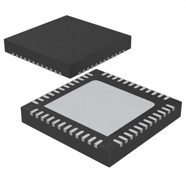
ATWINC3400 is offered in an exposed pad 48-pin QFN package. This package has an exposed paddle that must be
connected to the system board ground. The QFN package pin assignment is shown in following figure.
48 47 46 45 44 43 42
VDDRF_RX
1
VDD_AMS
2
GPIO_18
GPIO_19
GPIO_20
IRQN
I2C_SCL_M
I2C_SDA_M
XO_N
XO_P
VDD_SXDIG
VDD_VCO
VDDIO_A
TP_P
Figure 2-2. ATWINC3400 Pin Assignment
41 40 39 38 37
36 GPIO_17
35 GPIO_7
49 Paddle VSS
VDDRF_TX
3
VDD_BATT
4
33 VDDIO_1
RFIOP
5
32 SPI_SSN
RFION
6
TEST_MODE
7
SPI_CFG
8
29 GPIO_8
N/C
9
28 RTC
34 SPI_MOSI
31 SPI_MISO
ATWINC3400
30 SPI_SCK
N/C 10
27 CHIP_EN
N/C 11
26 VREG_BUCK
25 VSW
2.3
VBATT_BUCK
UART_RXD
UART_TXD
GPIO_4
GPIO_3
VDDIO_0
VDDC
I2C_SCL_S
I2C_SDA_S
BT_RXD
21 22 23 24
BT_TXD
13 14 15 16 17 18 19 20
RESETN
N/C 12
Pinout Description
The ATWINC3400 pins with default peripheral mapping are described in the following table.
Table 2-1. ATWINC3400 Pin Description
Pin Number Pin Name
Pin Type
Description
1
VDDRF_RX
Power
Tuner RF RX Supply
2
VDD_AMS
Power
Tuner BB Supply
3
VDDRF_TX
Power
Tuner RF TX Supply
4
VDD_BATT
Power
Battery Supply for PA
5
RFIOP
Analog
Wi-Fi/BLE Pos RF Differential I/O
6
RFION
Analog
Wi-Fi/BLE Neg RF Differential I/O
© 2020 Microchip Technology Inc.
Datasheet
DS70005390A-page 6
�ATWINC3400A-MU
Functional Overview
...........continued
Pin Number Pin Name
Pin Type
Description
7
TEST_MODE
Digital Input
Test Mode – Tie to GND
8
SPI_CFG
Digital Input
Tie to VDDIO through 1 MΩ resistor for
selecting SPI interface
9
N/C
-
Not Connected
10
N/C
-
Not Connected
11
N/C
-
Not Connected
12
N/C
-
Not Connected
13
RESETN
Digital Input
•
•
•
14
BT_TXD
Digital I/O, Programmable Pull-Up
•
•
•
15
BT_RXD
Digital I/O, Programmable Pull-Up
•
•
•
Active-Low Hard Reset pin
When the Reset pin is asserted
low, the module is in the Reset
state. When the Reset pin is
asserted high, the module
functions normally
This pin must connect to a host
output that is low by default on
power-up. If the host output is tristated, add a 1 MΩ pull down
resistor to ensure a low level at
power-up
Bluetooth UART Transmit Data
Output pin
Used only during debug for DTM
interface. SPI is the data and
control interface with host
microcontroller
It is recommended to add a test
point for this pin
Bluetooth UART Receive Data
Input pin
Used only during debug for DTM
interface. SPI is the data and
control interface with host
microcontroller
It is recommended to add a test
point for this pin
16
I2C_SDA_S
Digital I/O, Programmable Pull-Up
•
•
I2C Slave Data pin
Used only for test purposes. It is
recommended to add a test point
for this pin
17
I2C_SCL_S
Digital I/O, Programmable Pull-Up
•
•
I2C Slave Clock pin
Used only for test purposes. It is
recommended to add a test point
for this pin
18
VDDC
Power
Digital Core Power Supply
19
VDDIO_0
Power
Digital I/O Power Supply
© 2020 Microchip Technology Inc.
Datasheet
DS70005390A-page 7
�ATWINC3400A-MU
Functional Overview
...........continued
Pin Number Pin Name
Pin Type
Description
20
GPIO_3
Digital I/O, Programmable Pull-Up
GPIO_3(1)
21
GPIO_4
Digital I/O, Programmable Pull-Up
GPIO_4(1)
22
UART_TXD
Digital I/O, Programmable Pull-Up
•
•
Wi-Fi UART TXD Output pin
Used only for debug development
purposes. It is recommended to
add a test point for this pin
23
UART_RXD
Digital I/O, Programmable Pull-Up
•
•
Wi-Fi UART RXD Input pin
Used only for debug development
purposes. It is recommended to
add a test point for this pin
24
VBATT_BUCK
Power
Battery Supply for DC Converter
25
VSW
Power
Switching Output of DC Converter
26
VREG_BUCK
Power
Core Power from DC Converter
27
CHIP_EN
Analog
•
•
•
PMU Enable pin
When the CHIP_EN pin is
asserted high, the module is
enbled. When the CHIP_EN pin is
asserted low, the module is
disabled or put into Power-Down
mode
Connect to a host output that is
low by default at power-up. If the
host output is tri-stated, add a 1
MΩ pull down resistor if
necessary to ensure a low level at
power-up
28
RTC
Digital I/O, Programmable Pull-Up
29
GPIO8
Digital I/O, Programmable Pull-Up
GPIO_8(1)
30
SPI_SCK
Digital I/O, Programmable Pull-Up
SPI Clock
31
SPI_MISO
Digital I/O, Programmable Pull-Up
SPI MISO (Master In Slave Output) pin
32
SPI_SSN
Digital I/O, Programmable Pull-Up
SPI Slave Select
33
VDDIO_1
Power
Digital I/O Power Supply
34
SPI_MOSI
Digital I/O, Programmable Pull-Up
SPI MOSI (Multiple Output Slave
Input) pin
35
GPIO7
Digital I/O, Programmable Pull-Up
GPIO_7(1)
36
GPIO_17
Digital I/O, Programmable Pull-Down
GPIO_17(1)
37
GPIO_18
Digital I/O, Programmable Pull-Down
GPIO_18(1)
38
GPIO_19
Digital I/O, Programmable Pull-Down
GPIO_19(1)
39
GPIO_20
Digital I/O, Programmable Pull-Down
GPIO_20(1)
© 2020 Microchip Technology Inc.
Datasheet
•
•
RTC Clock Input pin
This pin must connect to a 32.768
kHz clock source.
DS70005390A-page 8
�ATWINC3400A-MU
Functional Overview
...........continued
Pin Number Pin Name
Pin Type
40
Digital I/O, Programmable Pull-Up
IRQN
Description
•
•
ATWINC3400A Module Host
Interrupt Request Output pin
This pin must connect to a host
interrupt pin
41
I2C_SCL_M
Digital I/O, Programmable Pull-Up
I2C Mater Clock Pin
42
I2C_SDA_M
Digital I/O, Programmable Pull-Up
I2C Master Data Pin
43
XO_N
Analog
Crystal Oscillator N
44
XO_P
Analog
Crystal Oscillator P
45
VDD_SXDIG
Power
SX Power Supply
46
VDD_VCO
Power
VCO Power Supply
47
VDDIO_A
Power
Tuner VDDIO Power Supply
48
TP_P
Analog
Test Pin, leave unconnected
49
PADDLE VSS
Power
Connect to System Board Ground
Note:
1. Usage of the GPIO functionality is not supported by the FW. The data sheet is updated once support for this
feature is added.
2.4
Package Description
The following table provides the physical details of ATWINC3400 devices.
Table 2-2. ATWINC3400 QFN Package Information
Parameter
Value
Units
Tolerance
Package Size
6x6
mm
±0.1 mm
QFN Pad Count
48
-
-
Total Thickness
0.85
mm
+0.15 mm/-0.05 mm
QFN Pad Pitch
0.40
mm
-
Pad Width
0.20
mm
±0.05 mm
Exposed Pad size
4.7 x 4.7
mm
-
For drawing details, refer to 11. Package Outline Drawing
© 2020 Microchip Technology Inc.
Datasheet
DS70005390A-page 9
�ATWINC3400A-MU
Clocking
3.
Clocking
This section details the clocking sources of the ATWINC3400.
3.1
Crystal Oscillator
The following table provides the values of the ATWINC3400 crystal oscillator parameters.
Table 3-1. Crystal Oscillator Parameters
Parameter
Min.
Typ.
Max.
Unit
Crystal Resonant Frequency
-
26
-
MHz
Crystal Equivalent Series
Resistance
-
50
-
Ohm
Stability - Initial Offset1
-100
-
100
ppm
Stability - Temperature and
Aging
-25
-
25
ppm
Note: 1. Initial Offset must be calibrated to maintain ±25 ppm in all operating conditions. This calibration is
performed during final production testing.
The block diagram in the following figure (a) shows how the internal Crystal Oscillator (XO) is connected to the
external crystal. The XO has 5 pF internal capacitance on each terminal XO_P and XO_N. To bypass the crystal
oscillator with an external reference, an external signal capable of driving 5 pF can be applied to the XO_N terminal
as shown in figure (b).
The XO has 5 pF internal capacitance on each terminal XO_P and XO_N. This internal capacitance must be
considered when calculating the external loading capacitance, c_onboard, for the XTAL.
Figure 3-1. ATWINC3400 XO Connections
External Clock
C_onboard
XTAL
XO_N
C_onboard
XO_P
C_onchip
XO_N
XO_P
C_onchip
C_onchip
(a)
C_onchip
(b)
(a) Crystal Oscillator is Used
(b) Crystal Oscillator is Bypassed
The following table specifies the electrical and performance requirements for the external clock.
© 2020 Microchip Technology Inc.
Datasheet
DS70005390A-page 10
�ATWINC3400A-MU
Clocking
Table 3-2. Bypass Clock Specification
3.2
Parameter
Min.
Typ.
Max.
Unit
Comments
Oscillator
frequency
-
26
-
MHz
Must drive 5 pF
load at desired
frequency
Voltage swing
0.5
-
1.2
VPP
Must be AC
coupled
Stability Temperature and
Aging
-25
-
+25
ppm
-
Phase Noise
-
-
-130
dBc/Hz
At 10 kHz offset
Jitter (RMS)
-
-


 工商网监
湘ICP备2023018690号
工商网监
湘ICP备2023018690号
