1N5711UR-1, 1N5712UR-1, 1N6857UR-1,
and 1N6858UR-1 plus CDLL equivalents
Qualified Levels:
JAN, JANTX, and
JANTXV
Schottky Barrier Diode
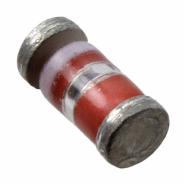
MELF Surface Mount
Available on
commercial
versions
Qualified per MIL-PRF-19500/444
DESCRIPTION
This Schottky barrier diode is metallurgically bonded and offers military grade qualifications
for high-reliability applications. This small diode is hermetically sealed and bonded into a
DO-213AA glass package. Also included in this datasheet are Microsemi’s CDLL numbered
variants of this series (military qualification grades not are not available for the CDLL prefix
part numbers).
DO-213AA (MELF)
Package
Important: For the latest information, visit our website http://www.microsemi.com.
FEATURES
•
Surface mount equivalent of JEDEC registered 1N5711, 1N5712, 1N6857, and 1N6858 numbers.
•
Hermetically sealed glass construction.
•
Metallurgically bonded.
•
Double plug construction.
•
JAN, JANTX, JANTXV and commercial qualifications also available per MIL-PRF-19500/444 on
“1N” numbers only.
UB package
(3-pin surface mount)
1N5711UB, 1N5712UB
(B, CC, CA)
(See Part Nomenclature for all available options).
•
Also available in:
RoHS compliant versions available (commercial grade only).
DO-35 package
(axial-leaded)
1N5711-1, 1N5712-1,
1N6857-1, and 1N6858-1
APPLICATIONS / BENEFITS
•
•
•
Low reverse leakage characteristics.
Small size for high density mounting using the surface mount method (see package illustration).
ESD sensitive to Class 1.
MAXIMUM RATINGS @ 25 ºC unless otherwise stated
Parameters/Test Conditions
Junction and Storage Temperature
Thermal Resistance, Junction-to-End Cap
Average Rectified Output Current:
(1)
5711 & 6263 types
(2)
2810, 5712 & 6858 types
(3)
6857 types
Solder Temperature @ 10 s
Symbol
TJ and TSTG
R ӨJEC
Value
-65 to +150
250
Unit
ºC
ºC/W
IO
33
75
150
260
mA
NOTES: 1. At T EC and T SP = +140 °C, derate I O to 0 at +150 °C.
2. At T EC and T SP = +130 °C, derate I O to 0 at +150 °C.
3. At T EC and T SP = +110°C, derate I O to 0 at +150 °C.
o
MSC – Lawrence
6 Lake Street,
Lawrence, MA 01841
Tel: 1-800-446-1158 or
(978) 620-2600
Fax: (978) 689-0803
C
MSC – Ireland
Gort Road Business Park,
Ennis, Co. Clare, Ireland
Tel: +353 (0) 65 6840044
Fax: +353 (0) 65 6822298
Website:
www.microsemi.com
T4-LDS-0040-1, Rev. 1 (6/4/13)
©2013 Microsemi Corporation
Page 1 of 7
�1N5711UR-1, 1N5712UR-1, 1N6857UR-1,
and 1N6858UR-1 plus CDLL equivalents
MECHANICAL and PACKAGING
•
•
•
•
•
•
•
•
CASE: Hermetically sealed glass DO-213AA MELF (SOD-80, LL34) case package.
TERMINALS: Tin/lead plated or RoHS compliant matte-tin (on commercial grade only) over copper clad steel. Solderable per
MIL-STD-750, method 2026.
POLARITY: Cathode end is banded.
MOUNTING: The axial coefficient of expansion (COE) of this device is approximately +6PPM/°C. The COE of the mounting
surface system should be selected to provide a suitable match with this device.
MARKING: Part number.
TAPE & REEL option: Standard per EIA-296. Consult factory for quantities.
WEIGHT: Approximately 0.2 grams.
See Package Dimensions on last page.
PART NOMENCLATURE
JAN
1N5711
UR -1 (e3)
Reliability Level
JAN = JAN level
JANTX = JANTX level
JANTXV = JANTXV level
Blank = Commercial grade
RoHS Compliance
e3 = RoHS compliant (on
commercial grade only)
Blank = non-RoHS compliant
Metallurgically Bonded
JEDEC type number
(see Electrical Characteristics
table)
MELF Surface Mount
CDLL
2810
(e3)
Microsemi Designation
RoHS Compliance
e3 = RoHS compliant
Blank = non-RoHS compliant
Series number
(see Electrical Characteristics
table)
SYMBOLS & DEFINITIONS
Definition
Symbol
C
f
IR
IO
t rr
V (BR)
Capacitance: The capacitance in pF at a frequency of 1 MHz and specified voltage.
frequency
Reverse Current: The dc current flowing from the external circuit into the cathode terminal at the specified voltage V R.
Average Rectified Output Current: The Output Current averaged over a full cycle with a 50 Hz or 60 Hz sine-wave
input and a 180 degree conduction angle.
Reverse Recovery Time: The time interval between the instant the current passes through zero when changing from
the forward direction to the reverse direction and a specified decay point after a peak reverse current occurs.
Breakdown Voltage: A voltage in the breakdown region.
VF
Forward Voltage: A positive dc anode-cathode voltage the device will exhibit at a specified forward current.
VR
Reverse Voltage: A positive dc cathode-anode voltage below the breakdown region.
Working Peak Reverse Voltage: The peak voltage excluding all transient voltages (ref JESD282-B). Also sometimes
known historically as PIV.
V RWM
T4-LDS-0040-1, Rev. 1 (6/4/13)
©2013 Microsemi Corporation
Page 2 of 7
�1N5711UR-1, 1N5712UR-1, 1N6857UR-1,
and 1N6858UR-1 plus CDLL equivalents
ELECTRICAL CHARACTERISTICS @ T A = 25 ºC unless otherwise noted
TYPE
NUMBER
1N5711UR-1
1N5712UR-1
1N6857UR-1
1N6858UR-1
CDLL2810
CDLL5711
CDLL5712
CDLL6263
CDLL6857
CDLL6858
MINIMUM
BREAKDOWN
VOLTAGE
MAXIMUM
FORWARD
VOLTAGE
MAXIMUM
FORWARD
VOLTAGE
WORKING
PEAK
REVERSE
VOLTAGE
V (BR) @ 10 µA
Volts
70
20
20
70
20
70
20
60
20
70
V F @ 1 mA
Volts
0.41
0.41
0.35
0.36
0.41
0.41
0.41
0.41
0.35
0.36
VF @ IF
V @ mA
1.0 @ 15
1.0 @ 35
0.75 @ 35
0.65 @ 15
1.0 @ 35
1.0 @ 15
1.0 @ 35
1.0 @ 15
0.75 @ 35
0.65 @ 15
V RWM
V (pk)
50
16
16
50
50
50
16
16
16
50
MAXIMUM
REVERSE
LEAKAGE
CURRENT
nA
200
150
150
200
100
200
150
200
150
200
IR @ VR
Volts
50
16
16
50
15
50
16
50
16
50
MAXIMUM
CAPACITANCE
@ VR = 0
VOLTS
f = 1.0 MHz
CT
pF
2.0
2.0
4.5
4.5
2.0
2.0
2.0
2.2
4.5
4.5
NOTE:
1. Effective minority carrier lifetime (τ) is 100 pico seconds.
T4-LDS-0040-1, Rev. 1 (6/4/13)
©2013 Microsemi Corporation
Page 3 of 7
�1N5711UR-1, 1N5712UR-1, 1N6857UR-1,
and 1N6858UR-1 plus CDLL equivalents
IF – Forward Current (mA)
GRAPHS
V F – Forward Voltage (V)
IR – Reverse Current (nA)
FIGURE 1
I-V Curve showing typical Forward Voltage Variation
Temperature for the 1N5712UR-1, CDLL5712 and CDLL2810 Schottky Diodes
V R – Reverse Voltage (V) (PULSED)
FIGURE 2
1N5712UR-1, CDLL5712 and CDLL2810 Typical variation of Reverse
Current (I R ) vs Reverse Voltage (V R ) at Various Temperatures
T4-LDS-0040-1, Rev. 1 (6/4/13)
©2013 Microsemi Corporation
Page 4 of 7
�1N5711UR-1, 1N5712UR-1, 1N6857UR-1,
and 1N6858UR-1 plus CDLL equivalents
IF – Forward Current (mA)
GRAPHS
V F – Forward Voltage (V)
IR – Reverse Current (nA)
FIGURE 3
I – V curve showing typical Forward Voltage Variation
With Temperature Schottky Diode 1N5711UR-1
V R – Reverse Voltage (V) (PULSED)
FIGURE 4
1N5711UR-1 Typical Variation of Reverse Current (I R ) vs Reverse Voltage (V R )
at Various Temperatures
T4-LDS-0040-1, Rev. 1 (6/4/13)
©2013 Microsemi Corporation
Page 5 of 7
�1N5711UR-1, 1N5712UR-1, 1N6857UR-1,
and 1N6858UR-1 plus CDLL equivalents
RD – Dynamic Resistance (Ohms)
GRAPHS
I F – Forward Current (mA) (PULSED)
FIGURE 5
Typical Dynamic Resistance (R D ) vs Forward Current (I F )
T4-LDS-0040-1, Rev. 1 (6/4/13)
©2013 Microsemi Corporation
Page 6 of 7
�1N5711UR-1, 1N5712UR-1, 1N6857UR-1,
and 1N6858UR-1 plus CDLL equivalents
PACKAGE DIMENSIONS
DIM
BD
BL
ECT
S
INCH
MIN
MAX
0.063 0.067
0.130 0.146
0.016 0.022
0.001 min
MILLIMETERS
MIN
MAX
1.60
1.70
3.30
3.71
0.41
0.56
0.03 min
NOTES:
1. Dimensions are in inches. Millimeters are given for information only.
2. Dimensions are pre-solder dip.
3. Referencing to dimension S, minimum clearance of glass body to mounting surface on all orientations.
4. In accordance with ASME Y14.5M, diameters are equivalent to Φx symbology.
PAD LAYOUT
A
B
C
T4-LDS-0040-1, Rev. 1 (6/4/13)
©2013 Microsemi Corporation
INCH
0.200
0.055
0.080
mm
5.08
1.40
2.03
Page 7 of 7
�


 工商网监
湘ICP备2023018690号
工商网监
湘ICP备2023018690号
