MCP2515
Stand-Alone CAN Controller with SPI Interface
Features:
Description
• Implements CAN V2.0B at 1 Mb/s:
- 0 – 8 byte length in the data field
- Standard and extended data and remote
frames
• Receive Buffers, Masks and Filters:
- Two receive buffers with prioritized message
storage
- Six 29-bit filters
- Two 29-bit masks
• Data Byte Filtering on the First Two Data Bytes
(applies to standard data frames)
• Three Transmit Buffers with Prioritization and
Abort Features
• High-Speed SPI Interface (10 MHz):
- SPI modes 0,0 and 1,1
• One-Shot mode Ensures Message Transmission
is Attempted Only One Time
• Clock Out Pin with Programmable Prescaler:
- Can be used as a clock source for other
device(s)
• Start-of-Frame (SOF) Signal is Available for
Monitoring the SOF Signal:
- Can be used for time-slot-based protocols
and/or bus diagnostics to detect early bus
degradation
• Interrupt Output Pin with Selectable Enables
• Buffer Full Output Pins Configurable as:
- Interrupt output for each receive buffer
- General purpose output
• Request-to-Send (RTS) Input Pins Individually
Configurable as:
- Control pins to request transmission for each
transmit buffer
- General purpose inputs
• Low-Power CMOS Technology:
- Operates from 2.7V – 5.5V
- 5 mA active current (typical)
- 1 µA standby current (typical) (Sleep mode)
• Temperature Ranges Supported:
- Industrial (I): -40°C to +85°C
- Extended (E): -40°C to +125°C
Microchip Technology’s MCP2515 is a stand-alone
Controller Area Network (CAN) controller that
implements the CAN specification, version 2.0B. It is
capable of transmitting and receiving both standard
and extended data and remote frames. The MCP2515
has two acceptance masks and six acceptance filters
that are used to filter out unwanted messages, thereby
reducing the host MCU’s overhead. The MCP2515
interfaces with microcontrollers (MCUs) via an industry
standard Serial Peripheral Interface (SPI).
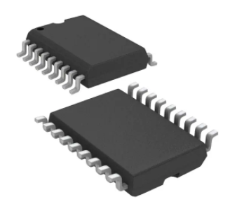
Package Types
18-Lead PDIP/SOIC
1
18
VDD
RXCAN
2
17
RESET
CLKOUT/SOF
3
16
CS
TX0RTS
4
15
SO
TX1RTS
5
14
SI
TX2RTS
6
13
SCK
OSC2
7
12
INT
OSC1
8
11
RX0BF
9
10
RX1BF
1
2
3
4
5
6
7
8
9
10
20
19
18
17
16
15
14
13
12
11
VDD
RESET
CS
SO
SI
NC
SCK
INT
RX0BF
RX1BF
Vss
CS
MCP2515
RESET
VDD
MCP2515
20-Lead 4x4 QFN*
RXCAN
TXCAN
RXCAN
CLKOUT/SOF
TX0RTS
TX1RTS
NC
TX2RTS
OSC2
OSC1
VSS
TXCAN
20-LEAD TSSOP
20 19 18 17 16
15 SO
CLKOUT 1
TX0RTS 2
14 SI
EP
21
TX1RTS 3
NC 4
13 NC
12 SCK
11 INT
8
OSC1
GND
9 10
RX0BF
7
RX1BF
6
OSC2
TX2RTS 5
* Includes Exposed Thermal
Pad (EP); see Table 1-1.
2003-2012 Microchip Technology Inc.
MCP2515
TXCAN
DS21801G-page 1
�MCP2515
NOTES:
DS21801G-page 2
2003-2012 Microchip Technology Inc.
�MCP2515
1.0
DEVICE OVERVIEW
1.2
The MCP2515 is a stand-alone CAN controller
developed to simplify applications that require
interfacing with a CAN bus. A simple block diagram of
the MCP2515 is shown in Figure 1-1. The device
consists of three main blocks:
1.
The CAN module, which includes the CAN
protocol engine, masks, filters, transmit and
receive buffers.
The control logic and registers that are used to
configure the device and its operation.
The SPI protocol block.
2.
3.
An example system implementation using the device is
shown in Figure 1-2.
1.1
CAN Module
The CAN module handles all functions for receiving
and transmitting messages on the CAN bus. Messages
are transmitted by first loading the appropriate
message buffer and control registers. Transmission is
initiated by using control register bits via the SPI
interface or by using the transmit enable pins. Status
and errors can be checked by reading the appropriate
registers. Any message detected on the CAN bus is
checked for errors and then matched against the userdefined filters to see if it should be moved into one of
the two receive buffers.
FIGURE 1-1:
Control Logic
The control logic block controls the setup and operation
of the MCP2515 by interfacing to the other blocks in
order to pass information and control.
Interrupt pins are provided to allow greater system
flexibility. There is one multi-purpose interrupt pin (as
well as specific interrupt pins) for each of the receive
registers that can be used to indicate a valid message
has been received and loaded into one of the receive
buffers. Use of the specific interrupt pins is optional.
The general purpose interrupt pin, as well as status
registers (accessed via the SPI interface), can also be
used to determine when a valid message has been
received.
Additionally, there are three pins available to initiate
immediate transmission of a message that has been
loaded into one of the three transmit registers. Use of
these pins is optional, as initiating message
transmissions can also be accomplished by utilizing
control registers, accessed via the SPI interface.
1.3
SPI Protocol Block
The MCU interfaces to the device via the SPI interface.
Writing to, and reading from, all registers is
accomplished using standard SPI read and write
commands, in addition to specialized SPI commands.
BLOCK DIAGRAM
CAN Module
RXCAN
CAN
Protocol
Engine
TX and RX Buffers
Masks and Filters
TXCAN
SPI
Interface
Logic
CS
SCK
SI
SPI
Bus
SO
Control Logic
OSC1
OSC2
CLKOUT
Timing
Generation
INT
RX0BF
RX1BF
TX0RTS
Control
and
Interrupt
Registers
2003-2012 Microchip Technology Inc.
TX1RTS
TX2RTS
RESET
DS21801G-page 3
�MCP2515
FIGURE 1-2:
EXAMPLE SYSTEM IMPLEMENTATION
Node
Controller
Node
Controller
Node
Controller
SPI
SPI
SPI
MCP2515
MCP2515
MCP2515
TX
TX
TX
RX
XCVR
RX
XCVR
RX
XCVR
CANH
CANL
TABLE 1-1:
PINOUT DESCRIPTION
Name
PDIP/
SOIC
Pin #
TSSOP
Pin #
QFN
Pin #
I/O/P
Type
TXCAN
1
1
19
O
Transmit output pin to CAN bus
—
RXCAN
2
2
20
I
Receive input pin from CAN bus
—
CLKOUT
3
3
1
O
Clock output pin with programmable
prescaler
TX0RTS
4
4
2
I
Transmit buffer TXB0 request-to-send. General purpose digital input.
100 kinternal pull-up to VDD
100 kinternal pull-up to VDD
TX1RTS
5
5
3
I
Transmit buffer TXB1 request-to-send. General purpose digital input.
100 kinternal pull-up to VDD
100 kinternal pull-up to VDD
TX2RTS
6
7
5
I
Transmit buffer TXB2 request-to-send. General purpose digital input.
100 kinternal pull-up to VDD
100 kinternal pull-up to VDD
OSC2
7
8
6
O
Oscillator output
OSC1
8
9
7
I
Oscillator input
VSS
9
10
8
P
Ground reference for logic and I/O
pins
RX1BF
10
11
9
O
Receive buffer RXB1 interrupt pin or
general purpose digital output
General purpose digital output
RX0BF
11
12
10
O
Receive buffer RXB0 interrupt pin or
general purpose digital output
General purpose digital output
INT
12
13
11
O
Interrupt output pin
—
SCK
13
14
12
I
Clock input pin for SPI interface
—
Description
Alternate Pin Function
Start-of-Frame signal
—
External clock input
—
SI
14
16
14
I
Data input pin for SPI interface
—
SO
15
17
15
O
Data output pin for SPI interface
—
CS
16
18
16
I
Chip select input pin for SPI interface
—
RESET
17
19
17
I
Active-low device Reset input
—
VDD
18
20
18
P
Positive supply for logic and I/O pins
—
NC
—
6,15
4,13
—
No internal connection
—
Note:
Type Identification: I = Input; O = Output; P = Power
DS21801G-page 4
2003-2012 Microchip Technology Inc.
�MCP2515
1.4
Transmit/Receive Buffers/Masks/
Filters
The MCP2515 has three transmit and two receive
buffers, two acceptance masks (one for each receive
buffer) and a total of six acceptance filters. Figure 1-3
shows a block diagram of these buffers and their
connection to the protocol engine.
FIGURE 1-3:
CAN BUFFERS AND PROTOCOL ENGINE BLOCK DIAGRAM
BUFFERS
Acceptance Mask
RXM1
Acceptance Filter
RXF2
Message
Queue
Control
MESSAGE
TXREQ
ABTF
MLOA
TXERR
TXB2
MESSAGE
TXREQ
ABTF
MLOA
TXERR
TXB1
MESSAGE
TXREQ
ABTF
MLOA
TXERR
TXB0
A
c
c
e
p
t
R
X
B
0
Acceptance Mask
RXM0
Acceptance Filter
RXF3
Acceptance Filter
RXF0
Acceptance Filter
RXF4
Acceptance Filter
RXF1
Acceptance Filter
RXF5
M
A
B
Identifier
Data Field
Transmit Byte Sequencer
A
c
c
e
p
t
R
X
B
1
Identifier
Data Field
PROTOCOL
ENGINE
Receive
Error
Counter
Transmit
Receive
REC
TEC
Transmit
Error
Counter
ErrPas
BusOff
Protocol
Finite
State
Machine
SOF
Shift
{Transmit, Receive}
Comparator
CRC
Transmit
Logic
Bit
Timing
Logic
TX
RX
Clock
Generator
Configuration
Registers
2003-2012 Microchip Technology Inc.
DS21801G-page 5
�MCP2515
1.5
1.5.3
CAN Protocol Engine
The CAN protocol engine combines several functional
blocks, shown in Figure 1-4 and described below.
1.5.1
PROTOCOL FINITE STATE
MACHINE
The heart of the engine is the Finite State Machine
(FSM). The FSM is a sequencer that controls the
sequential data stream between the TX/RX shift
register, the CRC register and the bus line. The FSM
also controls the Error Management Logic (EML) and
the parallel data stream between the TX/RX shift
registers and the buffers. The FSM ensures that the
processes of reception, arbitration, transmission and
error-signaling are performed according to the CAN
protocol. The automatic retransmission of messages
on the bus line is also handled by the FSM.
1.5.2
CYCLIC REDUNDANCY CHECK
The Cyclic Redundancy Check register generates the
Cyclic Redundancy Check (CRC) code, which is
transmitted after either the Control Field (for messages
with 0 data bytes) or the Data Field and is used to
check the CRC field of incoming messages.
FIGURE 1-4:
ERROR MANAGEMENT LOGIC
The Error Management Logic (EML) is responsible for
the fault confinement of the CAN device. Its two
counters, the Receive Error Counter (REC) and the
Transmit Error Counter (TEC), are incremented and
decremented by commands from the bit stream
processor. Based on the values of the error counters,
the CAN controller is set into the states error-active,
error-passive or bus-off.
1.5.4
BIT TIMING LOGIC
The Bit Timing Logic (BTL) monitors the bus line input
and handles the bus-related bit timing according to the
CAN protocol. The BTL synchronizes on a recessiveto-dominant bus transition at Start-of-Frame (hard
synchronization) and on any further recessive-todominant bus line transition if the CAN controller itself
does not transmit a dominant bit (resynchronization).
The BTL also provides programmable time segments
to compensate for the propagation delay time, phase
shifts and to define the position of the sample point
within the bit time. The programming of the BTL
depends on the baud rate and external physical delay
times.
CAN PROTOCOL ENGINE BLOCK DIAGRAM
TX
RX
Bit Timing Logic
Transmit Logic
SAM
Receive
Sample
REC
Error Counter
TEC
StuffReg
Transmit
Majority
Decision
Error Counter
ErrPas
BusOff
BusMon
Comparator
CRC
Protocol
FSM
SOF
Comparator
Shift
(Transmit, Receive)
Receive
Transmit
RecData
TrmData
Interface to Standard Buffer
DS21801G-page 6
Rec/Trm Addr.
2003-2012 Microchip Technology Inc.
�MCP2515
2.0
CAN MESSAGE FRAMES
The MCP2515 supports standard data frames,
extended data frames and remote frames (standard
and extended), as defined in the CAN 2.0B
specification.
2.1
Standard Data Frame
The CAN standard data frame is shown in Figure 2-1.
As with all other frames, the frame begins with a StartOf-Frame (SOF) bit, which is of the dominant state and
allows hard synchronization of all nodes.
The SOF is followed by the arbitration field, consisting
of 12 bits: the 11-bit identifier and the Remote
Transmission Request (RTR) bit. The RTR bit is used
to distinguish a data frame (RTR bit dominant) from a
remote frame (RTR bit recessive).
Following the arbitration field is the control field,
consisting of six bits. The first bit of this field is the
Identifier Extension (IDE) bit, which must be dominant
to specify a standard frame. The following bit, Reserved
Bit Zero (RB0), is reserved and is defined as a dominant
bit by the CAN protocol. The remaining four bits of the
control field are the Data Length Code (DLC), which
specifies the number of bytes of data (0-8 bytes)
contained in the message.
After the control field, is the data field, which contains
any data bytes that are being sent, and is of the length
defined by the DLC (0-8 bytes).
The Cyclic Redundancy Check (CRC) field follows the
data field and is used to detect transmission errors. The
CRC field consists of a 15-bit CRC sequence, followed
by the recessive CRC Delimiter bit.
The final field is the two-bit Acknowledge (ACK) field.
During the ACK Slot bit, the transmitting node sends
out a recessive bit. Any node that has received an
error-free frame acknowledges the correct reception of
the frame by sending back a dominant bit (regardless
of whether the node is configured to accept that
specific message or not). The recessive acknowledge
delimiter completes the acknowledge field and may not
be overwritten by a dominant bit.
2.2
Extended Data Frame
In the extended CAN data frame, shown in Figure 2-2,
the SOF bit is followed by the arbitration field, which
consists of 32 bits. The first 11 bits are the Most
Significant bits (MSb) (Base-lD) of the 29-bit identifier.
These 11 bits are followed by the Substitute Remote
Request (SRR) bit, which is defined to be recessive.
The SRR bit is followed by the lDE bit, which is
recessive to denote an extended CAN frame.
It should be noted that if arbitration remains unresolved
after transmission of the first 11 bits of the identifier, and
one of the nodes involved in the arbitration is sending
a standard CAN frame (11-bit identifier), the standard
2003-2012 Microchip Technology Inc.
CAN frame will win arbitration due to the assertion of a
dominant lDE bit. Also, the SRR bit in an extended
CAN frame must be recessive to allow the assertion of
a dominant RTR bit by a node that is sending a
standard CAN remote frame.
The SRR and lDE bits are followed by the remaining
18 bits of the identifier (Extended lD) and the remote
transmission request bit.
To enable standard and extended frames to be sent
across a shared network, the 29-bit extended message
identifier is split into 11-bit (Most Significant) and 18-bit
(Least Significant) sections. This split ensures that the
lDE bit can remain at the same bit position in both the
standard and extended frames.
Following the arbitration field is the six-bit control field.
The first two bits of this field are reserved and must be
dominant. The remaining four bits of the control field
are the DLC, which specifies the number of data bytes
contained in the message.
The remaining portion of the frame (data field, CRC
field,
acknowledge
field,
end-of-frame
and
intermission) is constructed in the same way as a
standard data frame (see Section 2.1 “Standard Data
Frame”).
2.3
Remote Frame
Normally, data transmission is performed on an
autonomous basis by the data source node (e.g., a
sensor sending out a data frame). It is possible,
however, for a destination node to request data from
the source. To accomplish this, the destination node
sends a remote frame with an identifier that matches
the identifier of the required data frame. The
appropriate data source node will then send a data
frame in response to the remote frame request.
There are two differences between a remote frame
(shown in Figure 2-3) and a data frame. First, the RTR
bit is at the recessive state and, second, there is no
data field. In the event of a data frame and a remote
frame with the same identifier being transmitted at the
same time, the data frame wins arbitration due to the
dominant RTR bit following the identifier. In this way,
the node that transmitted the remote frame receives
the desired data immediately.
2.4
Error Frame
An error frame is generated by any node that detects a
bus error. An error frame, shown in Figure 2-4, consists
of two fields: an error flag field followed by an error
delimiter field. There are two types of error flag fields.
The type of error flag field sent depends upon the error
status of the node that detects and generates the error
flag field.
DS21801G-page 7
�MCP2515
2.4.1
ACTIVE ERRORS
If an error-active node detects a bus error, the node
interrupts transmission of the current message by
generating an active error flag. The active error flag is
composed of six consecutive dominant bits. This bit
sequence actively violates the bit-stuffing rule. All other
stations recognize the resulting bit-stuffing error and, in
turn, generate error frames themselves, called error
echo flags.
The error flag field, therefore, consists of between six
and twelve consecutive dominant bits (generated by
one or more nodes). The error delimiter field (eight
recessive bits) completes the error frame. Upon
completion of the error frame, bus activity returns to
normal and the interrupted node attempts to resend the
aborted message.
Note:
2.4.2
Error echo flags typically occur when a
localized disturbance causes one or more
(but not all) nodes to send an error flag.
The remaining nodes generate error flags
in response (echo) to the original error
flag.
2.5
An overload frame, shown in Figure 2-5, has the same
format as an active-error frame. An overload frame,
however, can only be generated during an interframe
space. In this way, an overload frame can be
differentiated from an error frame (an error frame is
sent during the transmission of a message). The
overload frame consists of two fields: an overload flag
followed by an overload delimiter. The overload flag
consists of six dominant bits followed by overload flags
generated by other nodes (and, as for an active error
flag, giving a maximum of twelve dominant bits). The
overload delimiter consists of eight recessive bits. An
overload frame can be generated by a node as a result
of two conditions:
1.
The node detects a dominant bit during the
interframe space, an illegal condition.
Exception: The dominant bit is detected during
the third bit of IFS. In this case, the receivers will
interpret this as a SOF.
Due to internal conditions, the node is not yet
able to begin reception of the next message. A
node may generate a maximum of two
sequential overload frames to delay the start of
the next message.
2.
PASSIVE ERRORS
If an error-passive node detects a bus error, the node
transmits an error-passive flag followed by the error
delimiter field. The error-passive flag consists of six
consecutive recessive bits. The error frame for an errorpassive node consists of 14 recessive bits. From this, it
follows that unless the bus error is detected by an erroractive node or the transmitting node, the message will
continue transmission because the error-passive flag
does not interfere with the bus.
If the transmitting node generates an error-passive flag,
it will cause other nodes to generate error frames due to
the resulting bit-stuffing violation. After transmission of
an error frame, an error-passive node must wait for six
consecutive recessive bits on the bus before attempting
to rejoin bus communications.
Overload Frame
Note:
2.6
Case 2 should never occur with the
MCP2515 due to very short internal
delays.
Interframe Space
The interframe space separates a preceding frame (of
any type) from a subsequent data or remote frame.
The interframe space is composed of at least three
recessive bits called the Intermission. This allows
nodes time for internal processing before the start of
the next message frame. After the intermission, the
bus line remains in the recessive state (bus idle) until
the next transmission starts.
The error delimiter consists of eight recessive bits, and
allows the bus nodes to restart bus communications
cleanly after an error has occurred.
DS21801G-page 8
2003-2012 Microchip Technology Inc.
�Start-of-Frame
ID 10
0
Stored in Buffers
Message
Filtering
Identifier
11
12
Arbitration Field
ID3
2003-2012 Microchip Technology Inc.
6
Control
Field
4
0 0 0
8
8N (0N8)
Data Field
Bit-stuffing
Stored in Transmit/Receive Buffers
DLC0
Data
Length
Code
ID0
RTR
IDE
RB0
DLC3
8
15
CRC
16
CRC Field
IFS
1 1 1 1 1 1 1 1 1 1 1
CRC Del
Ack Slot Bit
ACK Del
1
End-ofFrame
7
FIGURE 2-1:
Reserved Bit
Data Frame (number of bits = 44 + 8N)
MCP2515
STANDARD DATA FRAME
DS21801G-page 9
�Start-Of-Frame
ID10
0
ID3
Message
Filtering
Identifier
11
Stored in Buffers
11
18
Extended Identifier
Arbitration Field
ID0
SRR
IDE
EID17
000
Bit-stuffing
8
Stored in Transmit/Receive Buffers
Data
Length
Code
4
8N (0 N 8)
Data Field
8
Data Frame (number of bits = 64 + 8N)
6
Control
Field
EID0
RTR
RB1
RB0
DLC3
DS21801G-page 10
Reserved bits
CRC
15
16
CRC Field
IFS
11111111111
CRC Del
Ack Slot Bit
ACK Del
1
End-ofFrame
7
FIGURE 2-2:
DLC0
32
MCP2515
EXTENDED DATA FRAME
2003-2012 Microchip Technology Inc.
�Start-Of-Frame
ID10
Message
Filtering
Identifier
ID3
11
18
Extended Identifier
Remote Frame with Extended Identifier
0
11
Arbitration Field
ID0
SRR
IDE
EID17
2003-2012 Microchip Technology Inc.
100
DLC0
Data
Length
Code
4
6
Control
Field
EID0
RTR
RB1
RB0
DLC3
No data field
CRC
15
16
CRC Field
IFS
11111111111
CRC Del
Ack Slot Bit
ACK Del
1
End-ofFrame
7
FIGURE 2-3:
Reserved bits
32
MCP2515
REMOTE FRAME
DS21801G-page 11
�Start-Of-Frame
ID 10
0
Message
Filtering
Identifier
11
ID3
12
Arbitration Field
6
Control
Field
4
0 0 0
Bit-stuffing
Data
Length
Code
ID0
RTR
IDE
RB0
DLC3
DS21801G-page 12
Reserved Bit
8
Data Frame or
Remote Frame
8N (0N8)
Data Field
8
Inter-Frame Space or
Overload Frame
0 0 1 1 1 1 1 1 1 1 0
Error
Delimiter
Echo
Error
Flag
Error
Flag
0 0 0 0 0 0 0
8
£6
6
Error Frame
FIGURE 2-4:
DLC0
Interrupted Data Frame
MCP2515
ACTIVE ERROR FRAME
2003-2012 Microchip Technology Inc.
� 2003-2012 Microchip Technology Inc.
Start-Of-Frame
ID 10
0
11
12
Arbitration Field
6
Control
Field
4
1 0 0
ID0
RTR
IDE
RB0
DLC3
16
15
CRC
CRC Field
End-of-Frame or
Error Delimiter or
Overload Delimiter
1 1 1 1 1 1 1 1
CRC Del
Ack Slot Bit
ACK Del
1
End-ofFrame
7
Overload
Delimiter
Overload
Flag
0 0 0 0 0 0 0 1 1 1 1 1 1 1 1
8
6
Overload Frame
Inter-Frame Space or
Error Frame
FIGURE 2-5:
DLC0
Remote Frame (number of bits = 44)
MCP2515
OVERLOAD FRAME
DS21801G-page 13
�MCP2515
NOTES:
DS21801G-page 14
2003-2012 Microchip Technology Inc.
�MCP2515
3.0
MESSAGE TRANSMISSION
3.3
3.1
Transmit Buffers
In order to initiate message transmission, the
TXBnCTRL.TXREQ bit must be set for each buffer to
be transmitted. This can be accomplished by:
The MCP2515 implements three transmit buffers. Each
of these buffers occupies 14 bytes of SRAM and are
mapped into the device memory map.
The first byte, TXBnCTRL, is a control register
associated with the message buffer. The information in
this register determines the conditions under which the
message will be transmitted and indicates the status of
the message transmission (see Register 3-2).
Five bytes are used to hold the standard and extended
identifiers, as well as other message arbitration
information (see Register 3-4 through Register 3-7).
The last eight bytes are for the eight possible data
bytes of the message to be transmitted (see
Register 3-8).
At a minimum, the TXBnSIDH, TXBnSIDL and
TXBnDLC registers must be loaded. If data bytes are
present in the message, the TXBnDm registers must
also be loaded. If the message is to use extended
identifiers, the TXBnEIDm registers must also be
loaded and the TXBnSIDL.EXIDE bit set.
Prior to sending the message, the MCU must initialize
the CANINTE.TXInE bit to enable or disable the
generation of an interrupt when the message is sent.
Note:
3.2
The TXBnCTRL.TXREQ bit must be clear
(indicating the transmit buffer is not
pending transmission) before writing to
the transmit buffer.
Transmit Priority
Transmit priority is a prioritization within the MCP2515
of the pending transmittable messages. This is
independent from, and not necessarily related to, any
prioritization implicit in the message arbitration scheme
built into the CAN protocol.
Prior to sending the SOF, the priority of all buffers that
are queued for transmission is compared. The transmit
buffer with the highest priority will be sent first. For
example, if transmit buffer 0 has a higher priority setting
than transmit buffer 1, buffer 0 will be sent first.
If two buffers have the same priority setting, the buffer
with the highest buffer number will be sent first. For
example, if transmit buffer 1 has the same priority
setting as transmit buffer 0, buffer 1 will be sent first.
There are four levels of transmit priority. If
TXBnCTRL.TXP for a particular message buffer
is set to 11, that buffer has the highest possible priority.
If TXBnCTRL.TXP for a particular message buffer is 00, that buffer has the lowest possible priority.
2003-2012 Microchip Technology Inc.
Initiating Transmission
• Writing to the register via the SPI write command
• Sending the SPI RTS command
• Setting the TXnRTS pin low for the particular
transmit buffer(s) that are to be transmitted
If transmission is initiated via the SPI interface, the
TXREQ bit can be set at the same time as the TXP
priority bits.
When TXBnCTRL.TXREQ is set, the TXBnCTRL.ABTF,
TXBnCTRL.MLOA and TXBnCTRL.TXERR bits will be
cleared automatically.
Note:
Setting the TXBnCTRL.TXREQ bit does
not initiate a message transmission. It
merely flags a message buffer as being
ready for transmission. Transmission will
start when the device detects that the bus
is available.
Once the transmission has completed successfully, the
TXBnCTRL.TXREQ bit will be cleared, the
CANINTF.TXnIF bit will be set and an interrupt will be
generated if the CANINTE.TXnIE bit is set.
If
the
message
transmission
fails,
the
TXBnCTRL.TXREQ will remain set. This indicates that
the message is still pending for transmission and one
of the following condition flags will be set:
• If the message started to transmit but encountered an error condition, the TXBnCTRL.TXERR
and the CANINTF.MERRF bits will be set and an
interrupt will be generated on the INT pin if the
CANINTE.MERRE bit is set
• If the message is lost, arbitration at the
TXBnCTRL.MLOA bit will be set
Note:
3.4
If
One-Shot
mode
is
enabled
(CANCTRL.OSM), the above conditions
will still exist. However, the TXREQ bit will
be cleared and the message will not
attempt transmission a second time.
One-Shot Mode
One-Shot mode ensures that a message will only
attempt to transmit one time. Normally, if a CAN
message loses arbitration, or is destroyed by an error
frame, the message is retransmitted. With One-Shot
mode enabled, a message will only attempt to transmit
one time, regardless of arbitration loss or error frame.
One-Shot mode is required to maintain time slots in
deterministic systems, such as TTCAN.
DS21801G-page 15
�MCP2515
3.5
TXnRTS PINS
The TXnRTS pins are input pins that can be configured
as:
• Request-to-send inputs, which provide an
alternative means of initiating the transmission of
a message from any of the transmit buffers
• Standard digital inputs
Configuration and control of these pins is accomplished
using the TXRTSCTRL register (see Register 3-3). The
TXRTSCTRL register can only be modified when the
MCP2515 is in Configuration mode (see Section 10.0
“Modes of Operation”). If configured to operate as a
request-to-send pin, the pin is mapped into the
respective TXBnCTRL.TXREQ bit for the transmit
buffer. The TXREQ bit is latched by the falling edge of
the TXnRTS pin. The TXnRTS pins are designed to
allow them to be tied directly to the RXnBF pins to
automatically initiate a message transmission when the
RXnBF pin goes low.
The TXnRTS pins have internal pull-up resistors of
100 k (nominal).
DS21801G-page 16
3.6
Aborting Transmission
The MCU can request to abort a message in a specific
message buffer by clearing the associated
TXBnCTRL.TXREQ bit.
In addition, all pending messages can be requested to
be aborted by setting the CANCTRL.ABAT bit. This bit
MUST be reset (typically after the TXREQ bits have
been verified to be cleared) to continue transmitting
messages. The TXBnCTRL.ABTF flag will only be set
if the abort was requested via the CANCTRL.ABAT bit.
Aborting a message by resetting the TXREQ bit does
NOT cause the ABTF bit to be set.
Note 1: Messages that were transmitting when
the abort was requested will continue to
transmit. If the message does not
successfully complete transmission (i.e.,
lost arbitration or was interrupted by an
error frame), it will then be aborted.
2: When One-Shot mode is enabled, if the
message is interrupted due to an error
frame or loss of arbitration, the
TXBnCTRL.ABTF bit will set.
2003-2012 Microchip Technology Inc.
�MCP2515
FIGURE 3-1:
TRANSMIT MESSAGE FLOWCHART
Start
The message transmission
sequence begins when the
device determines that the
TXBnCTRL.TXREQ for any of
the transmit registers has been
set.
Are any
TXBnCTRL.TXREQ
bits = 1
?
No
Yes
Clearing the TxBnCTRL.TXREQ bit
while it is set, or setting the CANCTRL.ABAT bit before the message
has started transmission, will abort
the message.
Clear:
TXBnCTRL.ABTF
TXBnCTRL.MLOA
TXBnCTRL.TXERR
Is
CAN bus available
to start transmission?
No
is
TXBnCTRL.TXREQ=0
or CANCTRL.ABAT=1
?
Yes
No
Yes
Examine TXBnCTRL.TXP to
Determine Highest Priority Message
Transmit Message
Was
Message Transmitted
Successfully?
Yes
Clear TxBnCTRL.TXREQ
No
Message error
or
Lost arbitration
?
Message
Error
Set
TxBnCTRL.TXERR
Lost
Arbitration
Yes
CANINTE.MEERE?
Yes
Generate
Interrupt
CANINTE.TXnIE=1?
Set
TxBNCTRL.MLOA
No
Generate
Interrupt
No
Set
CANTINF.TXnIF
Set
CANTINF.MERRF
The CANINTE.TXnIE bit
determines if an interrupt
should be generated when
a message is successfully
transmitted.
GOTO START
2003-2012 Microchip Technology Inc.
DS21801G-page 17
�MCP2515
REGISTER 3-1:
TXBnCTRL – TRANSMIT BUFFER n CONTROL REGISTER
(ADDRESS: 30h, 40h, 50h)
U-0
R-0
R-0
R-0
R/W-0
U-0
R/W-0
R/W-0
—
ABTF
MLOA
TXERR
TXREQ
—
TXP1
TXP0
bit 7
bit 0
Legend:
R = Readable bit
W = Writable bit
U = Unimplemented bit, read as ‘0’
-n = Value at POR
‘1’ = Bit is set
‘0’ = Bit is cleared
x = Bit is unknown
bit 7
Unimplemented: Read as ‘0’
bit 6
ABTF: Message Aborted Flag bit
1 = Message was aborted
0 = Message completed transmission successfully
bit 5
MLOA: Message Lost Arbitration bit
1 = Message lost arbitration while being sent
0 = Message did not lose arbitration while being sent
bit 4
TXERR: Transmission Error Detected bit
1 = A bus error occurred while the message was being transmitted
0 = No bus error occurred while the message was being transmitted
bit 3
TXREQ: Message Transmit Request bit
1 = Buffer is currently pending transmission
(MCU sets this bit to request message be transmitted - bit is automatically cleared when
the message is sent)
0 = Buffer is not currently pending transmission
(MCU can clear this bit to request a message abort)
bit 2
Unimplemented: Read as ‘0’
bit 1-0
TXP: Transmit Buffer Priority bits
11 = Highest Message Priority
10 = High Intermediate Message Priority
01 = Low Intermediate Message Priority
00 = Lowest Message Priority
DS21801G-page 18
2003-2012 Microchip Technology Inc.
�MCP2515
REGISTER 3-2:
TXRTSCTRL – TXnRTS PIN CONTROL AND STATUS REGISTER
(ADDRESS: 0Dh)
U-0
U-0
R-x
R-x
R-x
R/W-0
R/W-0
R/W-0
—
—
B2RTS
B1RTS
B0RTS
B2RTSM
B1RTSM
B0RTSM
bit 7
bit 0
Legend:
R = Readable bit
W = Writable bit
U = Unimplemented bit, read as ‘0’
-n = Value at POR
‘1’ = Bit is set
‘0’ = Bit is cleared
x = Bit is unknown
bit 7-6
Unimplemented: Read as ‘0’
bit 5
B2RTS: TX2RTS Pin State bit
- Reads state of TX2RTS pin when in Digital Input mode
- Reads as ‘0’ when pin is in ‘Request-to-Send’ mode
bit 4
B1RTS: TX1RTX Pin State bit
- Reads state of TX1RTS pin when in Digital Input mode
- Reads as ‘0’ when pin is in ‘Request-to-Send’ mode
bit 3
B0RTS: TX0RTS Pin State bit
- Reads state of TX0RTS pin when in Digital Input mode
- Reads as ‘0’ when pin is in ‘Request-to-Send’ mode
bit 2
B2RTSM: TX2RTS Pin mode bit
1 = Pin is used to request message transmission of TXB2 buffer (on falling edge)
0 = Digital input
bit 1
B1RTSM: TX1RTS Pin mode bit
1 = Pin is used to request message transmission of TXB1 buffer (on falling edge)
0 = Digital input
bit 0
B0RTSM: TX0RTS Pin mode bit
1 = Pin is used to request message transmission of TXB0 buffer (on falling edge)
0 = Digital input
REGISTER 3-3:
TXBnSIDH – TRANSMIT BUFFER n STANDARD IDENTIFIER HIGH
(ADDRESS: 31h, 41h, 51h)
R/W-x
R/W-x
R/W-x
R/W-x
R/W-x
R/W-x
R/W-x
R/W-x
SID10
SID9
SID8
SID7
SID6
SID5
SID4
SID3
bit 7
bit 0
Legend:
R = Readable bit
W = Writable bit
U = Unimplemented bit, read as ‘0’
-n = Value at POR
‘1’ = Bit is set
‘0’ = Bit is cleared
bit 7-0
x = Bit is unknown
SID: Standard Identifier bits
2003-2012 Microchip Technology Inc.
DS21801G-page 19
�MCP2515
REGISTER 3-4:
TXBnSIDL – TRANSMIT BUFFER n STANDARD IDENTIFIER LOW
(ADDRESS: 32h, 42h, 52h)
R/W-x
R/W-x
R/W-x
R/W-x
R/W-x
R/W-x
R/W-x
R/W-x
SID2
SID1
SID0
—
EXIDE
—
EID17
EID16
bit 7
bit 0
Legend:
R = Readable bit
W = Writable bit
U = Unimplemented bit, read as ‘0’
-n = Value at POR
‘1’ = Bit is set
‘0’ = Bit is cleared
bit 7-5
SID: Standard Identifier bits
bit 4
Unimplemented: Reads as ‘0’
bit 3
EXIDE: Extended Identifier Enable bit
1 = Message will transmit extended identifier
0 = Message will transmit standard identifier
bit 2
Unimplemented: Reads as ‘0’
bit 1-0
EID: Extended Identifier bits
REGISTER 3-5:
x = Bit is unknown
TXBnEID8 – TRANSMIT BUFFER n EXTENDED IDENTIFIER HIGH
(ADDRESS: 33h, 43h, 53h)
R/W-x
R/W-x
R/W-x
R/W-x
R/W-x
R/W-x
R/W-x
R/W-x
EID15
EID14
EID13
EID12
EID11
EID10
EID9
EID8
bit 7
bit 0
Legend:
R = Readable bit
W = Writable bit
U = Unimplemented bit, read as ‘0’
-n = Value at POR
‘1’ = Bit is set
‘0’ = Bit is cleared
bit 7-0
x = Bit is unknown
EID: Extended Identifier bits
REGISTER 3-6:
TXBnEID0 – TRANSMIT BUFFER n EXTENDED IDENTIFIER LOW
(ADDRESS: 34h, 44h, 54h)
R/W-x
R/W-x
R/W-x
R/W-x
R/W-x
R/W-x
R/W-x
R/W-x
EID7
EID6
EID5
EID4
EID3
EID2
EID1
EID0
bit 7
bit 0
Legend:
R = Readable bit
W = Writable bit
U = Unimplemented bit, read as ‘0’
-n = Value at POR
‘1’ = Bit is set
‘0’ = Bit is cleared
bit 7-0
x = Bit is unknown
EID: Extended Identifier bits
DS21801G-page 20
2003-2012 Microchip Technology Inc.
�MCP2515
REGISTER 3-7:
TXBnDLC - TRANSMIT BUFFER n DATA LENGTH CODE
(ADDRESS: 35h, 45h, 55h)
R/W-x
R/W-x
R/W-x
R/W-x
R/W-x
R/W-x
R/W-x
R/W-x
—
RTR
—
—
DLC3
DLC2
DLC1
DLC0
bit 7
bit 0
Legend:
R = Readable bit
W = Writable bit
U = Unimplemented bit, read as ‘0’
-n = Value at POR
‘1’ = Bit is set
‘0’ = Bit is cleared
x = Bit is unknown
bit 7
Unimplemented: Reads as ‘0’
bit 6
RTR: Remote Transmission Request bit
1 = Transmitted Message will be a Remote Transmit Request
0 = Transmitted Message will be a Data Frame
bit 5-4
Unimplemented: Reads as ‘0’
bit 3-0
DLC: Data Length Code bits
Sets the number of data bytes to be transmitted (0 to 8 bytes)
Note:
REGISTER 3-8:
It is possible to set the DLC to a value greater than eight, however only eight bytes are
transmitted
TXBnDm – TRANSMIT BUFFER n DATA BYTE m
(ADDRESS: 36h - 3Dh, 46h - 4Dh, 56h - 5Dh)
R/W-x
R/W-x
R/W-x
R/W-x
R/W-x
R/W-x
R/W-x
R/W-x
TXBnDm7
TXBnDm6
TXBnDm5
TXBnDm4
TXBnDm3
TXBnDm2
TXBnDm1
TXBnDm0
bit 7
bit 0
Legend:
R = Readable bit
W = Writable bit
U = Unimplemented bit, read as ‘0’
-n = Value at POR
‘1’ = Bit is set
‘0’ = Bit is cleared
bit 7-0
x = Bit is unknown
TXBnDm7:TXBnDm0: Transmit Buffer n Data Field Bytes m
2003-2012 Microchip Technology Inc.
DS21801G-page 21
�MCP2515
NOTES:
DS21801G-page 22
2003-2012 Microchip Technology Inc.
�MCP2515
4.0
MESSAGE RECEPTION
4.1
Receive Message Buffering
The MCP2515 includes two full receive buffers with
multiple acceptance filters for each. There is also a
separate Message Assembly Buffer (MAB) that acts as
a third receive buffer (see Figure 4-2).
4.1.1
MESSAGE ASSEMBLY BUFFER
Of the three receive buffers, the MAB is always
committed to receiving the next message from the bus.
The MAB assembles all messages received. These
messages will be transferred to the RXBn buffers (see
Register 4-4 to Register 4-9) only if the acceptance
filter criteria is met.
4.1.2
RXB0 AND RXB1
The remaining two receive buffers, called RXB0 and
RXB1, can receive a complete message from the
protocol engine via the MAB. The MCU can access one
buffer, while the other buffer is available for message
reception, or for holding a previously received
message.
Note:
4.1.3
The entire content of the MAB is moved
into the receive buffer once a message is
accepted. This means, that regardless of
the type of identifier (standard or
extended) and the number of data bytes
received, the entire receive buffer is
overwritten with the MAB contents.
Therefore, the contents of all registers in
the buffer must be assumed to have been
modified when any message is received.
RECEIVE FLAGS/INTERRUPTS
When a message is moved into either of the receive
buffers, the appropriate CANINTF.RXnIF bit is set. This
bit must be cleared by the MCU in order to allow a new
message to be received into the buffer. This bit
provides a positive lockout to ensure that the MCU has
finished with the message before the MCP2515
attempts to load a new message into the receive buffer.
If the CANINTE.RXnIE bit is set, an interrupt will be
generated on the INT pin to indicate that a valid
message has been received. In addition, the
associated RXnBF pin will drive low if configured as a
receive buffer full pin. See Section 4.4 “RX0BF and
RX1BF Pins” for details.
2003-2012 Microchip Technology Inc.
4.2
Receive Priority
RXB0, the higher priority buffer, has one mask and two
message acceptance filters associated with it. The
received message is applied to the mask and filters for
RXB0 first.
RXB1 is the lower priority buffer, with one mask and
four acceptance filters associated with it.
In addition to the message being applied to the RB0
mask and filters first, the lower number of acceptance
filters makes the match on RXB0 more restrictive and
implies a higher priority for that buffer.
When a message is received, bits of the
RXBnCTRL register will indicate the acceptance filter
number that enabled reception and whether the
received message is a remote transfer request.
4.2.1
ROLLOVER
Additionally, the RXB0CTRL register can be configured
such that, if RXB0 contains a valid message and
another valid message is received, an overflow error
will not occur and the new message will be moved into
RXB1, regardless of the acceptance criteria of RXB1.
4.2.2
RXM BITS
The RXBnCTRL.RXM bits set special receive modes.
Normally, these bits are cleared to 00 to enable
reception of all valid messages as determined by the
appropriate acceptance filters. In this case, the
determination of whether or not to receive standard or
extended messages is determined by the
RFXnSIDL.EXIDE bit in the acceptance filter register.
If the RXBnCTRL.RXM bits are set to 01 or 10, the
receiver will only accept messages with standard or
extended identifiers, respectively. If an acceptance
filter has the RFXnSIDL.EXIDE bit set such that it does
not correspond with the RXBnCTRL.RXM mode, that
acceptance filter is rendered useless. These two
modes of RXBnCTRL.RXM bits can be used in
systems where it is known that only standard or
extended messages will be on the bus.
If the RXBnCTRL.RXM bits are set to 11, the buffer will
receive all messages, regardless of the values of the
acceptance filters. Also, if a message has an error
before the EOF, that portion of the message assembled
in the MAB before the error frame will be loaded into the
buffer. This mode has some value in debugging a CAN
system and would not be used in an actual system
environment.
DS21801G-page 23
�MCP2515
4.3
4.4.1
Start-of-Frame Signal
The RXBnBF pins can be disabled to the highimpedance state by clearing BFPCTRL.BnBFE.
If enabled, the Start-Of-Frame signal is generated on
the SOF pin at the beginning of each CAN message
detected on the RXCAN pin.
4.4.2
The RXCAN pin monitors an idle bus for a recessiveto-dominant edge. If the dominant condition remains
until the sample point, the MCP2515 interprets this as
a SOF and a SOF pulse is generated. If the dominant
condition does not remain until the sample point, the
MCP2515 interprets this as a glitch on the bus and no
SOF signal is generated. Figure 4-1 illustrates SOF
signalling and glitch-filtering.
CONFIGURED AS BUFFER FULL
The RXBnBF pins can be configured to act as either
buffer full interrupt pins or as standard digital outputs.
Configuration and status of these pins is available via
the BFPCTRL register (Register 4-3). When set to
operate in Interrupt mode (by setting BFPCTRL.BxBFE
and BFPCTRL.BxBFM bits), these pins are active-low
and are mapped to the CANINTF.RXnIF bit for each
receive buffer. When this bit goes high for one of the
receive buffers (indicating that a valid message has
been loaded into the buffer), the corresponding
RXBnBF pin will go low. When the CANINTF.RXnIF bit
is cleared by the MCU, the corresponding interrupt pin
will go to the logic-high state until the next message is
loaded into the receive buffer.
As with One-Shot mode, one use for SOF signaling is
for TTCAN-type systems. In addition, by monitoring
both the RXCAN pin and the SOF pin, an MCU can
detect early physical bus problems by detecting small
glitches before they affect the CAN communications.
4.4
DISABLED
RX0BF and RX1BF Pins
In addition to the INT pin, which provides an interrupt
signal to the MCU for many different conditions, the
receive buffer full pins (RX0BF and RX1BF) can be
used to indicate that a valid message has been loaded
into RXB0 or RXB1, respectively. The pins have three
different configurations (Register 4-1):
1.
2.
3.
Disabled
Buffer Full Interrupt
Digital Output
FIGURE 4-1:
START-OF-FRAME SIGNALING
Normal SOF Signaling
START-OF-FRAME BIT
ID BIT
Sample
Point
RXCAN
SOF
Glitch-Filtering
EXPECTED START-OF-FRAME BIT
Expected
Sample
Point
BUS IDLE
RXCAN
SOF
DS21801G-page 24
2003-2012 Microchip Technology Inc.
�MCP2515
4.4.3
CONFIGURED AS DIGITAL OUTPUT
When used as digital outputs, the BFPCTRL.BxBFM bit
must be cleared and BFPCTRL.BnBFE must be set for
the associated buffer. In this mode, the state of the pin
is controlled by the BFPCTRL.BnBFS bits. Writing a ‘1’
to the BnBFS bit will cause a high level to be driven on
the associated buffer full pin, while a ‘0’ will cause the
pin to drive low. When using the pins in this mode, the
state of the pin should be modified only by using the Bit
Modify SPI command to prevent glitches from
occurring on either of the buffer full pins.
FIGURE 4-2:
Note:
TABLE 4-1:
CONFIGURING RXNBF PINS
BnBFE BnBFM BnBFS
Pin Status
0
X
X
Disabled, high-impedance
1
1
X
Receive buffer interrupt
1
0
0
Digital output = 0
1
0
1
Digital output = 1
RECEIVE BUFFER BLOCK DIAGRAM
Messages received in the MAB are intially
applied to the mask and filters of RXB0. In
addition, only one filter match occurs (e.g.,
if the message matches both RXF0 and
RXF2, the match will be for RXF0 and the
message will be moved into RXB0).
Acceptance Mask
RXM1
Acceptance Filter
RXF2
Acceptance Mask
RXM0
A
c
c
e
p
t
R
X
B
0
Acceptance Filter
RXF0
Acceptance Filter
RXF4
Acceptance Filter
RXF1
Acceptance Filter
RXF5
Identifier
Data Field
2003-2012 Microchip Technology Inc.
Acceptance Filter
RXF3
M
A
B
Identifier
A
c
c
e
p
t
R
X
B
1
Data Field
DS21801G-page 25
�MCP2515
FIGURE 4-3:
RECEIVE FLOW FLOWCHART
Start
Detect
Start of
Message?
No
Yes
Begin Loading Message into
Message Assembly Buffer (MAB)
Generate
Error
Frame
Valid
Message
Received?
No
Yes
Yes
Meets
a filter criteria
for RXB0?
Meets
a filter criteria
for RXB1?
No
Yes
No
Go to Start
Determines if the receive
register is empty and able
to accept a new message
Determines if RXB0 can roll
over into RXB1, if it is full.
Is
No
CANINTF.RX0IF = 0?
Is
RXB0CTRL.BUKT = 1?
Yes
No
Yes
Generate Overflow Error:
Set EFLG.RX0OVR
Move message into RXB0
Set CANINTF.RX0IF =
Is
CANINTF.RX1IF = 0?
No
Generate Overflow Error:
Set EFLG.RX1OVR
1
Yes
Move message into RXB1
No
Is
CANINTE.ERRIE = 1?
Set RXB0CTRL.FILHIT
according to which filter criteria
Set CANINTF.RX1IF = 1
Yes
Generate
Interrupt on INT
CANINTE.RX0IE = 1?
Yes
Are
BFPCTRL.B0BFM = 1
and
BF1CTRL.B0BFE = 1?
No
DS21801G-page 26
Yes
Yes
Generate
Interrupt on INT
RXB0
No
Set RXB0CTRL.FILHIT
according to which filter criteria
was met
Go to Start
Set CANSTAT according to which receive buffer
the message was loaded into
Set RXBF0
Pin = 0
CANINTE.RX1IE = 1?
RXB1
No
Set RXBF1
Pin = 0
Yes
Are
BFPCTRL.B1BFM = 1
and
BF1CTRL.B1BFE = 1?
No
2003-2012 Microchip Technology Inc.
�MCP2515
REGISTER 4-1:
RXB0CTRL – RECEIVE BUFFER 0 CONTROL
(ADDRESS: 60h)
U-0
R/W-0
R/W-0
U-0
R-0
R/W-0
R-0
R-0
—
RXM1
RXM0
—
RXRTR
BUKT
BUKT1
FILHIT0
bit 7
bit 0
Legend:
R = Readable bit
W = Writable bit
U = Unimplemented bit, read as ‘0’
-n = Value at POR
‘1’ = Bit is set
‘0’ = Bit is cleared
x = Bit is unknown
bit 7
Unimplemented: Read as ‘0’
bit 6-5
RXM: Receive Buffer Operating mode bits
11 = Turn mask/filters off; receive any message
10 = Receive only valid messages with extended identifiers that meet filter criteria
01 = Receive only valid messages with standard identifiers that meet filter criteria. Extended ID filter
registers RXFnEID8:RXFnEID0 are ignored for the messages with standard IDs.
00 = Receive all valid messages using either standard or extended identifiers that meet filter criteria.
Extended ID filter registers RXFnEID8:RXFnEID0 are applied to first two bytes of data in the
messages with standard IDs.
bit 4
Unimplemented: Read as ‘0’
bit 3
RXRTR: Received Remote Transfer Request bit
1 = Remote Transfer Request Received
0 = No Remote Transfer Request Received
bit 2
BUKT: Rollover Enable bit
1 = RXB0 message will rollover and be written to RXB1 if RXB0 is full
0 = Rollover disabled
bit 1
BUKT1: Read-only Copy of BUKT bit (used internally by the MCP2515)
bit 0
FILHIT0: Filter Hit bit – indicates which acceptance filter enabled reception of message
1 = Acceptance Filter 1 (RXF1)
0 = Acceptance Filter 0 (RXF0)
Note:
If a rollover from RXB0 to RXB1 occurs, the FILHIT bit will reflect the filter that accepted
the message that rolled over.
2003-2012 Microchip Technology Inc.
DS21801G-page 27
�MCP2515
REGISTER 4-2:
RXB1CTRL – RECEIVE BUFFER 1 CONTROL
(ADDRESS: 70h)
U-0
R/W-0
R/W-0
U-0
R-0
R-0
R-0
R-0
—
RXM1
RXM0
—
RXRTR
FILHIT2
FILHIT1
FILHIT0
bit 7
bit 0
Legend:
R = Readable bit
W = Writable bit
U = Unimplemented bit, read as ‘0’
-n = Value at POR
‘1’ = Bit is set
‘0’ = Bit is cleared
x = Bit is unknown
bit 7
Unimplemented: Read as ‘0’
bit 6-5
RXM: Receive Buffer Operating mode bits
11 = Turn mask/filters off; receive any message
10 = Receive only valid messages with extended identifiers that meet filter criteria
01 = Receive only valid messages with standard identifiers that meet filter criteria
00 = Receive all valid messages using either standard or extended identifiers that meet filter criteria
bit 4
Unimplemented: Read as ‘0’
bit 3
RXRTR: Received Remote Transfer Request bit
1 = Remote Transfer Request Received
0 = No Remote Transfer Request Received
bit 2-0
FILHIT: Filter Hit bits - indicates which acceptance filter enabled reception of message
101 = Acceptance Filter 5 (RXF5)
100 = Acceptance Filter 4 (RXF4)
011 = Acceptance Filter 3 (RXF3)
010 = Acceptance Filter 2 (RXF2)
001 = Acceptance Filter 1 (RXF1) (Only if BUKT bit set in RXB0CTRL)
000 = Acceptance Filter 0 (RXF0) (Only if BUKT bit set in RXB0CTRL)
DS21801G-page 28
2003-2012 Microchip Technology Inc.
�MCP2515
REGISTER 4-3:
BFPCTRL – RXnBF PIN CONTROL AND STATUS
(ADDRESS: 0Ch)
U-0
U-0
R/W-0
R/W-0
R/W-0
R/W-0
R/W-0
R/W-0
—
—
B1BFS
B0BFS
B1BFE
B0BFE
B1BFM
B0BFM
bit 7
bit 0
Legend:
R = Readable bit
W = Writable bit
U = Unimplemented bit, read as ‘0’
-n = Value at POR
‘1’ = Bit is set
‘0’ = Bit is cleared
x = Bit is unknown
bit 7-6
Unimplemented: Read as ‘0’
bit 5
B1BFS: RX1BF Pin State bit (Digital Output mode only)
- Reads as ‘0’ when RX1BF is configured as interrupt pin
bit 4
B0BFS: RX0BF Pin State bit (Digital Output mode only)
- Reads as ‘0’ when RX0BF is configured as interrupt pin
bit 3
B1BFE: RX1BF Pin Function Enable bit
1 = Pin function enabled, operation mode determined by B1BFM bit
0 = Pin function disabled, pin goes to high-impedance state
bit 2
B0BFE: RX0BF Pin Function Enable bit
1 = Pin function enabled, operation mode determined by B0BFM bit
0 = Pin function disabled, pin goes to high-impedance state
bit 1
B1BFM: RX1BF Pin Operation mode bit
1 = Pin is used as interrupt when valid message loaded into RXB1
0 = Digital Output mode
bit 0
B0BFM: RX0BF Pin Operation mode bit
1 = Pin is used as interrupt when valid message loaded into RXB0
0 = Digital Output mode
REGISTER 4-4:
RXBnSIDH – RECEIVE BUFFER n STANDARD IDENTIFIER HIGH
(ADDRESS: 61h, 71h)
R-x
R-x
R-x
R-x
R-x
R-x
R-x
R-x
SID10
SID9
SID8
SID7
SID6
SID5
SID4
SID3
bit 7
bit 0
Legend:
R = Readable bit
W = Writable bit
U = Unimplemented bit, read as ‘0’
-n = Value at POR
‘1’ = Bit is set
‘0’ = Bit is cleared
bit 7-0
x = Bit is unknown
SID: Standard Identifier bits
These bits contain the eight Most Significant bits of the Standard Identifier for the received message
2003-2012 Microchip Technology Inc.
DS21801G-page 29
�MCP2515
REGISTER 4-5:
RXBnSIDL – RECEIVE BUFFER n STANDARD IDENTIFIER LOW
(ADDRESS: 62h, 72h)
R-x
R-x
R-x
R-x
R-x
U-0
R-x
R-x
SID2
SID1
SID0
SRR
IDE
—
EID17
EID16
bit 7
bit 0
Legend:
R = Readable bit
W = Writable bit
U = Unimplemented bit, read as ‘0’
-n = Value at POR
‘1’ = Bit is set
‘0’ = Bit is cleared
x = Bit is unknown
bit 7-5
SID: Standard Identifier bits
These bits contain the three Least Significant bits of the Standard Identifier for the received message
bit 4
SRR: Standard Frame Remote Transmit Request bit (valid only if IDE bit = ‘0’)
1 = Standard Frame Remote Transmit Request Received
0 = Standard Data Frame Received
bit 3
IDE: Extended Identifier Flag bit
This bit indicates whether the received message was a Standard or an Extended Frame
1 = Received message was an Extended Frame
0 = Received message was a Standard Frame
bit 2
Unimplemented: Reads as ‘0’
bit 1-0
EID: Extended Identifier bits
These bits contain the two Most Significant bits of the Extended Identifier for the received message
REGISTER 4-6:
RXBnEID8 – RECEIVE BUFFER n EXTENDED IDENTIFIER HIGH
(ADDRESS: 63h, 73h)
R-x
R-x
R-x
R-x
R-x
R-x
R-x
R-x
EID15
EID14
EID13
EID12
EID11
EID10
EID9
EID8
bit 7
bit 0
Legend:
R = Readable bit
W = Writable bit
U = Unimplemented bit, read as ‘0’
-n = Value at POR
‘1’ = Bit is set
‘0’ = Bit is cleared
bit 7-0
x = Bit is unknown
EID: Extended Identifier bits
These bits hold bits 15 through 8 of the Extended Identifier for the received message
DS21801G-page 30
2003-2012 Microchip Technology Inc.
�MCP2515
REGISTER 4-7:
RXBnEID0 – RECEIVE BUFFER n EXTENDED IDENTIFIER LOW
(ADDRESS: 64h, 74h)
R-x
R-x
R-x
R-x
R-x
R-x
R-x
R-x
EID7
EID6
EID5
EID4
EID3
EID2
EID1
EID0
bit 7
bit 0
Legend:
R = Readable bit
W = Writable bit
U = Unimplemented bit, read as ‘0’
-n = Value at POR
‘1’ = Bit is set
‘0’ = Bit is cleared
bit 7-0
x = Bit is unknown
EID: Extended Identifier bits
These bits hold the Least Significant eight bits of the Extended Identifier for the received message
REGISTER 4-8:
RXBnDLC – RECEIVE BUFFER n DATA LENGTH CODE
(ADDRESS: 65h, 75h)
R-x
R-x
R-x
R-x
R-x
R-x
R-x
R-x
—
RTR
RB1
RB0
DLC3
DLC2
DLC1
DLC0
bit 7
bit 0
Legend:
R = Readable bit
W = Writable bit
U = Unimplemented bit, read as ‘0’
-n = Value at POR
‘1’ = Bit is set
‘0’ = Bit is cleared
bit 7
Unimplemented: Reads as ‘0’
bit 6
RTR: Extended Frame Remote Transmission Request bit
(valid only when RXBnSIDL.IDE = 1)
1 = Extended Frame Remote Transmit Request Received
0 = Extended Data Frame Received
bit 5
RB1: Reserved Bit 1
bit 4
RB0: Reserved Bit 0
bit 3-0
DLC: Data Length Code bits
Indicates number of data bytes that were received
REGISTER 4-9:
x = Bit is unknown
RXBnDM – RECEIVE BUFFER n DATA BYTE M
(ADDRESS: 66h - 6Dh, 76h - 7Dh)
R-x
R-x
R-x
R-x
R-x
R-x
R-x
R-x
RBnD7
RBnD6
RBnD5
RBnD4
RBnD3
RBnD2
RBnD1
RBnD0
bit 7
bit 0
Legend:
R = Readable bit
W = Writable bit
U = Unimplemented bit, read as ‘0’
-n = Value at POR
‘1’ = Bit is set
‘0’ = Bit is cleared
bit 7-0
x = Bit is unknown
RBnD7:RBnD0: Receive Buffer n Data Field Bytes m
Eight bytes containing the data bytes for the received message
2003-2012 Microchip Technology Inc.
DS21801G-page 31
�MCP2515
4.5
Message Acceptance Filters and
Masks
The message acceptance filters and masks are used to
determine if a message in the message assembly buffer should be loaded into either of the receive buffers
(see Figure 4-5). Once a valid message has been
received into the MAB, the identifier fields of the message are compared to the filter values. If there is a
match, that message will be loaded into the appropriate
receive buffer.
4.5.1
TABLE 4-2:
Data byte filtering reduces the load on the MCU when
implementing Higher Layer Protocols (HLPs) that filter
on the first data byte (e.g., DeviceNet™).
FILTER MATCHING
FILTER/MASK TRUTH TABLE
Mask Bit n
Filter Bit n
Message
Identifier
bit
Accept or
Reject bit n
0
X
X
Accept
1
0
0
Accept
1
0
1
Reject
1
1
0
Reject
1
1
1
Accept
DATA BYTE FILTERING
When receiving standard data frames (11-bit identifier),
the MCP2515 automatically applies 16 bits of masks
and filters normally associated with extended
identifiers to the first 16 bits of the data field (data bytes
0 and 1). Figure 4-4 illustrates how masks and filters
apply to extended and standard data frames.
4.5.2
identifier is compared to the masks and filters to determine if the message should be loaded into a receive
buffer. The mask essentially determines which bits to
apply the acceptance filters to. If any mask bit is set to
a zero, that bit will automatically be accepted,
regardless of the filter bit.
Note:
X = don’t care
As shown in the receive buffers block diagram
(Figure 4-2), acceptance filters RXF0 and RXF1 (and
filter mask RXM0) are associated with RXB0. Filters
RXF2, RXF3, RXF4, RXF5 and mask RXM1 are
associated with RXB1.
The filter masks (see Register 4-14 through
Register 4-17) are used to determine which bits in the
identifier are examined with the filters. A truth table is
shown in Table 4-2 that indicates how each bit in the
FIGURE 4-4:
MASKS AND FILTERS APPLY TO CAN FRAMES
Extended Frame
ID10
ID0 EID17
EID0
Masks and Filters apply to the entire 29-bit ID field
Standard Data Frame
ID10
ID0 *
11-bit ID Standard frame
Data Byte 0
Data Byte 1
16-bit data filtering *
* The two MSb (EID17 and EID16) mask and filter bits are not used.
DS21801G-page 32
2003-2012 Microchip Technology Inc.
�MCP2515
4.5.3
FILHIT BITS
Filter matches on received messages can be
determined by the FILHIT bits in the associated
RXBnCTRL register. RXB0CTRL.FILHIT0 for buffer 0
and RXB1CTRL.FILHIT for buffer 1.
The three FILHIT bits for receive buffer 1 (RXB1) are
coded as follows:
-
101 = Acceptance Filter 5 (RXF5)
100 = Acceptance Filter 4 (RXF4)
011 = Acceptance Filter 3 (RXF3)
010 = Acceptance Filter 2 (RXF2)
001 = Acceptance Filter 1 (RXF1)
000 = Acceptance Filter 0 (RXF0)
Note:
000 and 001 can only occur if the BUKT bit
in RXB0CTRL is set, allowing RXB0
messages to roll over into RXB1.
RXB0CTRL contains two copies of the BUKT bit and
the FILHIT bit.
The coding of the BUKT bit enables these three bits to
be used similarly to the RXB1CTRL.FILHIT bits and to
distinguish a hit on filter RXF0 and RXF1 in either
RXB0 or after a roll over into RXB1.
-
If the BUKT bit is clear, there are six codes
corresponding to the six filters. If the BUKT bit is set,
there are six codes corresponding to the six filters, plus
two additional codes corresponding to RXF0 and RXF1
filters that roll over into RXB1.
4.5.4
If more than one acceptance filter matches, the FILHIT
bits will encode the binary value of the lowest
numbered filter that matched. For example, if filter
RXF2 and filter RXF4 match, FILHIT will be loaded with
the value for RXF2. This essentially prioritizes the
acceptance filters with a lower-numbered filter having
higher priority. Messages are compared to filters in
ascending order of filter number. This also ensures that
the message will only be received into one buffer. This
implies that RXB0 has a higher priority than RXB1.
4.5.5
CONFIGURING THE MASKS AND
FILTERS
The mask and filter registers can only be modified
when the MCP2515 is in Configuration mode (see
Section 10.0 “Modes of Operation”).
Note:
111 = Acceptance Filter 1 (RXB1)
110 = Acceptance Filter 0 (RXB1)
001 = Acceptance Filter 1 (RXB0)
000 = Acceptance Filter 0 (RXB0)
FIGURE 4-5:
MULTIPLE FILTER MATCHES
The mask and filter registers read all '0'
when in any mode except Configuration
mode.
MESSAGE ACCEPTANCE MASK AND FILTER OPERATION
Acceptance Filter Register
RXFn0
Acceptance Mask Register
RXMn0
RXMn1
RXFn1
RXFnn
RxRqst
RXMnn
Message Assembly Buffer
Identifier
2003-2012 Microchip Technology Inc.
DS21801G-page 33
�MCP2515
REGISTER 4-10:
RXFnSIDH – FILTER n STANDARD IDENTIFIER HIGH
(ADDRESS: 00h, 04h, 08h, 10h, 14h, 18h)
R/W-x
R/W-x
R/W-x
R/W-x
R/W-x
R/W-x
R/W-x
R/W-x
SID10
SID9
SID8
SID7
SID6
SID5
SID4
SID3
bit 7
bit 0
Legend:
R = Readable bit
W = Writable bit
U = Unimplemented bit, read as ‘0’
-n = Value at POR
‘1’ = Bit is set
‘0’ = Bit is cleared
bit 7-0
Note:
x = Bit is unknown
SID: Standard Identifier Filter bits
These bits hold the filter bits to be applied to bits of the Standard Identifier portion of a received
message
The mask and filter registers read all '0' when in any mode except Configuration mode.
REGISTER 4-11:
RXFnSIDL – FILTER n STANDARD IDENTIFIER LOW
(ADDRESS: 01h, 05h, 09h, 11h, 15h, 19h)
R/W-x
R/W-x
R/W-x
U-0
R/W-x
U-0
R/W-x
R/W-x
SID2
SID1
SID0
—
EXIDE
—
EID17
EID16
bit 7
bit 0
Legend:
R = Readable bit
W = Writable bit
U = Unimplemented bit, read as ‘0’
-n = Value at POR
‘1’ = Bit is set
‘0’ = Bit is cleared
x = Bit is unknown
bit 7-5
SID: Standard Identifier Filter bits
These bits hold the filter bits to be applied to bits of the Standard Identifier portion of a received
message
bit 4
Unimplemented: Reads as ‘0’
bit 3
EXIDE: Extended Identifier Enable bit
1 = Filter is applied only to Extended Frames
0 = Filter is applied only to Standard Frames
bit 2
Unimplemented: Reads as ‘0’
bit 1-0
EID: Extended Identifier Filter bits
These bits hold the filter bits to be applied to bits of the Extended Identifier portion of a
received message
Note:
The mask and filter registers read all '0' when in any mode except Configuration mode.
DS21801G-page 34
2003-2012 Microchip Technology Inc.
�MCP2515
REGISTER 4-12:
RXFnEID8 – FILTER n EXTENDED IDENTIFIER HIGH
(ADDRESS: 02h, 06h, 0Ah, 12h, 16h, 1Ah)
R/W-x
R/W-x
R/W-x
R/W-x
R/W-x
R/W-x
R/W-x
R/W-x
EID15
EID14
EID13
EID12
EID11
EID10
EID9
EID8
bit 7
bit 0
Legend:
R = Readable bit
W = Writable bit
U = Unimplemented bit, read as ‘0’
-n = Value at POR
‘1’ = Bit is set
‘0’ = Bit is cleared
bit 7-0
Note:
x = Bit is unknown
EID: Extended Identifier bits
These bits hold the filter bits to be applied to bits of the Extended Identifier portion of a received
message or to byte 0 in received data if corresponding RXM = 00 and EXIDE = 0
The mask and filter registers read all '0' when in any mode except Configuration mode.
REGISTER 4-13:
RXFnEID0 – FILTER n EXTENDED IDENTIFIER LOW
(ADDRESS: 03h, 07h, 0Bh, 13h, 17h, 1Bh)
R/W-x
R/W-x
R/W-x
R/W-x
R/W-x
R/W-x
R/W-x
R/W-x
EID7
EID6
EID5
EID4
EID3
EID2
EID1
EID0
bit 7
bit 0
Legend:
R = Readable bit
W = Writable bit
U = Unimplemented bit, read as ‘0’
-n = Value at POR
‘1’ = Bit is set
‘0’ = Bit is cleared
bit 7-0
Note:
x = Bit is unknown
EID: Extended Identifier bits
These bits hold the filter bits to be applied to bits of the Extended Identifier portion of a received
message or to byte 1 in received data if corresponding RXM = 00 and EXIDE = 0.
The mask and filter registers read all '0' when in any mode except Configuration mode.
REGISTER 4-14:
RXMnSIDH – MASK n STANDARD IDENTIFIER HIGH
(ADDRESS: 20h, 24h)
R/W-0
R/W-0
R/W-0
R/W-0
R/W-0
R/W-0
R/W-0
R/W-0
SID10
SID9
SID8
SID7
SID6
SID5
SID4
SID3
bit 7
bit 0
Legend:
R = Readable bit
W = Writable bit
U = Unimplemented bit, read as ‘0’
-n = Value at POR
‘1’ = Bit is set
‘0’ = Bit is cleared
bit 7-0
Note:
x = Bit is unknown
SID: Standard Identifier Mask bits
These bits hold the mask bits to be applied to bits of the Standard Identifier portion of a received
message
The mask and filter registers read all '0' when in any mode except Configuration mode.
2003-2012 Microchip Technology Inc.
DS21801G-page 35
�MCP2515
REGISTER 4-15:
RXMnSIDL – MASK n STANDARD IDENTIFIER LOW
(ADDRESS: 21h, 25h)
R/W-0
R/W-0
R/W-0
U-0
U-0
U-0
R/W-0
R/W-0
SID2
SID1
SID0
—
—
—
EID17
EID16
bit 7
bit 0
Legend:
R = Readable bit
W = Writable bit
U = Unimplemented bit, read as ‘0’
-n = Value at POR
‘1’ = Bit is set
‘0’ = Bit is cleared
x = Bit is unknown
bit 7-5
SID: Standard Identifier Mask bits
These bits hold the mask bits to be applied to bits of the Standard Identifier portion of a received
message
bit 4-2
Unimplemented: Reads as ‘0’
bit 1-0
EID: Extended Identifier Mask bits
These bits hold the mask bits to be applied to bits of the Extended Identifier portion of a
received message
Note:
The mask and filter registers read all '0' when in any mode except Configuration mode.
\
REGISTER 4-16:
RXMnEID8 – MASK n EXTENDED IDENTIFIER HIGH
(ADDRESS: 22h, 26h)
R/W-0
R/W-0
R/W-0
R/W-0
R/W-0
R/W-0
R/W-0
R/W-0
EID15
EID14
EID13
EID12
EID11
EID10
EID9
EID8
bit 7
bit 0
Legend:
R = Readable bit
W = Writable bit
U = Unimplemented bit, read as ‘0’
-n = Value at POR
‘1’ = Bit is set
‘0’ = Bit is cleared
bit 7-0
Note:
x = Bit is unknown
EID: Extended Identifier bits
These bits hold the filter bits to be applied to bits of the Extended Identifier portion of a received
message. If corresponding RXM = 00 and EXIDE = 0, these bits are applied to byte 0 in received data
The mask and filter registers read all '0' when in any mode except Configuration mode.
DS21801G-page 36
2003-2012 Microchip Technology Inc.
�MCP2515
REGISTER 4-17:
RXMnEID0 – MASK n EXTENDED IDENTIFIER LOW
(ADDRESS: 23h, 27h)
R/W-0
R/W-0
R/W-0
R/W-0
R/W-0
R/W-0
R/W-0
R/W-0
EID7
EID6
EID5
EID4
EID3
EID2
EID1
EID0
bit 7
bit 0
Legend:
R = Readable bit
W = Writable bit
U = Unimplemented bit, read as ‘0’
-n = Value at POR
‘1’ = Bit is set
‘0’ = Bit is cleared
bit 7-0
Note:
x = Bit is unknown
EID: Extended Identifier Mask bits
These bits hold the filter bits to be applied to bits of the Extended Identifier portion of a received
message. If corresponding RXM = 00 and EXIDE = 0, these bits are applied to byte 1 in received data.
The mask and filter registers read all '0' when in any mode except Configuration mode.
2003-2012 Microchip Technology Inc.
DS21801G-page 37
�MCP2515
NOTES:
DS21801G-page 38
2003-2012 Microchip Technology Inc.
�MCP2515
5.0
BIT TIMING
5.1
All nodes on a given CAN bus must have the same
nominal bit rate. The CAN protocol uses Non Return to
Zero (NRZ) coding, which does not encode a clock
within the data stream. Therefore, the receive clock
must be recovered by the receiving nodes and
synchronized to the transmitter’s clock.
As oscillators and transmission times may vary from
node to node, the receiver must have some type of
Phase Lock Loop (PLL) synchronized to data
transmission edges to synchronize and maintain the
receiver clock. Since the data is NRZ-coded, it is
necessary to include bit-stuffing to ensure that an edge
occurs at least every six bit times to maintain the Digital
Phase Lock Loop (DPLL) synchronization.
The bit timing of the MCP2515 is implemented using a
DPLL that is configured to synchronize to the incoming
data, as well as provide the nominal timing for the
transmitted data. The DPLL breaks each bit time into
multiple segments made up of minimal periods of time,
called the Time Quanta (TQ).
Bus timing functions executed within the bit time frame
(such as synchronization to the local oscillator, network
transmission delay compensation and sample point
positioning) are defined by the programmable bit timing
logic of the DPLL.
The CAN Bit TIme
All devices on the CAN bus must use the same bit rate.
However, all devices are not required to have the same
master oscillator clock frequency. For the different
clock frequencies of the individual devices, the bit rate
has to be adjusted by appropriately setting the Baud
Rate Prescaler and number of time quanta in each
segment.
The CAN bit time is made up of non-overlapping
segments. Each of these segments are made up of
integer units called Time Quanta (TQ), explained later
in this data sheet. The Nominal Bit Rate (NBR) is
defined in the CAN specification as the number of bits
per second transmitted by an ideal transmitter with no
resynchronization. It can be described with the
equation:
EQUATION 5-1:
1
NBR = fbit = ------t bit
Nominal Bit Time
The Nominal Bit Time (NBT) (tbit) is made up of nonoverlapping segments (Figure 5-1). Therefore, the
NBT is the summation of the following segments:
t bit = t SyncSeg + t PropSeg + t PS1 + t PS2
Associated with the NBT are the sample point,
Synchronization Jump Width (SJW) and Information
Processing Time (IPT), which are explained later.
SYNCHRONIZATION SEGMENT
The Synchronization Segment (SyncSeg) is the first
segment in the NBT and is used to synchronize the
nodes on the bus. Bit edges are expected to occur
within the SyncSeg. This segment is fixed at 1 TQ.
FIGURE 5-1:
SyncSeg
CAN BIT TIME SEGMENTS
PropSeg
PhaseSeg1 (PS1)
PhaseSeg2 (PS2)
Sample
Point
Nominal Bit Time (NBT), tbit
2003-2012 Microchip Technology Inc.
DS21801G-page 39
�MCP2515
PROPAGATION SEGMENT
Therefore:
The Propagation Segment (PropSeg) exists to
compensate for physical delays between nodes. The
propagation delay is defined as twice the sum of the
signal’s propagation time on the bus line, including the
delays associated with the bus driver. The PropSeg is
programmable from 1-8 TQ.
PHASE SEGMENT 1 (PS1) AND PHASE
SEGMENT 2 (PS2)
The two phase segments, PS1 and PS2, are used to
compensate for edge phase errors on the bus. PS1 can
be lengthened (or PS2 shortened) by resyncronization.
PS1 is programmable from 1-8 TQ and PS2 is
programmable from 2-8 TQ.
SAMPLE POINT
The sample point is the point in the bit time at which the
logic level is read and interpreted. The sample point is
located at the end of PS1. The exception to this rule is
if the sample mode is configured to sample three times
per bit. In this case, while the bit is still sampled at the
end of PS1, two additional samples are taken at onehalf TQ intervals prior to the end of PS1, with the value
of the bit being determined by a majority decision.
PS2 min = IPT = 2TQ
SYNCHRONIZATION JUMP WIDTH
The Synchronization Jump Width (SJW) adjusts the bit
clock as necessary by 1-4 TQ (as configured) to
maintain synchronization with the transmitted
message. Synchronization is covered in more detail
later in this data sheet.
Time Quantum
Each of the segments that make up a bit time are made
up of integer units called Time Quanta (TQ). The length
of each Time Quantum is based on the oscillator period
(tOSC). The base TQ equals twice the oscillator period.
Figure 5-2 shows how the bit period is derived from
TOSC and TQ. The TQ length equals one TQ clock
period (tBRPCLK), which is programmable using a
programmable prescaler, called the Baud Rate
Prescaler (BRP). This is illustrated in the following
equation:
EQUATION 5-2:
INFORMATION PROCESSING TIME
The Information Processing Time (IPT) is the time
required for the logic to determine the bit level of a
sampled bit. The IPT begins at the sample point, is
measured in TQ and is fixed at 2 TQ for the Microchip
CAN module. Since PS2 also begins at the sample
point and is the last segment in the bit time, it is
required that the PS2 minimum is not less than the IPT.
FIGURE 5-2:
2 BRP
TQ = 2 BRP T OSC = ------------------F OSC
Where: BRP equals the configuration as shown in
Register 5-1.
TQ AND THE BIT PERIOD
tOSC
TBRPCLK
tBIT
Sync
(fixed)
PropSeg
(Programmable)
PS1
(Programmable)
PS2
(Programmable)
TQ
(tTQ)
CAN Bit Time
DS21801G-page 40
2003-2012 Microchip Technology Inc.
�MCP2515
5.2
Synchronization
5.2.2.2
No Phase Error (e = 0)
To compensate for phase shifts between the oscillator
frequencies of each of the nodes on the bus, each CAN
controller must be able to synchronize to the relevant
signal edge of the incoming signal. Synchronization is
the process by which the DPLL function is
implemented.
If the magnitude of the phase error is less than or equal
to the programmed value of the SJW, the effect of a
resynchronization is the same as that of a hard
synchronization.
When an edge in the transmitted data is detected, the
logic will compare the location of the edge to the
expected time (SyncSeg). The circuit will then adjust
the values of PS1 and PS2 as necessary.
If the magnitude of the phase error is larger than the
SJW and, if the phase error is positive, PS1 is
lengthened by an amount equal to the SJW.
There are two mechanisms used for synchronization:
1.
2.
Hard synchronization
Resynchronization
5.2.1
HARD SYNCHRONIZATION
5.2.2.3
5.2.2.4
5.2.3
Hard synchronization forces the edge that has
occurred to lie within the synchronization segment of
the restarted bit time. Due to the rules of
synchronization, if a hard synchronization occurs, there
will not be a resynchronization within that bit time.
3.
1.
2.
4.
RESYNCHRONIZATION
As a result of resynchronization, PS1 may be
lengthened or PS2 may be shortened. The amount of
lengthening or shortening of the phase buffer segments
has an upper-bound, given by the Synchronization
Jump Width (SJW).
Negative Phase Error (e < 0)
If the magnitude of the phase error is larger than the
resynchronization jump width and the phase error is
negative, PS2 is shortened by an amount equal to the
SJW.
Hard synchronization is only performed when there is a
recessive-to-dominant edge during a BUS IDLE
condition, indicating the start of a message. After hard
synchronization, the bit time counters are restarted with
SyncSeg.
5.2.2
Positive Phase Error (e > 0)
5.
SYNCHRONIZATION RULES
Only recessive-to-dominant edges will be used
for synchronization.
Only one synchronization within one bit time is
allowed.
An edge will be used for synchronization only if
the value detected at the previous sample point
(previously read bus value) differs from the bus
value immediately after the edge.
A transmitting node will not resynchronize on a
positive phase error (e > 0).
If the absolute magnitude of the phase error is
greater than the SJW, the appropriate phase
segment will adjust by an amount equal to the
SJW.
The value of the SJW will be added to PS1 or
subtracted from PS2 (see Figure 5-3). The SJW
represents the loop filtering of the DPLL. The SJW is
programmable between 1 TQ and 4 TQ.
5.2.2.1
Phase Errors
The NRZ bit coding method does not encode a clock
into the message. Clocking information will only be
derived from recessive-to-dominant transitions. The
property which states that only a fixed maximum
number of successive bits have the same value (bitstuffing) ensures resynchronization to the bit stream
during a frame.
The phase error of an edge is given by the position of
the edge relative to SyncSeg, measured in TQ. The
phase error is defined in magnitude of TQ as follows:
• e = 0 if the edge lies within SYNCSEG
• e > 0 if the edge lies before the SAMPLE POINT
(TQ is added to PS1)
• e < 0 if the edge lies after the SAMPLE POINT of
the previous bit (TQ is subtracted from PS2)
2003-2012 Microchip Technology Inc.
DS21801G-page 41
�MCP2515
FIGURE 5-3:
SYNCHRONIZING THE BIT TIME
Input Signal (e = 0)
PropSeg
SyncSeg
PhaseSeg2 (PS2)
PhaseSeg1 (PS1)
SJW (PS2)
SJW (PS1)
Sample
Point
Nominal Bit Time (NBT)
No Resynchronization (e = 0)
Input Signal
(e > 0)
SyncSeg
PhaseSeg2 (PS2)
PhaseSeg1 (PS1)
PropSeg
SJW (PS2)
SJW (PS1)
Sample
Point
Nominal Bit Time (NBT)
Actual Bit Time
Resynchronization to a Slower Transmitter (e > 0)
Input Signal (e < 0)
SyncSeg
PropSeg
PhaseSeg1 (PS1)
PhaseSeg2 (PS2)
SJW (PS2)
SJW (PS1)
Sample
Point
Nominal Bit Time (NBT)
Actual Bit Time
Resynchronization to a Faster Transmitter (e < 0)
DS21801G-page 42
2003-2012 Microchip Technology Inc.
�MCP2515
5.3
Programming Time Segments
Some requirements for programming of the time
segments:
• PropSeg + PS1 >= PS2
• PropSeg + PS1 >= TDELAY
• PS2 > SJW
For example, assuming that a 125 kHz CAN baud rate
with FOSC = 20 MHz is desired:
TOSC = 50 ns, choose BRP = 04h, then
TQ = 500 ns. To obtain 125 kHz, the bit time must be 16
TQ.
Typically, the sampling of the bit should take place at
about 60-70% of the bit time, depending on the system
parameters. Also, typically, the TDELAY is 1-2 TQ.
SyncSeg = 1 TQ and PropSeg = 2 TQ. So setting
PS1 = 7 TQ would place the sample at 10 TQ after the
transition. This would leave 6 TQ for PS2.
Since PS2 is 6, according to the rules, SJW could be a
maximum of 4 TQ. However, a large SJW is typically
only necessary when the clock generation of the different nodes is inaccurate or unstable, such as using
ceramic resonators. So a SJW of 1 is usually enough.
5.4
Oscillator Tolerance
The bit timing requirements allow ceramic resonators
to be used in applications with transmission rates of up
to 125 kbit/sec as a rule of thumb. For the full bus
speed range of the CAN protocol, a quartz oscillator is
required. A maximum node-to-node oscillator variation
of 1.7% is allowed.
5.5
Bit Timing Configuration
Registers
The configuration registers (CNF1, CNF2, CNF3)
control the bit timing for the CAN bus interface. These
registers can only be modified when the MCP2515 is in
Configuration mode (see Section 10.0 “Modes of
Operation”).
5.5.1
CNF1
The BRP bits control the Baud Rate Prescaler.
These bits set the length of TQ relative to the OSC1
input frequency, with the minimum TQ length being
2 TOSC (when BRP = ‘b000000’). The
SJW bits select the SJW in terms of number of
TQs.
5.5.2
CNF2
The PRSEG bits set the length (in TQ’s) of the
propagation segment. The PHSEG1 bits set the
length (in TQ’s) of PS1.
The SAM bit controls how many times the RXCAN pin
is sampled. Setting this bit to a ‘1’ causes the bus to be
sampled three times: twice at TQ/2 before the sample
point and once at the normal sample point (which is at
the end of PS1). The value of the bus is determined to
be the majority sampled. If the SAM bit is set to a ‘0’,
the RXCAN pin is sampled only once at the sample
point.
The BTLMODE bit controls how the length of PS2 is
determined. If this bit is set to a ‘1’, the length of PS2 is
determined by the PHSEG2 bits of CNF3 (see
Section 5.5.3 “CNF3”). If the BTLMODE bit is set to a
‘0’, the length of PS2 is greater than that of PS1 and the
information processing time (which is fixed at 2 TQ for
the MCP2515).
5.5.3
CNF3
The PHSEG2 bits set the length (in TQ’s) of PS2,
if the CNF2.BTLMODE bit is set to a ‘1’. If the
BTLMODE bit is set to a ‘0’, the PHSEG2 bits
have no effect.
2003-2012 Microchip Technology Inc.
DS21801G-page 43
�MCP2515
REGISTER 5-1:
CNF1 – CONFIGURATION 1 (ADDRESS: 2Ah)
R/W-0
R/W-0
R/W-0
R/W-0
R/W-0
R/W-0
R/W-0
R/W-0
SJW1
SJW0
BRP5
BRP4
BRP3
BRP2
BRP1
BRP0
bit 7
bit 0
Legend:
R = Readable bit
W = Writable bit
U = Unimplemented bit, read as ‘0’
-n = Value at POR
‘1’ = Bit is set
‘0’ = Bit is cleared
bit 7-6
SJW: Synchronization Jump Width Length bits
11 = Length = 4 x TQ
10 = Length = 3 x TQ
01 = Length = 2 x TQ
00 = Length = 1 x TQ
bit 5-0
BRP: Baud Rate Prescaler bits
TQ = 2 x (BRP + 1)/FOSC
REGISTER 5-2:
x = Bit is unknown
CNF2 – CONFIGURATION 1 (ADDRESS: 29h)
R/W-0
R/W-0
R/W-0
R/W-0
R/W-0
R/W-0
R/W-0
R/W-0
BTLMODE
SAM
PHSEG12
PHSEG11
PHSEG10
PRSEG2
PRSEG1
PRSEG0
bit 7
bit 0
Legend:
R = Readable bit
W = Writable bit
U = Unimplemented bit, read as ‘0’
-n = Value at POR
‘1’ = Bit is set
‘0’ = Bit is cleared
x = Bit is unknown
bit 7
BTLMODE: PS2 Bit Time Length bit
1 = Length of PS2 determined by PHSEG22:PHSEG20 bits of CNF3
0 = Length of PS2 is the greater of PS1 and IPT (2 TQ)
bit 6
SAM: Sample Point Configuration bit
1 = Bus line is sampled three times at the sample point
0 = Bus line is sampled once at the sample point
bit 5-3
PHSEG1: PS1 Length bits
(PHSEG1 + 1) x TQ
bit 2-0
PRSEG: Propagation Segment Length bits
(PRSEG + 1) x TQ
DS21801G-page 44
2003-2012 Microchip Technology Inc.
�MCP2515
REGISTER 5-3:
CNF3 - CONFIGURATION 1 (ADDRESS: 28h)
R/W-0
R/W-0
U-0
U-0
U-0
R/W-0
R/W-0
R/W-0
SOF
WAKFIL
—
—
—
PHSEG22
PHSEG21
PHSEG20
bit 7
bit 0
Legend:
R = Readable bit
W = Writable bit
U = Unimplemented bit, read as ‘0’
-n = Value at POR
‘1’ = Bit is set
‘0’ = Bit is cleared
bit 7
SOF: Start-of-Frame signal bit
If CANCTRL.CLKEN = 1:
1 = CLKOUT pin enabled for SOF signal
0 = CLKOUT pin enabled for clockout function
If CANCTRL.CLKEN = 0, Bit is don’t care.
bit 6
WAKFIL: Wake-up Filter bit
1 = Wake-up filter enabled
0 = Wake-up filter disabled
bit 5-3
Unimplemented: Reads as ‘0’
bit 2-0
PHSEG2: PS2 Length bits
(PHSEG2 + 1) x TQ
Minimum valid setting for PS2 is 2 TQ
2003-2012 Microchip Technology Inc.
x = Bit is unknown
DS21801G-page 45
�MCP2515
NOTES:
DS21801G-page 46
2003-2012 Microchip Technology Inc.
�MCP2515
6.0
ERROR DETECTION
The CAN protocol provides sophisticated error
detection mechanisms. The following errors can be
detected.
6.1
CRC Error
With the Cyclic Redundancy Check (CRC), the
transmitter calculates special check bits for the bit
sequence from the start of a frame until the end of the
data field. This CRC sequence is transmitted in the
CRC Field. The receiving node also calculates the
CRC sequence using the same formula and performs
a comparison to the received sequence. If a mismatch
is detected, a CRC error has occurred and an error
frame is generated. The message is repeated.
6.2
Acknowledge Error
In the acknowledge field of a message, the transmitter
checks if the acknowledge slot (which has been sent
out as a recessive bit) contains a dominant bit. If not, no
other node has received the frame correctly. An
acknowledge error has occurred, an error frame is
generated and the message will have to be repeated.
6.3
Form Error
If a node detects a dominant bit in one of the four
segments (including end-of-frame, interframe space,
acknowledge delimiter or CRC delimiter), a form error
has occurred and an error frame is generated. The
message is repeated.
6.4
Bit Error
A bit error occurs if a transmitter detects the opposite
bit level to what it transmitted (i.e., transmitted a
dominant and detected a recessive, or transmitted a
recessive and detected a dominant).
Exception: In the case where the transmitter sends a
recessive bit and a dominant bit is detected during the
arbitration field and the acknowledge slot, no bit error is
generated because normal arbitration is occurring.
6.5
Stuff Error
lf, between the start-of-frame and the CRC delimiter,
six consecutive bits with the same polarity are
detected, the bit-stuffing rule has been violated. A stuff
error occurs and an error frame is generated. The
message is repeated.
2003-2012 Microchip Technology Inc.
6.6
Error States
Detected errors are made known to all other nodes via
error frames. The transmission of the erroneous message is aborted and the frame is repeated as soon as
possible. Furthermore, each CAN node is in one of the
three error states according to the value of the internal
error counters:
1.
2.
3.
Error-active
Error-passive
Bus-off (transmitter only)
The error-active state is the usual state where the node
can transmit messages and active error frames (made
of dominant bits) without any restrictions.
In the error-passive state, messages and passive error
frames (made of recessive bits) may be transmitted.
The bus-off state makes it temporarily impossible for
the station to participate in the bus communication.
During this state, messages can neither be received or
transmitted. Only transmitters can go bus-off.
6.7
Error Modes and Error Counters
The MCP2515 contains two error counters: the
Receive Error Counter (REC) (see Register 6-2) and
the Transmit Error Counter (TEC) (see Register 6-1).
The values of both counters can be read by the MCU.
These counters are incremented/decremented in
accordance with the CAN bus specification.
The MCP2515 is error-active if both error counters are
below the error-passive limit of 128.
It is error-passive if at least one of the error counters
equals or exceeds 128.
It goes to bus-off if the TEC exceeds the bus-off limit of
255. The device remains in this state until the bus-off
recovery sequence is received. The bus-off recovery
sequence consists of 128 occurrences of 11
consecutive recessive bits (see Figure 6-1).
Note:
The MCP2515, after going bus-off, will
recover back to error-active without any
intervention by the MCU if the bus remains
idle for 128 x 11 bit times. If this is not
desired, the error interrupt Service
Routine should address this.
The Current Error mode of the MCP2515 can be read
by the MCU via the EFLG register (see Register 6-3).
Additionally, there is an error state warning flag bit
(EFLG:EWARN) which is set if at least one of the error
counters equals or exceeds the error warning limit of
96. EWARN is reset if both error counters are less than
the error warning limit.
DS21801G-page 47
�MCP2515
FIGURE 6-1:
ERROR MODES STATE DIAGRAM
RESET
Error-Active
REC < 127 or
TEC < 127
128 occurrences of
11 consecutive
“recessive” bits
REC > 127 or
TEC > 127
Error-Passive
TEC > 255
Bus-Off
REGISTER 6-1:
TEC – TRANSMIT ERROR COUNTER
(ADDRESS: 1Ch)
R-0
R-0
R-0
R-0
R-0
R-0
R-0
R-0
TEC7
TEC6
TEC5
TEC4
TEC3
TEC2
TEC1
TEC0
bit 7
bit 0
Legend:
R = Readable bit
W = Writable bit
U = Unimplemented bit, read as ‘0’
-n = Value at POR
‘1’ = Bit is set
‘0’ = Bit is cleared
bit 7-0
x = Bit is unknown
TEC: Transmit Error Count bits
REGISTER 6-2:
REC – RECEIVER ERROR COUNTER
(ADDRESS: 1Dh)
R-0
R-0
R-0
R-0
R-0
R-0
R-0
R-0
REC7
REC6
REC5
REC4
REC3
REC2
REC1
REC0
bit 7
bit 0
Legend:
R = Readable bit
W = Writable bit
U = Unimplemented bit, read as ‘0’
-n = Value at POR
‘1’ = Bit is set
‘0’ = Bit is cleared
bit 7-0
x = Bit is unknown
REC: Receive Error Count bits
DS21801G-page 48
2003-2012 Microchip Technology Inc.
�MCP2515
REGISTER 6-3:
EFLG – ERROR FLAG
(ADDRESS: 2Dh)
R/W-0
R/W-0
R-0
R-0
R-0
R-0
R-0
R-0
RX1OVR
RX0OVR
TXBO
TXEP
RXEP
TXWAR
RXWAR
EWARN
bit 7
bit 0
Legend:
R = Readable bit
W = Writable bit
U = Unimplemented bit, read as ‘0’
-n = Value at POR
‘1’ = Bit is set
‘0’ = Bit is cleared
x = Bit is unknown
bit 7
RX1OVR: Receive Buffer 1 Overflow Flag bit
- Set when a valid message is received for RXB1 and CANINTF.RX1IF = 1
- Must be reset by MCU
bit 6
RX0OVR: Receive Buffer 0 Overflow Flag bit
- Set when a valid message is received for RXB0 and CANINTF.RX0IF = 1
- Must be reset by MCU
bit 5
TXBO: Bus-Off Error Flag bit
- Bit set when TEC reaches 255
- Reset after a successful bus recovery sequence
bit 4
TXEP: Transmit Error-Passive Flag bit
- Set when TEC is equal to or greater than 128
- Reset when TEC is less than 128
bit 3
RXEP: Receive Error-Passive Flag bit
- Set when REC is equal to or greater than 128
- Reset when REC is less than 128
bit 2
TXWAR: Transmit Error Warning Flag bit
- Set when TEC is equal to or greater than 96
- Reset when TEC is less than 96
bit 1
RXWAR: Receive Error Warning Flag bit
- Set when REC is equal to or greater than 96
- Reset when REC is less than 96
bit 0
EWARN: Error Warning Flag bit
- Set when TEC or REC is equal to or greater than 96 (TXWAR or RXWAR = 1)
- Reset when both REC and TEC are less than 96
2003-2012 Microchip Technology Inc.
DS21801G-page 49
�MCP2515
NOTES:
DS21801G-page 50
2003-2012 Microchip Technology Inc.
�MCP2515
7.0
INTERRUPTS
7.2
Transmit Interrupt
The MCP2515 has eight sources of interrupts. The
CANINTE register contains the individual interrupt
enable bits for each interrupt source. The CANINTF
register contains the corresponding interrupt flag bit for
each interrupt source. When an interrupt occurs, the
INT pin is driven low by the MCP2515 and will remain
low until the interrupt is cleared by the MCU. An
interrupt can not be cleared if the respective condition
still prevails.
When
the
transmit
interrupt
is
enabled
(CANINTE.TXnIE = 1), an interrupt will be generated on
the INT pin once the associated transmit buffer
becomes empty and is ready to be loaded with a new
message. The CANINTF.TXnIF bit will be set to indicate
the source of the interrupt. The interrupt is cleared by
clearing the TXnIF bit.
It is recommended that the Bit Modify command be
used to reset flag bits in the CANINTF register rather
than normal write operations. This is done to prevent
unintentionally changing a flag that changes during the
Write command, potentially causing an interrupt to be
missed.
When
the
receive
interrupt
is
enabled
(CANINTE.RXnIE = 1), an interrupt will be generated
on the INT pin once a message has been successfully
received and loaded into the associated receive buffer.
This interrupt is activated immediately after receiving
the EOF field. The CANINTF.RXnIF bit will be set to
indicate the source of the interrupt. The interrupt is
cleared by clearing the RXnIF bit.
It should be noted that the CANINTF flags are
read/write and an interrupt can be generated by the
MCU setting any of these bits, provided the associated
CANINTE bit is also set.
7.1
Interrupt Code Bits
The source of a pending interrupt is indicated in the
CANSTAT.ICOD (interrupt code) bits, as indicated in
Register 10-2. In the event that multiple interrupts
occur, the INT will remain low until all interrupts have
been reset by the MCU. The CANSTAT.ICOD bits will
reflect the code for the highest priority interrupt that is
currently pending. Interrupts are internally prioritized
such that the lower the ICOD value, the higher the
interrupt priority. Once the highest priority interrupt
condition has been cleared, the code for the next
highest priority interrupt that is pending (if any) will be
reflected by the ICOD bits (see Table 7-1). Only those
interrupt sources that have their associated CANINTE
enable bit set will be reflected in the ICOD bits.
TABLE 7-1:
ICOD DECODE
ICOD
7.3
7.4
Receive Interrupt
Message Error Interrupt
When an error occurs during the transmission or
reception of a message, the message error flag
(CANINTF.MERRF) will be set and, if the
CANINTE.MERRE bit is set, an interrupt will be
generated on the INT pin. This is intended to be used
to facilitate baud rate determination when used in
conjunction with Listen-Only mode.
7.5
Bus Activity Wake-up Interrupt
When the MCP2515 is in Sleep mode and the bus activity
wake-up interrupt is enabled (CANINTE.WAKIE = 1), an
interrupt will be generated on the INT pin and the
CANINTF.WAKIF bit will be set when activity is detected
on the CAN bus. This interrupt causes the MCP2515 to
exit Sleep mode. The interrupt is reset by clearing the
WAKIF bit.
Note:
Boolean Expression
7.6
The MCP2515 wakes up into Listen-Only
mode.
Error Interrupt
000
ERR•WAK•TX0•TX1•TX2•RX0•RX1
001
ERR
010
ERR•WAK
011
ERR•WAK•TX0
100
ERR•WAK•TX0•TX1
When
the
error
interrupt
is
enabled
(CANINTE.ERRIE = 1), an interrupt is generated on
the INT pin if an overflow condition occurs or if the error
state of the transmitter or receiver has changed. The
Error Flag (EFLG) register will indicate one of the
following conditions.
101
ERR•WAK•TX0•TX1•TX2
7.6.1
110
ERR•WAK•TX0•TX1•TX2•RX0
111
ERR•WAK•TX0•TX1•TX2•RX0•RX1
An overflow condition occurs when the MAB has
assembled a valid receive message (the message
meets the criteria of the acceptance filters) and the
receive buffer associated with the filter is not available
for loading of a new message. The associated
EFLG.RXnOVR bit will be set to indicate the overflow
condition. This bit must be cleared by the MCU.
Note:
ERR is associated with CANINTE,ERRIE.
2003-2012 Microchip Technology Inc.
RECEIVER OVERFLOW
DS21801G-page 51
�MCP2515
7.6.2
RECEIVER WARNING
7.6.6
The REC has reached the MCU warning limit of 96.
7.6.3
The TEC has exceeded 255 and the device has gone
to bus-off state.
TRANSMITTER WARNING
7.7
The TEC has reached the MCU warning limit of 96.
7.6.4
Interrupt Acknowledge
Interrupts are directly associated with one or more
status flags in the CANINTF register. Interrupts are
pending as long as one of the flags is set. Once an
interrupt flag is set by the device, the flag can not be
reset by the MCU until the interrupt condition is
removed.
RECEIVER ERROR-PASSIVE
The REC has exceeded the error-passive limit of 127
and the device has gone to error-passive state.
7.6.5
BUS-OFF
TRANSMITTER ERROR-PASSIVE
The TEC has exceeded the error-passive limit of 127
and the device has gone to error-passive state.
REGISTER 7-1:
CANINTE – INTERRUPT ENABLE
(ADDRESS: 2Bh)
R/W-0
R/W-0
R/W-0
R/W-0
R/W-0
R/W-0
R/W-0
R/W-0
MERRE
WAKIE
ERRIE
TX2IE
TX1IE
TX0IE
RX1IE
RX0IE
bit 7
bit 0
Legend:
R = Readable bit
W = Writable bit
U = Unimplemented bit, read as ‘0’
-n = Value at POR
‘1’ = Bit is set
‘0’ = Bit is cleared
x = Bit is unknown
bit 7
MERRE: Message Error Interrupt Enable bit
1 = Interrupt on error during message reception or transmission
0 = Disabled
bit 6
WAKIE: Wake-up Interrupt Enable bit
1 = Interrupt on CAN bus activity
0 = Disabled
bit 5
ERRIE: Error Interrupt Enable bit (multiple sources in EFLG register)
1 = Interrupt on EFLG error condition change
0 = Disabled
bit 4
TX2IE: Transmit Buffer 2 Empty Interrupt Enable bit
1 = Interrupt on TXB2 becoming empty
0 = Disabled
bit 3
TX1IE: Transmit Buffer 1 Empty Interrupt Enable bit
1 = Interrupt on TXB1 becoming empty
0 = Disabled
bit 2
TX0IE: Transmit Buffer 0 Empty Interrupt Enable bit
1 = Interrupt on TXB0 becoming empty
0 = Disabled
bit 1
RX1IE: Receive Buffer 1 Full Interrupt Enable bit
1 = Interrupt when message received in RXB1
0 = Disabled
bit 0
RX0IE: Receive Buffer 0 Full Interrupt Enable bit
1 = Interrupt when message received in RXB0
0 = Disabled
DS21801G-page 52
2003-2012 Microchip Technology Inc.
�MCP2515
REGISTER 7-2:
CANINTF – INTERRUPT FLAG
(ADDRESS: 2Ch)
R/W-0
R/W-0
R/W-0
R/W-0
R/W-0
R/W-0
R/W-0
R/W-0
MERRF
WAKIF
ERRIF
TX2IF
TX1IF
TX0IF
RX1IF
RX0IF
bit 7
bit 0
Legend:
R = Readable bit
W = Writable bit
U = Unimplemented bit, read as ‘0’
-n = Value at POR
‘1’ = Bit is set
‘0’ = Bit is cleared
x = Bit is unknown
bit 7
MERRF: Message Error Interrupt Flag bit
1 = Interrupt pending (must be cleared by MCU to reset interrupt condition)
0 = No interrupt pending
bit 6
WAKIF: Wake-up Interrupt Flag bit
1 = Interrupt pending (must be cleared by MCU to reset interrupt condition)
0 = No interrupt pending
bit 5
ERRIF: Error Interrupt Flag bit (multiple sources in EFLG register)
1 = Interrupt pending (must be cleared by MCU to reset interrupt condition)
0 = No interrupt pending
bit 4
TX2IF: Transmit Buffer 2 Empty Interrupt Flag bit
1 = Interrupt pending (must be cleared by MCU to reset interrupt condition)
0 = No interrupt pending
bit 3
TX1IF: Transmit Buffer 1 Empty Interrupt Flag bit
1 = Interrupt pending (must be cleared by MCU to reset interrupt condition)
0 = No interrupt pending
bit 2
TX0IF: Transmit Buffer 0 Empty Interrupt Flag bit
1 = Interrupt pending (must be cleared by MCU to reset interrupt condition)
0 = No interrupt pending
bit 1
RX1IF: Receive Buffer 1 Full Interrupt Flag bit
1 = Interrupt pending (must be cleared by MCU to reset interrupt condition)
0 = No interrupt pending
bit 0
RX0IF: Receive Buffer 0 Full Interrupt Flag bit
1 = Interrupt pending (must be cleared by MCU to reset interrupt condition)
0 = No interrupt pending
2003-2012 Microchip Technology Inc.
DS21801G-page 53
�MCP2515
NOTES:
DS21801G-page 54
2003-2012 Microchip Technology Inc.
�MCP2515
8.0
OSCILLATOR
8.2
CLKOUT Pin
The MCP2515 is designed to be operated with a crystal
or ceramic resonator connected to the OSC1 and
OSC2 pins. The MCP2515 oscillator design requires
the use of a parallel cut crystal. Use of a series cut
crystal may give a frequency out of the crystal
manufacturer’s specifications. A typical oscillator circuit
is shown in Figure 8-1. The MCP2515 may also be
driven by an external clock source connected to the
OSC1 pin, as shown in Figure 8-2 and Figure 8-3.
The CLKOUT pin is provided to the system designer for
use as the main system clock or as a clock input for
other devices in the system. The CLKOUT has an internal prescaler which can divide FOSC by 1, 2, 4 and 8.
The CLKOUT function is enabled and the prescaler is
selected via the CANCNTRL register (see
Register 10-1).
8.1
The CLKOUT pin will be active upon system Reset and
default to the slowest speed (divide by 8) so that it can
be used as the MCU clock.
Note:
Oscillator Start-up Timer
The MCP2515 utilizes an Oscillator Start-up Timer
(OST) that holds the MCP2515 in Reset to ensure that
the oscillator has stabilized before the internal state
machine begins to operate. The OST maintains Reset
for the first 128 OSC1 clock cycles after power-up or a
wake-up from Sleep mode occurs. It should be noted
that no SPI protocol operations should be attempted
until after the OST has expired.
The maximum frequency on CLKOUT is
specified as 25 MHz (See Table 13-5).
When Sleep mode is requested, the MCP2515 will
drive sixteen additional clock cycles on the CLKOUT
pin before entering Sleep mode. The Idle state of the
CLKOUT pin in Sleep mode is low. When the CLKOUT
function is disabled (CANCNTRL.CLKEN = 0) the
CLKOUT pin is in a high-impedance state.
The CLKOUT function is designed to ensure that
thCLKOUT and tlCLKOUT timings are preserved when the
CLKOUT pin function is enabled, disabled or the
prescaler value is changed.
FIGURE 8-1:
CRYSTAL/CERAMIC RESONATOR OPERATION
OSC1
C1
To internal logic
XTAL
C2
RF(2)
Sleep
RS(1)
OSC2
Note 1: A series resistor (RS) may be required for AT strip-cut crystals.
2: The feedback resistor (RF ), is typically in the range of 2 to 10 M.
FIGURE 8-2:
EXTERNAL CLOCK SOURCE
Clock from
external system
OSC1
(1)
Open
OSC2
Note 1: A resistor to ground may be used to reduce system noise. This may increase system current.
2: Duty cycle restrictions must be observed (see Table 12-1).
2003-2012 Microchip Technology Inc.
DS21801G-page 55
�MCP2515
EXTERNAL SERIES RESONANT CRYSTAL OSCILLATOR CIRCUIT(1)
FIGURE 8-3:
330 k
330 k
74AS04
74AS04
To Other
Devices
74AS04
MCP2510
OSC1
0.1 mF
XTAL
Note 1: Duty cycle restrictions must be observed (see Table 12-1).
TABLE 8-1:
CAPACITOR SELECTION FOR
CERAMIC RESONATORS
TABLE 8-2:
CAPACITOR SELECTION FOR
CRYSTAL OSCILLATOR
Typical Capacitor Values Used:
Mode
Freq.
OSC1
OSC2
HS
8.0 MHz
27 pF
27 pF
16.0 MHz
22 pF
22 pF
Osc
Type(1)(4)
HS
Crystal
Freq.(2)
4 MHz
Typical Capacitor
Values Tested:
C1
C2
27 pF
27 pF
Capacitor values are for design guidance only:
8 MHz
22 pF
22 pF
These capacitors were tested with the resonators
listed below for basic start-up and operation. These
values are not optimized.
20 MHz
15 pF
15 pF
Different capacitor values may be required to
produce acceptable oscillator operation. The user
should test the performance of the oscillator over the
expected VDD and temperature range for the
application.
See the notes following Table 8-2 for additional
information.
Resonators Used:
4.0 MHz
Capacitor values are for design guidance only:
These capacitors were tested with the crystals listed
below for basic start-up and operation. These values
are not optimized.
Different capacitor values may be required to
produce acceptable oscillator operation. The user
should test the performance of the oscillator over the
expected VDD and temperature range for the
application.
See the notes following this Table for additional
information.
8.0 MHz
Crystals Used(3):
16.0 MHz
4.0 MHz
8.0 MHz
20.0 MHz
Note 1:
2:
3:
4:
DS21801G-page 56
While higher capacitance increases the
stability of the oscillator, it also increases
the start-up time.
Since each resonator/crystal has its own
characteristics, the user should consult
the resonator/crystal manufacturer for
appropriate values of external
components.
RS may be required to avoid overdriving
crystals with low drive level specification.
Always verify oscillator performance over
the VDD and temperature range that is
expected for the application.
2003-2012 Microchip Technology Inc.
�MCP2515
9.0
RESET
The MCP2515 differentiates between two Resets:
1.
2.
Hardware Reset – Low on RESET pin
SPI Reset – Reset via SPI command
Both of these Resets are functionally equivalent. It is
important to provide one of these two Resets after
power-up to ensure that the logic and registers are in
their default state. A hardware Reset can be achieved
automatically by placing an RC on the RESET pin (see
Figure 9-1). The values must be such that the device is
held in Reset for a minimum of 2 µs after VDD reaches
operating voltage, as indicated in the electrical
specification (tRL).
FIGURE 9-1:
RESET PIN CONFIGURATION EXAMPLE
VDD
VDD
D(1)
R
R1(2)
RESET
C
Note 1: The diode D helps discharge the capacitor quickly when VDD powers down.
2: R1 = 1 k to 10 k will limit any current flowing into RESET from external
capacitor C, in the event of RESET pin breakdown due to Electrostatic
Discharge (ESD) or Electrical Overstress (EOS).
2003-2012 Microchip Technology Inc.
DS21801G-page 57
�MCP2515
NOTES:
DS21801G-page 58
2003-2012 Microchip Technology Inc.
�MCP2515
10.0
MODES OF OPERATION
The MCP2515 has five modes of operation. These
modes are:
1.
2.
3.
4.
5.
Configuration mode
Normal mode
Sleep mode
Listen-Only mode
Loopback mode
The operational mode is selected via
CANCTRL. REQOP bits (see Register 10-1).
The TXCAN pin will remain in the recessive state while
the MCP2515 is in Sleep mode.
10.2.1
the
When changing modes, the mode will not actually
change until all pending message transmissions are
complete. The requested mode must be verified by
reading
the
CANSTAT.OPMODE
bits
(see
Register 10-2).
10.1
Configuration Mode
The MCP2515 must be initialized before activation.
This is only possible if the device is in the Configuration
mode. Configuration mode is automatically selected
after power-up, a Reset or can be entered from any
other mode by setting the CANTRL.REQOP bits to
‘100’. When Configuration mode is entered, all error
counters are cleared. Configuration mode is the only
mode where the following registers are modifiable:
•
•
•
•
CNF1, CNF2, CNF3
TXRTSCTRL
Filter registers
Mask registers
10.2
Sleep Mode
The MCP2515 has an internal Sleep mode that is used
to minimize the current consumption of the device. The
SPI interface remains active for reading even when the
MCP2515 is in Sleep mode, allowing access to all
registers.
To enter Sleep mode, the mode request bits are set in
the CANCTRL register (REQOP). The
CANSTAT.OPMODE bits indicate operation mode.
These bits should be read after sending the Sleep
command to the MCP2515. The MCP2515 is active
and has not yet entered Sleep mode until these bits
indicate that Sleep mode has been entered.
When in internal Sleep mode, the wake-up interrupt is
still active (if enabled). This is done so that the MCU
can also be placed into a Sleep mode and use the
MCP2515 to wake it up upon detecting activity on the
bus.
2003-2012 Microchip Technology Inc.
When in Sleep mode, the MCP2515 stops its internal
oscillator. The MCP2515 will wake-up when bus activity
occurs or when the MCU sets, via the SPI interface, the
CANINTF.WAKIF bit to ‘generate’ a wake-up attempt
(the CANINTE.WAKIE bit must also be set in order for
the wake-up interrupt to occur).
WAKE-UP FUNCTIONS
The device will monitor the RXCAN pin for activity while
it is in Sleep mode. If the CANINTE.WAKIE bit is set,
the device will wake-up and generate an interrupt.
Since the internal oscillator is shut down while in Sleep
mode, it will take some amount of time for the oscillator
to start-up and the device to enable itself to receive
messages. This Oscillator Start-up Timer (OST) is
defined as 128 TOSC.
The device will ignore the message that caused the
wake-up from Sleep mode, as well as any messages
that occur while the device is ‘waking up’. The device
will wake-up in Listen-Only mode. The MCU must set
Normal mode before the MCP2515 will be able to
communicate on the bus.
The device can be programmed to apply a low-pass
filter function to the RXCAN input line while in internal
Sleep mode. This feature can be used to prevent the
device from waking up due to short glitches on the CAN
bus lines. The CNF3.WAKFIL bit enables or disables
the filter.
10.3
Listen-Only Mode
Listen-Only mode provides a means for the MCP2515
to receive all messages (including messages with
errors) by configuring the RXBnCTRL.RXM bits.
This mode can be used for bus monitor applications or
for detecting the baud rate in ‘hot plugging’ situations.
For auto-baud detection, it is necessary that at least
two other nodes are communicating with each other.
The baud rate can be detected empirically by testing
different values until valid messages are received.
Listen-Only mode is a silent mode, meaning no
messages will be transmitted while in this mode
(including error flags or acknowledge signals). In
Listen-Only mode, both valid and invalid messages will
be received regardless of filters and masks or RXMn
Receive Buffer mode bits. The error counters are reset
and deactivated in this state. The Listen-Only mode is
activated by setting the mode request bits in the
CANCTRL register.
DS21801G-page 59
�MCP2515
10.4
Loopback Mode
10.5
Loopback mode will allow internal transmission of
messages from the transmit buffers to the receive
buffers without actually transmitting messages on the
CAN bus. This mode can be used in system
development and testing.
Normal Mode
Normal mode is the standard operating mode of the
MCP2515. In this mode, the device actively monitors all
bus messages and generates Acknowledge bits, error
frames, etc. This is also the only mode in which the
MCP2515 will transmit messages over the CAN bus.
In this mode, the ACK bit is ignored and the device will
allow incoming messages from itself just as if they were
coming from another node. The Loopback mode is a
silent mode, meaning no messages will be transmitted
while in this state (including error flags or Acknowledge
signals). The TXCAN pin will be in a recessive state.
The filters and masks can be used to allow only
particular messages to be loaded into the receive
registers. The masks can be set to all zeros to provide
a mode that accepts all messages. The Loopback
mode is activated by setting the mode request bits in
the CANCTRL register.
REGISTER 10-1:
CANCTRL – CAN CONTROL REGISTER
(ADDRESS: XFh)
R/W-1
R/W-0
R/W-0
R/W-0
R/W-0
R/W-1
R/W-1
R/W-1
REQOP2
REQOP1
REQOP0
ABAT
OSM
CLKEN
CLKPRE1
CLKPRE0
bit 7
bit 0
Legend:
R = Readable bit
W = Writable bit
U = Unimplemented bit, read as ‘0’
-n = Value at POR
‘1’ = Bit is set
‘0’ = Bit is cleared
x = Bit is unknown
bit 7-5
REQOP: Request Operation mode bits
000 = Set Normal Operation mode
001 = Set Sleep mode
010 = Set Loopback mode
011 = Set Listen-Only mode
100 = Set Configuration mode
All other values for REQOP bits are invalid and should not be used
On power-up, REQOP = b’111’
bit 4
ABAT: Abort All Pending Transmissions bit
1 = Request abort of all pending transmit buffers
0 = Terminate request to abort all transmissions
bit 3
OSM: One-Shot mode bit
1 = Enabled. Message will only attempt to transmit one time
0 = Disabled. Messages will reattempt transmission, if required
bit 2
CLKEN: CLKOUT Pin Enable bit
1 = CLKOUT pin enabled
0 = CLKOUT pin disabled (Pin is in high-impedance state)
bit 1-0
CLKPRE: CLKOUT Pin Prescaler bits
00 = FCLKOUT = System Clock/1
01 = FCLKOUT = System Clock/2
10 = FCLKOUT = System Clock/4
11 = FCLKOUT = System Clock/8
DS21801G-page 60
2003-2012 Microchip Technology Inc.
�MCP2515
REGISTER 10-2:
CANSTAT – CAN STATUS REGISTER
(ADDRESS: XEh)
R-1
R-0
R-0
U-0
R-0
R-0
R-0
U-0
OPMOD2
OPMOD1
OPMOD0
—
ICOD2
ICOD1
ICOD0
—
bit 7
bit 0
Legend:
R = Readable bit
W = Writable bit
U = Unimplemented bit, read as ‘0’
-n = Value at POR
‘1’ = Bit is set
‘0’ = Bit is cleared
bit 7-5
OPMOD: Operation mode bits
000 = Device is in the Normal Operation mode
001 = Device is in Sleep mode
010 = Device is in Loopback mode
011 = Device is in Listen-Only mode
100 = Device is in Configuration mode
bit 4
Unimplemented: Read as ‘0’
bit 3-1
ICOD: Interrupt Flag Code bits
000 = No Interrupt
001 = Error Interrupt
010 = Wake-up Interrupt
011 = TXB0 Interrupt
100 = TXB1 Interrupt
101 = TXB2 Interrupt
110 = RXB0 Interrupt
111 = RXB1 Interrupt
bit 0
Unimplemented: Read as ‘0’
2003-2012 Microchip Technology Inc.
x = Bit is unknown
DS21801G-page 61
�MCP2515
NOTES:
DS21801G-page 62
2003-2012 Microchip Technology Inc.
�MCP2515
11.0
REGISTER MAP
reading and writing of data. Some specific control and
status registers allow individual bit modification using
the SPI Bit Modify command. The registers that allow
this command are shown as shaded locations in
Table 11-1. A summary of the MCP2515 control
registers is shown in Table 11-2.
The register map for the MCP2515 is shown in
Table 11-1. Address locations for each register are
determined by using the column (higher-order four
bits) and row (lower-order four bits) values. The registers have been arranged to optimize the sequential
TABLE 11-1:
CAN CONTROLLER REGISTER MAP
Lower
Address
Bits
Higher-Order Address Bits
0000 xxxx
0001 xxxx
0010 xxxx
0011 xxxx
0100 xxxx 0101 xxxx 0110 xxxx 0111 xxxx
0000
RXF0SIDH
RXF3SIDH
RXM0SIDH
TXB0CTRL
TXB1CTRL
TXB2CTRL
RXB0CTRL
RXB1CTRL
0001
RXF0SIDL
RXF3SIDL
RXM0SIDL
TXB0SIDH
TXB1SIDH
TXB2SIDH
RXB0SIDH
RXB1SIDH
0010
RXF0EID8
RXF3EID8
RXM0EID8
TXB0SIDL
TXB1SIDL
TXB2SIDL
RXB0SIDL
RXB1SIDL
0011
RXF0EID0
RXF3EID0
RXM0EID0
TXB0EID8
TXB1EID8
TXB2EID8
RXB0EID8
RXB1EID8
0100
RXF1SIDH
RXF4SIDH
RXM1SIDH
TXB0EID0
TXB1EID0
TXB2EID0
RXB0EID0
RXB1EID0
0101
RXF1SIDL
RXF4SIDL
RXM1SIDL
TXB0DLC
TXB1DLC
TXB2DLC
RXB0DLC
RXB1DLC
0110
RXF1EID8
RXF4EID8
RXM1EID8
TXB0D0
TXB1D0
TXB2D0
RXB0D0
RXB1D0
0111
RXF1EID0
RXF4EID0
RXM1EID0
TXB0D1
TXB1D1
TXB2D1
RXB0D1
RXB1D1
1000
RXF2SIDH
RXF5SIDH
CNF3
TXB0D2
TXB1D2
TXB2D2
RXB0D2
RXB1D2
1001
RXF2SIDL
RXF5SIDL
CNF2
TXB0D3
TXB1D3
TXB2D3
RXB0D3
RXB1D3
1010
RXF2EID8
RXF5EID8
CNF1
TXB0D4
TXB1D4
TXB2D4
RXB0D4
RXB1D4
1011
RXF2EID0
RXF5EID0
CANINTE
TXB0D5
TXB1D5
TXB2D5
RXB0D5
RXB1D5
RXB1D6
1100
BFPCTRL
TEC
CANINTF
TXB0D6
TXB1D6
TXB2D6
RXB0D6
1101
TXRTSCTRL
REC
EFLG
TXB0D7
TXB1D7
TXB2D7
RXB0D7
RXB1D7
1110
CANSTAT
CANSTAT
CANSTAT
CANSTAT
CANSTAT
CANSTAT
CANSTAT
CANSTAT
1111
CANCTRL
CANCTRL
CANCTRL
CANCTRL
CANCTRL
CANCTRL
CANCTRL
CANCTRL
Note:
Shaded register locations indicate that these allow the user to manipulate individual bits using the Bit Modify command.
TABLE 11-2:
Register
Name
CONTROL REGISTER SUMMARY
Address
(Hex)
Bit 7
Bit 6
Bit 5
Bit 4
Bit 3
Bit 2
Bit 1
Bit 0
POR/RST
Value
B0BFM
--00 0000
BFPCTRL
0C
—
—
B1BFS
B0BFS
B1BFE
B0BFE
B1BFM
TXRTSCTRL
0D
—
—
B2RTS
B1RTS
B0RTS
B2RTSM
B1RTSM
CANSTAT
xE
OPMOD2 OPMOD1 OPMOD0
—
ICOD2
ICOD1
ICOD0
CANCTRL
xF
REQOP2 REQOP1 REQOP0
ABAT
OSM
CLKEN
TEC
1C
REC
1D
CNF3
28
SOF
WAKFIL
CNF2
29
BTLMODE
SAM
CNF1
2A
SJW1
SJW0
BRP5
BRP4
BRP3
BRP2
BRP1
BRP0
0000 0000
CANINTE
2B
MERRE
WAKIE
ERRIE
TX2IE
TX1IE
TX0IE
RX1IE
RX0IE
0000 0000
B0RTSM --xx x000
—
100- 000-
CLKPRE1 CLKPRE0 1110 0111
Transmit Error Counter (TEC)
0000 0000
Receive Error Counter (REC)
0000 0000
—
—
—
PHSEG22 PHSEG21 PHSEG20 00-- -000
PHSEG12 PHSEG11 PHSEG10 PRSEG2
PRSEG1
PRSEG0 0000 0000
CANINTF
2C
MERRF
WAKIF
ERRIF
TX2IF
TX1IF
TX0IF
RX1IF
RX0IF
0000 0000
EFLG
2D
RX1OVR
RX0OVR
TXBO
TXEP
RXEP
TXWAR
RXWAR
EWARN
0000 0000
TXB0CTRL
30
—
ABTF
MLOA
TXERR
TXREQ
—
TXP1
TXP0
-000 0-00
TXB1CTRL
40
—
ABTF
MLOA
TXERR
TXREQ
—
TXP1
TXP0
-000 0-00
TXB2CTRL
50
—
ABTF
MLOA
TXERR
TXREQ
—
TXP1
TXP0
-000 0-00
RXB0CTRL
60
—
RXM1
RXM0
—
RXRTR
BUKT
BUKT
FILHIT0
-00- 0000
RXB1CTRL
70
—
RSM1
RXM0
—
RXRTR
FILHIT2
FILHIT1
FILHIT0
-00- 0000
2003-2012 Microchip Technology Inc.
DS21801G-page 63
�MCP2515
NOTES:
DS21801G-page 64
2003-2012 Microchip Technology Inc.
�MCP2515
12.0
SPI INTERFACE
12.1
Overview
The MCP2515 is designed to interface directly with the
Serial Peripheral Interface (SPI) port available on many
microcontrollers and supports Mode 0,0 and Mode 1,1.
Commands and data are sent to the device via the SI
pin, with data being clocked in on the rising edge of
SCK. Data is driven out by the MCP2515 (on the SO
line) on the falling edge of SCK. The CS pin must be
held low while any operation is performed. Table 12-1
shows the instruction bytes for all operations. Refer to
Figure 12-10 and Figure 12-11 for detailed input and
output timing diagrams for both Mode 0,0 and Mode
1,1 operation.
Note:
The MCP2515 expects the first byte after
lowering CS to be the instruction/
command byte. This implies that CS must
be raised and then lowered again to
invoke another command.
the same as the READ instruction (i.e., sequential reads
are possible). This instruction further reduces the SPI
overhead by automatically clearing the associated
receive flag (CANINTF.RXnIF) when CS is raised at the
end of the command.
12.5
The WRITE instruction is started by lowering the CS
pin. The WRITE instruction is then sent to the MCP2515
followed by the address and at least one byte of data.
It is possible to write to sequential registers by
continuing to clock in data bytes, as long as CS is held
low. Data will actually be written to the register on the
rising edge of the SCK line for the D0 bit. If the CS line
is brought high before eight bits are loaded, the write
will be aborted for that data byte and previous bytes in
the command will have been written. Refer to the timing
diagram in Figure 12-4 for a more detailed illustration of
the byte write sequence.
12.6
12.2
RESET Instruction
The RESET instruction can be used to re-initialize the
internal registers of the MCP2515 and set Configuration
mode. This command provides the same functionality,
via the SPI interface, as the RESET pin.
The RESET instruction is a single-byte instruction that
requires selecting the device by pulling CS low,
sending the instruction byte and then raising CS. It is
highly recommended that the Reset command be sent
(or the RESET pin be lowered) as part of the power-on
initialization sequence.
12.3
READ Instruction
The READ instruction is started by lowering the CS pin.
The READ instruction is then sent to the MCP2515
followed by the 8-bit address (A7 through A0). Next, the
data stored in the register at the selected address will
be shifted out on the SO pin.
The internal Address Pointer is automatically
incremented to the next address once each byte of
data is shifted out. Therefore, it is possible to read the
next consecutive register address by continuing to provide clock pulses. Any number of consecutive register
locations can be read sequentially using this method.
The read operation is terminated by raising the CS pin
(Figure 12-2).
12.4
READ RX BUFFER Instruction
The READ RX BUFFER instruction (Figure 12-3) provides a means to quickly address a receive buffer for
reading. This instruction reduces the SPI overhead by
one byte, the address byte. The command byte actually
has four possible values that determine the Address
Pointer location. Once the command byte is sent, the
controller clocks out the data at the address location
2003-2012 Microchip Technology Inc.
WRITE Instruction
LOAD TX BUFFER Instruction
The LOAD TX BUFFER instruction (Figure 12-5) eliminates the eight-bit address required by a normal Write
command. The eight-bit instruction sets the Address
Pointer to one of six addresses to quickly write to a
transmit buffer that points to the “ID” or “data” address
of any of the three transmit buffers.
12.7
REQUEST-TO-SEND (RTS)
Instruction
The RTS command can be used to initiate message
transmission for one or more of the transmit buffers.
The MCP2515 is selected by lowering the CS pin. The
RTS command byte is then sent. Shown in Figure 12-6,
the last 3 bits of this command indicate which transmit
buffer(s) are enabled to send.
This command will set the TxBnCTRL.TXREQ bit for
the respective buffer(s). Any or all of the last three bits
can be set in a single command. If the RTS command
is sent with nnn = 000, the command will be ignored.
12.8
READ STATUS Instruction
The READ STATUS instruction allows single instruction
access to some of the often used status bits for
message reception and transmission.
The MCP2515 is selected by lowering the CS pin and
the Read Status command byte, shown in Figure 12-8,
is sent to the MCP2515. Once the command byte is
sent, the MCP2515 will return eight bits of data that
contain the status.
If additional clocks are sent after the first eight bits are
transmitted, the MCP2515 will continue to output the
status bits as long as the CS pin is held low and clocks
are provided on SCK.
DS21801G-page 65
�MCP2515
Each status bit returned in this command may also be
read by using the standard Read command with the
appropriate register address.
The part is selected by lowering the CS pin and the Bit
Modify command byte is then sent to the MCP2515.
The command is followed by the address of the
register, the mask byte and finally the data byte.
12.9
The mask byte determines which bits in the register will
be allowed to change. A ‘1’ in the mask byte will allow
a bit in the register to change, while a ‘0’ will not.
RX STATUS Instruction
The RX STATUS instruction (Figure 12-9) is used to
quickly determine which filter matched the message
and message type (standard, extended, remote). After
the command byte is sent, the controller will return
8 bits of data that contain the status data. If more clocks
are sent after the eight bits are transmitted, the
controller will continue to output the same status bits as
long as the CS pin stays low and clocks are provided.
12.10 BIT MODIFY Instruction
The BIT MODIFY instruction provides a means for setting or clearing individual bits in specific status and control registers. This command is not available for all
registers. See Section 11.0 “Register Map” to
determine which registers allow the use of this
command.
Note:
Executing the Bit Modify command on
registers that are not bit-modifiable will
force the mask to FFh. This will allow bytewrites to the registers, not bit modify.
TABLE 12-1:
The data byte determines what value the modified bits
in the register will be changed to. A ‘1’ in the data byte
will set the bit and a ‘0’ will clear the bit, provided that
the mask for that bit is set to a ‘1’ (see Figure 12-7).
FIGURE 12-1:
BIT MODIFY
Mask byte
0 0 1 1 0 1 0 1
Data byte
X X 1 0 X 0 X 1
Previous
Register
Contents
0 1 0 1 0 0 0 1
Resulting
Register
Contents
0 1 1 0 0 0 0 1
SPI INSTRUCTION SET
Instruction Name
Instruction Format
Description
RESET
1100 0000
Resets internal registers to default state, set Configuration mode.
READ
0000 0011
Read data from register beginning at selected address.
READ RX BUFFER
1001 0nm0
When reading a receive buffer, reduces the overhead of a normal
Read command by placing the Address Pointer at one of four
locations, as indicated by ‘n,m’. Note: The associated RX flag bit
(CANINTF.RXnIF) will be cleared after bringing CS high.
WRITE
0000 0010
Write data to register beginning at selected address.
LOAD TX BUFFER
0100 0abc
When loading a transmit buffer, reduces the overhead of a normal
Write command by placing the Address Pointer at one of six
locations as indicated by ‘a,b,c’.
RTS
(Message
Request-To-Send)
1000 0nnn
Instructs controller to begin message transmission sequence for
any of the transmit buffers.
1000 0nnn
Request-to-send for TXB2
Request-to-send for TXBO
Request-to-send for TXB1
READ STATUS
1010 0000
Quick polling command that reads several status bits for transmit
and receive functions.
RX STATUS
1011 0000
Quick polling command that indicates filter match and message
type (standard, extended and/or remote) of received message.
BIT MODIFY
0000 0101
Allows the user to set or clear individual bits in a particular
register. Note: Not all registers can be bit-modified with this
command. Executing this command on registers that are not bitmodifiable will force the mask to FFh. See the register map in
Section 11.0 “Register Map” for a list of the registers that apply.
DS21801G-page 66
2003-2012 Microchip Technology Inc.
�MCP2515
FIGURE 12-2:
READ INSTRUCTION
CS
0
1
2
0
0
0
3
4
5
6
7
8
9 10 11 12 13 14 15 16 17 18 19
0
1
1
A7
20 21 22 23
SCK
Instruction
SI
0
Address Byte
0
6
5
4
3
2
1
A0
Don’t Care
Data Out
High-Impedance
7
SO
FIGURE 12-3:
6
5
4
3
2
1
0
READ RX BUFFER INSTRUCTION
CS
n m
0
1
2
3
4
5
6
7
8
9
10
11 12 13 14 15
SCK
Instruction
SI
1
0
0
1
0
n
m 0
Don’t Care
Data Out
High-Impedance
7
SO
FIGURE 12-4:
6
5
4
3
2
1
0
Address Points to
Address
0 0 Receive Buffer 0,
Start at RXB0SIDH
0x61
0 1 Receive Buffer 0,
Start at RXB0D0
0x66
1 0 Receive Buffer 1,
Start at RXB1SIDH
0x71
1 1 Receive Buffer 1,
Start at RXB1D0
0x76
BYTE WRITE INSTRUCTION
CS
0
1
2
3
4
5
6
7
8
9
10 11 12 13 14 15 16 17 18 19 20 21 22 23
SCK
Address Byte
Instruction
SI
0
0
0
0
0
0
1
0
A7
6
5
4
3
2
Data Byte
1
A0
7
6
5
4
3
2
1
0
High-Impedance
SO
2003-2012 Microchip Technology Inc.
DS21801G-page 67
�MCP2515
FIGURE 12-5:
LOAD TX BUFFER
a b c
CS
0
1
2
3
4
5
6
7
8
9
10 11 12 13 14 15
SCK
Data In
Instruction
SI
0
1
0
0
0
a
b
c
7
6
5
4
3
2
1
0
High-Impedance
SO
FIGURE 12-6:
Address Points to
Addr
0 0 0 TX buffer 0, Start at
TXB0SIDH
0x31
0 0 1 TX buffer 0, Start at
TXB0D0
0x36
0 1 0 TX buffer 1, Start at
TXB1SIDH
0x41
0 1 1 TX buffer 1, Start at
TXB1D0
0x46
1 0 0 TX buffer 2, Start at
TXB2SIDH
0x51
1 0 1 TX buffer 2, Start at
TXB2D0
0x56
REQUEST-TO-SEND (RTS) INSTRUCTION
CS
0
1
2
3
4
5
6
7
0
T2
T1
T0
SCK
Instruction
1
SI
0
0
0
High-Impedance
SO
FIGURE 12-7:
BIT MODIFY INSTRUCTION
CS
0 1 2 3 4 5 6 7 8 9 10 11 12 13 14 15 16 17 18 19 20 21 22 23 24 25 26 27 28 29 30 31
SCK
Instruction
SI
Address Byte
Mask Byte
Data Byte
0 0 0 0 0 1 0 1 A7 6 5 4 3 2 1 A0 7 6 5 4 3 2 1 0 7 6 5 4 3 2 1 0
High-Impedance
SO
Note:
Not all registers can be accessed with
this command. See the register map for a
list of the registers that apply.
DS21801G-page 68
2003-2012 Microchip Technology Inc.
�MCP2515
FIGURE 12-8:
READ STATUS INSTRUCTION
CS
0
1
2
3
4
5
6
7
0
0
0
8
9
10 11 12 13 14 15 16 17 18 19 20 21 22 23
SCK
Instruction
SI
1
0
1
0
0
Don’t Care
Repeat
Data Out
Data Out
High-Impedance
7
SO
6
5
4
3
2
1
0
7
6
5
4
3
2
1
0
CANINTF.RX0IF
CANINTFL.RX1IF
TXB0CNTRL.TXREQ
CANINTF.TX0IF
TXB1CNTRL.TXREQ
CANINTF.TX1IF
TXB2CNTRL.TXREQ
CANINTF.TX2IF
FIGURE 12-9:
RX STATUS INSTRUCTION
CS
0
1
2
3
4
5
6
7
0
0
0
8
9
10 11 12 13 14 15 16 17 18 19 20 21 22 23
SCK
Instruction
SI
1
0
1
1
0
Don’t Care
High-Impedance
7
SO
Received Message
Repeat
Data Out
Data Out
3
5
4
3
2
1
0
Msg Type Received
7
6
5
4
3
7
6
0
0 No RX message
0 0 Standard data frame
0 0 0 RXF0
0
1 Message in RXB0
0 1 Standard remote frame
0 0 1 RXF1
1
0 Message in RXB1
1 0 Extended data frame
0 1 0 RXF2
1
1 Messages in both buffers*
1 1 Extended remote frame
0 1 1 RXF3
The extended ID bit is mapped to
bit 4. The RTR bit is mapped to
bit 3.
1 0 0 RXF4
CANINTF.RXnIF bits are mapped to
bits 7 and 6.
4
6
* Buffer 0 has higher priority, therefore, RXB0 status is
reflected in bits 4:0.
2003-2012 Microchip Technology Inc.
2
1 0
2
1
0
Filter Match
1 0 1 RXF5
1 1 0 RXF0 (rollover to RXB1)
1 1 1 RXF1 (rollover to RXB1)
DS21801G-page 69
�MCP2515
FIGURE 12-10:
SPI INPUT TIMING
3
CS
11
10
6
1
7
Mode 1,1
SCK
2
Mode 0,0
4
5
SI
MSB in
LSB in
High-Impedance
SO
FIGURE 12-11:
SPI OUTPUT TIMING
CS
8
2
9
SCK
Mode 1,1
Mode 0,0
12
13
SO
SI
DS21801G-page 70
MSB out
14
LSB out
Don’t Care
2003-2012 Microchip Technology Inc.
�MCP2515
13.0
ELECTRICAL CHARACTERISTICS
13.1
Absolute Maximum Ratings †
VDD .............................................................................................................................................................................7.0V
All inputs and outputs w.r.t. VSS ..........................................................................................................-0.6V to VDD +1.0V
Storage temperature ...............................................................................................................................-65°C to +150°C
Ambient temperature with power applied................................................................................................-65°C to +125°C
Soldering temperature of leads (10 seconds) ....................................................................................................... +300°C
† Notice: Stresses above those listed under “Maximum Ratings” may cause permanent damage to the device. This
is a stress rating only and functional operation of the device at those or any other conditions above those indicated in
the operational listings of this specification is not implied. Exposure to maximum rating conditions for extended periods
may affect device reliability.
2003-2012 Microchip Technology Inc.
DS21801G-page 71
�MCP2515
TABLE 13-1:
DC CHARACTERISTICS
Industrial (I):
Extended (E):
DC Characteristics
Param.
No.
Sym
Characteristic
TAMB = -40°C to +85°C
TAMB = -40°C to +125°C
Min
Max
Units
VDD = 2.7V to 5.5V
VDD = 4.5V to 5.5V
Conditions
VDD
Supply Voltage
2.7
5.5
V
VRET
Register Retention Voltage
2.4
—
V
2
VDD + 1
V
SCK, CS, SI, TXnRTS Pins
0.7 VDD
VDD + 1
V
OSC1
0.85 VDD
VDD
V
RESET
0.85 VDD
VDD
V
RXCAN, TXnRTS Pins
-0.3
.15 VDD
V
SCK, CS, SI
-0.3
0.4 VDD
V
OSC1
VSS
.3 VDD
V
RESET
VSS
.15 VDD
V
TXCAN
—
0.6
V
IOL = +6.0 mA, VDD = 4.5V
RXnBF Pins
—
0.6
V
IOL = +8.5 mA, VDD = 4.5V
SO, CLKOUT
—
0.6
V
IOL = +2.1 mA, VDD = 4.5V
INT
—
0.6
V
IOL = +1.6 mA, VDD = 4.5V
High-Level Input Voltage
VIH
RXCAN
Low-Level Input Voltage
VIL
Low-Level Output Voltage
VOL
High-Level Output Voltage
VOH
V
TXCAN, RXnBF Pins
VDD – 0.7
—
V
IOH = -3.0 mA, VDD = 4.5V
SO, CLKOUT
VDD – 0.5
—
V
IOH = -400 µA, VDD = 4.5V
INT
VDD – 0.7
—
V
IOH = -1.0 mA, VDD = 4.5V
All I/O except OSC1 and
TXnRTS pins
-1
+1
µA
CS = RESET = VDD,
VIN = VSS to VDD
OSC1 Pin
-5
+5
µA
CINT
Internal Capacitance
(All Inputs and Outputs)
—
7
pF
TAMB = 25°C, fC = 1.0 MHz,
VDD = 0V (Note 1)
IDD
Operating Current
—
10
mA
VDD = 5.5V, FOSC = 25 MHz,
FCLK = 1 MHz, SO = Open
IDDS
Standby Current (Sleep mode)
—
5
µA
CS, TXnRTS = VDD, Inputs tied to
VDD or VSS, -40°C TO +85°C
—
8
µA
CS, TXnRTS = VDD, Inputs tied to
VDD or VSS, -40°C TO +125°C
Input Leakage Current
ILI
Note 1:
This parameter is periodically sampled and not 100% tested.
DS21801G-page 72
2003-2012 Microchip Technology Inc.
�MCP2515
TABLE 13-2:
OSCILLATOR TIMING CHARACTERISTICS
Oscillator Timing Characteristics(Note)
Param.
No.
Note:
Sym
Characteristic
Min
Max
Units
VDD = 2.7V to 5.5V
VDD = 4.5V to 5.5V
Conditions
Clock-In Frequency
1
1
40
25
MHz
MHz
4.5V to 5.5V
2.7V to 5.5V
TOSC
Clock-In Period
25
40
1000
1000
ns
ns
4.5V to 5.5V
2.7V to 5.5V
TDUTY
Duty Cycle
(External Clock Input)
0.45
0.55
—
TOSH/(TOSH + TOSL)
This parameter is periodically sampled and not 100% tested.
CAN INTERFACE AC CHARACTERISTICS
CAN Interface AC Characteristics
Sym
TWF
TABLE 13-4:
Characteristic
Industrial (I):
Extended (E):
TAMB = -40°C to +85°C
TAMB = -40°C to +125°C
Min
Max
Units
100
—
ns
Wake-up Noise Filter
VDD = 2.7V to 5.5V
VDD = 4.5V to 5.5V
Conditions
RESET AC CHARACTERISTICS
Industrial (I):
Extended (E):
RESET AC Characteristics
Param.
No.
TAMB = -40°C to +85°C
TAMB = -40°C to +125°C
FOSC
TABLE 13-3:
Param.
No.
Industrial (I):
Extended (E):
Sym
trl
Characteristic
RESET Pin Low Time
2003-2012 Microchip Technology Inc.
TAMB = -40°C to +85°C
TAMB = -40°C to +125°C
Min
Max
Units
2
—
µs
VDD = 2.7V to 5.5V
VDD = 4.5V to 5.5V
Conditions
DS21801G-page 73
�MCP2515
TABLE 13-5:
CLKOUT PIN AC CHARACTERISTICS
CLKOUT Pin AC/DC Characteristics
Param.
No.
Sym
Characteristic
Industrial (I):
Extended (E):
TAMB = -40°C to +85°C
TAMB = -40°C to +125°C
Min
Max
Units
VDD = 2.7V to 5.5V
VDD = 4.5V to 5.5V
Conditions
thCLKOUT
CLKOUT Pin High Time
15
—
ns
TOSC = 40 ns (Note 1)
tlCLKOUT
CLKOUT Pin Low Time
15
—
ns
TOSC = 40 ns (Note 1)
trCLKOUT
CLKOUT Pin Rise Time
—
5
ns
Measured from 0.3 VDD to 0.7 VDD
(Note 1)
tfCLKOUT
CLKOUT Pin Fall Time
—
5
ns
Measured from 0.7 VDD to 0.3 VDD
(Note 1)
tdCLKOUT
CLOCKOUT Propagation Delay
—
100
ns
Note 1
15
thSOF
Start-Of-Frame High Time
—
2 TOSC
ns
Note 1
16
tdSOF
Start-Of-Frame Propagation
Delay
—
2 TOSC +
0.5 TQ
ns
Measured from CAN bit sample
point. Device is a receiver.
CNF1.BRP = 0 (Note 2)
Note 1:
2:
All CLKOUT mode functionality and output frequency is tested at device frequency limits, however, CLKOUT prescaler
is set to divide by one. This parameter is periodically sampled and not 100% tested.
Design guidance only, not tested.
FIGURE 13-1:
START-OF-FRAME PIN AC CHARACTERISTICS
16
RXCAN
sample point
15
DS21801G-page 74
2003-2012 Microchip Technology Inc.
�MCP2515
TABLE 13-6:
SPI INTERFACE AC CHARACTERISTICS
SPI Interface AC Characteristics
Param.
No.
Sym
Characteristic
Industrial (I):
Extended (E):
TAMB = -40°C to +85°C
TAMB = -40°C to +125°C
Min
Max
Units
Conditions
FCLK
Clock Frequency
—
10
MHz
1
TCSS
CS Setup Time
50
—
ns
2
TCSH
CS Hold Time
50
—
ns
3
TCSD
CS Disable Time
50
—
ns
4
TSU
Data Setup Time
10
—
ns
5
THD
Data Hold Time
10
—
ns
6
TR
CLK Rise Time
—
2
µs
Note 1
7
TF
CLK Fall Time
—
2
µs
Note 1
8
THI
Clock High Time
45
—
ns
9
TLO
Clock Low Time
45
—
ns
ns
10
TCLD
Clock Delay Time
50
—
ns
11
TCLE
Clock Enable Time
50
—
ns
12
TV
Output Valid from Clock Low
—
45
ns
13
THO
Output Hold Time
0
—
ns
14
TDIS
Output Disable Time
—
100
ns
Note 1:
VDD = 2.7V to 5.5V
VDD = 4.5V to 5.5V
This parameter is not 100% tested.
2003-2012 Microchip Technology Inc.
DS21801G-page 75
�MCP2515
NOTES:
DS21801G-page 76
2003-2012 Microchip Technology Inc.
�MCP2515
14.0
PACKAGING INFORMATION
14.1
Package Marking Information
18-Lead PDIP (300 mil)
Example:
MCP2515-I/P^^
e3
XXXXXXXXXXXXXXXXX
XXXXXXXXXXXXXXXXX
YYWWNNN
18-Lead SOIC (300 mil)
0434256
Example:
XXXXXXXXXXXX
XXXXXXXXXXXX
XXXXXXXXXXXX
YYWWNNN
MCP2515
E/SO^^
e3
1035256
20-Lead TSSOP (4.4 mm)
Example:
XXXXXXXX
MCP2515
XXXXXNNN
IST e^3 256
YYWW
1035
20-Lead QFN (4x4)
Example:
XXXXX
2515
XXXXXX
YWWNNN
E/ML^^
e3
035256
Legend: XX...X
Y
YY
WW
NNN
e3
*
Note:
Customer-specific information
Year code (last digit of calendar year)
Year code (last 2 digits of calendar year)
Week code (week of January 1 is week ‘01’)
Alphanumeric traceability code
Pb-free JEDEC designator for Matte Tin (Sn)
This package is Pb-free. The Pb-free JEDEC designator ( e3 )
can be found on the outer packaging for this package.
In the event the full Microchip part number cannot be marked on one line, it will
be carried over to the next line, thus limiting the number of available
characters for customer-specific information.
2003-2012 Microchip Technology Inc.
DS21801G-page 77
�MCP2515
���/HDG�3ODVWLF�'XDO�,Q�/LQH��3��±�����PLO�%RG\�>3',3@
1RWH�
)RU�WKH�PRVW�FXUUHQW�SDFNDJH�GUDZLQJV��SOHDVH�VHH�WKH�0LFURFKLS�3DFNDJLQJ�6SHFLILFDWLRQ�ORFDWHG�DW�
KWWS���ZZZ�PLFURFKLS�FRP�SDFNDJLQJ
�
N
NOTE 1
E1
1
2
3
D
E
A2
A
L
c
A1
b1
b
e
eB
8QLWV
'LPHQVLRQ�/LPLWV
1XPEHU�RI�3LQV
,1&+(6
0,1
1
120
0$;
��
3LWFK
H
7RS�WR�6HDWLQJ�3ODQH
$
±
±
����
0ROGHG�3DFNDJH�7KLFNQHVV
$�
����
����
����
%DVH�WR�6HDWLQJ�3ODQH
$�
����
±
±
6KRXOGHU�WR�6KRXOGHU�:LGWK
(
����
����
����
0ROGHG�3DFNDJH�:LGWK
(�
����
����
����
2YHUDOO�/HQJWK
'
����
����
����
7LS�WR�6HDWLQJ�3ODQH
/
����
����
����
/HDG�7KLFNQHVV
F
����
����
����
E�
����
����
����
E
����
����
����
H%
±
±
8SSHU�/HDG�:LGWK
/RZHU�/HDG�:LGWK
2YHUDOO�5RZ�6SDFLQJ��
�����%6&
����
1RWHV�
�� 3LQ���YLVXDO�LQGH[�IHDWXUH�PD\�YDU\��EXW�PXVW�EH�ORFDWHG�ZLWKLQ�WKH�KDWFKHG�DUHD�
�� �6LJQLILFDQW�&KDUDFWHULVWLF�
�� 'LPHQVLRQV�'�DQG�(��GR�QRW�LQFOXGH�PROG�IODVK�RU�SURWUXVLRQV��0ROG�IODVK�RU�SURWUXVLRQV�VKDOO�QRW�H[FHHG�������SHU�VLGH�
�� 'LPHQVLRQLQJ�DQG�WROHUDQFLQJ�SHU�$60(�76623@
1RWH�
)RU�WKH�PRVW�FXUUHQW�SDFNDJH�GUDZLQJV��SOHDVH�VHH�WKH�0LFURFKLS�3DFNDJLQJ�6SHFLILFDWLRQ�ORFDWHG�DW�
KWWS���ZZZ�PLFURFKLS�FRP�SDFNDJLQJ
D
N
E
E1
NOTE 1
1 2
b
e
c
φ
A2
A
A1
L
L1
8QLWV
'LPHQVLRQ�/LPLWV
1XPEHU�RI�3LQV
0,//,0(7(56
0,1
1
120
0$;
��
3LWFK
H
2YHUDOO�+HLJKW
$
±
�����%6&
±
0ROGHG�3DFNDJH�7KLFNQHVV
$�
����
����
����
6WDQGRII�
$�
����
±
����
����
2YHUDOO�:LGWK
(
0ROGHG�3DFNDJH�:LGWK
(�
����
�����%6&
����
0ROGHG�3DFNDJH�/HQJWK
'
����
����
����
)RRW�/HQJWK
/
����
����
����
)RRWSULQW
/�
����
�����5()
)RRW�$QJOH
�
�
±
�
/HDG�7KLFNQHVV
F
����
±
����
/HDG�:LGWK
E
����
±
����
1RWHV�
�� 3LQ���YLVXDO�LQGH[�IHDWXUH�PD\�YDU\��EXW�PXVW�EH�ORFDWHG�ZLWKLQ�WKH�KDWFKHG�DUHD�
�� 'LPHQVLRQV�'�DQG�(��GR�QRW�LQFOXGH�PROG�IODVK�RU�SURWUXVLRQV��0ROG�IODVK�RU�SURWUXVLRQV�VKDOO�QRW�H[FHHG������PP�SHU�VLGH�
�� 'LPHQVLRQLQJ�DQG�WROHUDQFLQJ�SHU�$60(�


 工商网监
湘ICP备2023018690号
工商网监
湘ICP备2023018690号