PIC16F84A
18-pin Enhanced FLASH/EEPROM 8-Bit Microcontroller
High Performance RISC CPU Features:
• 13 I/O pins with individual direction control
• High current sink/source for direct LED drive
- 25 mA sink max. per pin
- 25 mA source max. per pin
• TMR0: 8-bit timer/counter with 8-bit
programmable prescaler
Special Microcontroller Features:
• 10,000 erase/write cycles Enhanced FLASH
Program memory typical
• 10,000,000 typical erase/write cycles EEPROM
Data memory typical
• EEPROM Data Retention > 40 years
• In-Circuit Serial Programming™ (ICSP™) - via
two pins
• Power-on Reset (POR), Power-up Timer (PWRT),
Oscillator Start-up Timer (OST)
• Watchdog Timer (WDT) with its own On-Chip RC
Oscillator for reliable operation
• Code protection
• Power saving SLEEP mode
• Selectable oscillator options
2001-2013 Microchip Technology Inc.
RA2
1
18
RA1
RA3
2
17
RA0
RA4/T0CKI
3
16
OSC1/CLKIN
MCLR
4
15
OSC2/CLKOUT
VSS
5
14
VDD
RB0/INT
6
13
RB7
RB1
7
12
RB6
RB2
8
11
RB5
RB3
9
10
RB4
RA2
1
20
RA1
RA3
2
19
RA0
RA4/T0CKI
3
18
OSC1/CLKIN
MCLR
VSS
4
17
OSC2/CLKOUT
16
VDD
VSS
6
15
RB0/INT
7
14
VDD
RB7
RB1
8
13
RB6
RB2
9
12
RB5
RB3
10
11
RB4
SSOP
5
PIC16F84A
Peripheral Features:
PDIP, SOIC
PIC16F84A
• Only 35 single word instructions to learn
• All instructions single-cycle except for program
branches which are two-cycle
• Operating speed: DC - 20 MHz clock input
DC - 200 ns instruction cycle
• 1024 words of program memory
• 68 bytes of Data RAM
• 64 bytes of Data EEPROM
• 14-bit wide instruction words
• 8-bit wide data bytes
• 15 Special Function Hardware registers
• Eight-level deep hardware stack
• Direct, indirect and relative addressing modes
• Four interrupt sources:
- External RB0/INT pin
- TMR0 timer overflow
- PORTB interrupt-on-change
- Data EEPROM write complete
Pin Diagrams
CMOS Enhanced FLASH/EEPROM
Technology:
• Low power, high speed technology
• Fully static design
• Wide operating voltage range:
- Commercial: 2.0V to 5.5V
- Industrial:
2.0V to 5.5V
• Low power consumption:
- < 2 mA typical @ 5V, 4 MHz
- 15 A typical @ 2V, 32 kHz
- < 0.5 A typical standby current @ 2V
DS35007C-page 1
�PIC16F84A
Table of Contents
1.0 Device Overview .......................................................................................................................................................................... 3
2.0 Memory Organization ................................................................................................................................................................... 5
3.0 Data EEPROM Memory ............................................................................................................................................................. 13
4.0 I/O Ports ..................................................................................................................................................................................... 15
5.0 Timer0 Module ........................................................................................................................................................................... 19
6.0 Special Features of the CPU ...................................................................................................................................................... 21
7.0 Instruction Set Summary ............................................................................................................................................................ 35
8.0 Development Support................................................................................................................................................................. 43
9.0 Electrical Characteristics ............................................................................................................................................................ 47
10.0 DC/AC Characteristic Graphs .................................................................................................................................................... 59
11.0 Packaging Information................................................................................................................................................................ 69
Appendix A: Revision History .............................................................................................................................................................. 77
Appendix B: Conversion Considerations.............................................................................................................................................. 78
Appendix C: Migration from Baseline to
Mid-range Devices80
INDEX .................................................................................................................................................................................................. 81
The Microchip Web Site ....................................................................................................................................................................... 85
Customer Change Notification Service ................................................................................................................................................ 85
Customer Support ................................................................................................................................................................................ 85
Reader Response ................................................................................................................................................................................ 86
PIC16F84A Product Identification System ........................................................................................................................................... 87
TO OUR VALUED CUSTOMERS
It is our intention to provide our valued customers with the best documentation possible to ensure successful use of your Microchip
products. To this end, we will continue to improve our publications to better suit your needs. Our publications will be refined and
enhanced as new volumes and updates are introduced.
If you have any questions or comments regarding this publication, please contact the Marketing Communications Department via
E-mail at docerrors@microchip.com or fax the Reader Response Form in the back of this data sheet to (480) 792-4150. We
welcome your feedback.
Most Current Data Sheet
To obtain the most up-to-date version of this data sheet, please register at our Worldwide Web site at:
http://www.microchip.com
You can determine the version of a data sheet by examining its literature number found on the bottom outside corner of any page.
The last character of the literature number is the version number, (e.g., DS30000A is version A of document DS30000).
Errata
An errata sheet, describing minor operational differences from the data sheet and recommended workarounds, may exist for current
devices. As device/documentation issues become known to us, we will publish an errata sheet. The errata will specify the revision
of silicon and revision of document to which it applies.
To determine if an errata sheet exists for a particular device, please check with one of the following:
• Microchip’s Worldwide Web site; http://www.microchip.com
• Your local Microchip sales office (see last page)
When contacting a sales office, please specify which device, revision of silicon and data sheet (include literature number) you are
using.
Customer Notification System
Register on our web site at www.microchip.com to receive the most current information on all of our products.
DS35007C-page 2
2001-2013 Microchip Technology Inc.
�PIC16F84A
1.0
DEVICE OVERVIEW
The program memory contains 1K words, which translates to 1024 instructions, since each 14-bit program
memory word is the same width as each device instruction. The data memory (RAM) contains 68 bytes. Data
EEPROM is 64 bytes.
This document contains device specific information for
the operation of the PIC16F84A device. Additional
information may be found in the PIC® Mid-Range Reference Manual, (DS33023), which may be downloaded
from the Microchip website. The Reference Manual
should be considered a complementary document to
this data sheet, and is highly recommended reading for
a better understanding of the device architecture and
operation of the peripheral modules.
There are also 13 I/O pins that are user-configured on
a pin-to-pin basis. Some pins are multiplexed with other
device functions. These functions include:
• External interrupt
• Change on PORTB interrupt
• Timer0 clock input
The PIC16F84A belongs to the mid-range family of the
PIC® microcontroller devices. A block diagram of the
device is shown in Figure 1-1.
FIGURE 1-1:
Table 1-1 details the pinout of the device with descriptions and details for each pin.
PIC16F84A BLOCK DIAGRAM
Data Bus
13
8
Program Counter
EEPROM Data Memory
FLASH
Program
Memory
8 Level Stack
(13-bit)
1K x 14
Program
Bus
14
RAM
File Registers
EEDATA
68 x 8
7
RAM Addr
EEPROM
Data Memory
64 x 8
EEADR
Addr Mux
Instruction Register
7
Direct Addr
5
TMR0
Indirect
Addr
FSR reg
RA4/T0CKI
STATUS reg
8
MUX
Power-up
Timer
Instruction
Decode &
Control
Timing
Generation
Oscillator
Start-up Timer
8
ALU
Power-on
Reset
Watchdog
Timer
I/O Ports
RA3:RA0
W reg
RB7:RB1
RB0/INT
OSC2/CLKOUT
OSC1/CLKIN
MCLR
2001-2013 Microchip Technology Inc.
VDD, VSS
DS35007C-page 3
�PIC16F84A
TABLE 1-1:
PIC16F84A PINOUT DESCRIPTION
PDIP
No.
SOIC
No.
SSOP
No.
I/O/P
Type
OSC1/CLKIN
16
16
18
I
OSC2/CLKOUT
15
15
19
O
—
Oscillator crystal output. Connects to crystal or
resonator in Crystal Oscillator mode. In RC mode,
OSC2 pin outputs CLKOUT, which has 1/4 the
frequency of OSC1 and denotes the instruction
cycle rate.
MCLR
4
4
4
I/P
ST
Master Clear (Reset) input/programming voltage
input. This pin is an active low RESET to the device.
Pin Name
Buffer
Type
Description
ST/CMOS(3) Oscillator crystal input/external clock source input.
PORTA is a bi-directional I/O port.
RA0
17
17
19
I/O
TTL
RA1
18
18
20
I/O
TTL
RA2
1
1
1
I/O
TTL
RA3
2
2
2
I/O
TTL
RA4/T0CKI
3
3
3
I/O
ST
Can also be selected to be the clock input to the
TMR0 timer/counter. Output is open drain type.
PORTB is a bi-directional I/O port. PORTB can be
software programmed for internal weak pull-up on
all inputs.
RB0/INT
6
6
7
I/O
TTL/ST(1)
RB1
7
7
8
I/O
TTL
RB2
8
8
9
I/O
TTL
RB3
9
9
10
I/O
TTL
RB4
10
10
11
I/O
TTL
RB5
11
11
12
I/O
TTL
RB0/INT can also be selected as an external
interrupt pin.
Interrupt-on-change pin.
Interrupt-on-change pin.
(2)
Interrupt-on-change pin.
Serial programming clock.
RB6
12
12
13
I/O
TTL/ST
RB7
13
13
14
I/O
TTL/ST(2)
VSS
5
5
5,6
P
—
Ground reference for logic and I/O pins.
VDD
14
14
15,16
P
—
Positive supply for logic and I/O pins.
Interrupt-on-change pin.
Serial programming data.
Legend: I= input
O = Output
I/O = Input/Output
P = Power
— = Not used
TTL = TTL input
ST = Schmitt Trigger input
Note 1: This buffer is a Schmitt Trigger input when configured as the external interrupt.
2: This buffer is a Schmitt Trigger input when used in Serial Programming mode.
3: This buffer is a Schmitt Trigger input when configured in RC oscillator mode and a CMOS input otherwise.
DS35007C-page 4
2001-2013 Microchip Technology Inc.
�PIC16F84A
MEMORY ORGANIZATION
There are two memory blocks in the PIC16F84A.
These are the program memory and the data memory.
Each block has its own bus, so that access to each
block can occur during the same oscillator cycle.
The data memory can further be broken down into the
general purpose RAM and the Special Function
Registers (SFRs). The operation of the SFRs that
control the “core” are described here. The SFRs used
to control the peripheral modules are described in the
section discussing each individual peripheral module.
The data memory area also contains the data
EEPROM memory. This memory is not directly mapped
into the data memory, but is indirectly mapped. That is,
an indirect address pointer specifies the address of the
data EEPROM memory to read/write. The 64 bytes of
data EEPROM memory have the address range
0h-3Fh. More details on the EEPROM memory can be
found in Section 3.0.
FIGURE 2-1:
PROGRAM MEMORY MAP
AND STACK - PIC16F84A
PC
13
CALL, RETURN
RETFIE, RETLW
Stack Level 1
Stack Level 8
RESET Vector
0000h
Peripheral Interrupt Vector
0004h
User Memory
Space
2.0
Additional information on device memory may be found
in the PIC® Mid-Range Reference Manual, (DS33023).
2.1
Program Memory Organization
The PIC16FXX has a 13-bit program counter capable
of addressing an 8K x 14 program memory space. For
the PIC16F84A, the first 1K x 14 (0000h-03FFh) are
physically implemented (Figure 2-1). Accessing a location above the physically implemented address will
cause a wraparound. For example, for locations 20h,
420h, 820h, C20h, 1020h, 1420h, 1820h, and 1C20h,
the instruction will be the same.
3FFh
1FFFh
The RESET vector is at 0000h and the interrupt vector
is at 0004h.
2001-2013 Microchip Technology Inc.
DS35007C-page 5
�PIC16F84A
2.2
Data Memory Organization
The data memory is partitioned into two areas. The first
is the Special Function Registers (SFR) area, while the
second is the General Purpose Registers (GPR) area.
The SFRs control the operation of the device.
Portions of data memory are banked. This is for both
the SFR area and the GPR area. The GPR area is
banked to allow greater than 116 bytes of general
purpose RAM. The banked areas of the SFR are for the
registers that control the peripheral functions. Banking
requires the use of control bits for bank selection.
These control bits are located in the STATUS Register.
Figure 2-2 shows the data memory map organization.
Instructions MOVWF and MOVF can move values from
the W register to any location in the register file (“F”),
and vice-versa.
The entire data memory can be accessed either
directly using the absolute address of each register file
or indirectly through the File Select Register (FSR)
(Section 2.5). Indirect addressing uses the present
value of the RP0 bit for access into the banked areas of
data memory.
Data memory is partitioned into two banks which
contain the general purpose registers and the special
function registers. Bank 0 is selected by clearing the
RP0 bit (STATUS). Setting the RP0 bit selects Bank
1. Each Bank extends up to 7Fh (128 bytes). The first
twelve locations of each Bank are reserved for the
Special Function Registers. The remainder are General Purpose Registers, implemented as static RAM.
2.2.1
FIGURE 2-2:
REGISTER FILE MAP PIC16F84A
File Address
File Address
00h
Indirect addr.(1)
Indirect addr.(1)
80h
01h
TMR0
OPTION_REG
81h
02h
PCL
PCL
82h
03h
STATUS
STATUS
83h
04h
FSR
FSR
84h
05h
PORTA
TRISA
85h
06h
PORTB
TRISB
86h
07h
—
—
87h
08h
EEDATA
EECON1
88h
09h
EEADR
EECON2(1)
89h
0Ah
PCLATH
PCLATH
8Ah
0Bh
INTCON
INTCON
8Bh
8Ch
0Ch
68
General
Purpose
Registers
(SRAM)
Mapped
(accesses)
in Bank 0
4Fh
50h
CFh
D0h
GENERAL PURPOSE REGISTER
FILE
Each General Purpose Register (GPR) is 8-bits wide
and is accessed either directly or indirectly through the
FSR (Section 2.5).
The GPR addresses in Bank 1 are mapped to
addresses in Bank 0. As an example, addressing location 0Ch or 8Ch will access the same GPR.
DS35007C-page 6
FFh
7Fh
Bank 0
Bank 1
Unimplemented data memory location, read as '0'.
Note 1: Not a physical register.
2001-2013 Microchip Technology Inc.
�PIC16F84A
2.3
Special Function Registers
The special function registers can be classified into two
sets, core and peripheral. Those associated with the
core functions are described in this section. Those
related to the operation of the peripheral features are
described in the section for that specific feature.
The Special Function Registers (Figure 2-2 and
Table 2-1) are used by the CPU and Peripheral
functions to control the device operation. These
registers are static RAM.
TABLE 2-1:
Addr
SPECIAL FUNCTION REGISTER FILE SUMMARY
Name
Bit 7
Bit 6
Bit 5
Bit 4
Bit 3
Bit 2
Bit 1
Bit 0
Value on
Power-on
RESET
Details
on page
Bank 0
00h
INDF
Uses contents of FSR to address Data Memory (not a physical register)
---- ----
11
01h
TMR0
8-bit Real-Time Clock/Counter
xxxx xxxx
20
02h
PCL
Low Order 8 bits of the Program Counter (PC)
0000 0000
11
0001 1xxx
8
(2)
03h
STATUS
04h
FSR
05h
PORTA(4)
06h
PORTB(5)
IRP
RP1
RP0
TO
PD
Z
DC
C
RA0
Indirect Data Memory Address Pointer 0
—
—
—
RA4/T0CKI
RA3
RA2
RA1
RB7
RB6
RB5
RB4
RB3
RB2
RB1
07h
—
08h
EEDATA
EEPROM Data Register
09h
EEADR
EEPROM Address Register
xxxx xxxx
11
---x xxxx
16
RB0/INT xxxx xxxx
18
Unimplemented location, read as '0'
0Ah
PCLATH
—
—
—
0Bh
INTCON
GIE
EEIE
T0IE
Write Buffer for upper 5 bits of the PC
INTE
RBIE
T0IF
(1)
INTF
RBIF
—
—
xxxx xxxx
13,14
xxxx xxxx
13,14
---0 0000
11
0000 000x
10
---- ----
11
1111 1111
9
0000 0000
11
0001 1xxx
8
Bank 1
80h
INDF
81h
OPTION_REG
Uses Contents of FSR to address Data Memory (not a physical register)
82h
PCL
83h
STATUS (2)
84h
FSR
85h
TRISA
86h
TRISB
RBPU
INTEDG
T0CS
T0SE
PSA
PS2
PS1
PS0
PD
Z
DC
C
Low order 8 bits of Program Counter (PC)
IRP
RP1
RP0
TO
Indirect data memory address pointer 0
—
—
—
PORTA Data Direction Register
PORTB Data Direction Register
87h
—
88h
EECON1
89h
EECON2
Unimplemented location, read as '0'
—
—
—
EEIF
WRERR
WREN
WR
RD
EEPROM Control Register 2 (not a physical register)
0Ah
PCLATH
—
—
—
0Bh
INTCON
GIE
EEIE
T0IE
Write buffer for upper 5 bits of the PC
INTE
RBIE
T0IF
(1)
INTF
RBIF
xxxx xxxx
11
---1 1111
16
1111 1111
18
—
—
---0 x000
13
---- ----
14
---0 0000
11
0000 000x
10
Legend: x = unknown, u = unchanged. - = unimplemented, read as '0', q = value depends on condition
Note 1: The upper byte of the program counter is not directly accessible. PCLATH is a slave register for PC. The contents
of PCLATH can be transferred to the upper byte of the program counter, but the contents of PC are never transferred to PCLATH.
2: The TO and PD status bits in the STATUS register are not affected by a MCLR Reset.
3: Other (non power-up) RESETS include: external RESET through MCLR and the Watchdog Timer Reset.
4: On any device RESET, these pins are configured as inputs.
5: This is the value that will be in the port output latch.
2001-2013 Microchip Technology Inc.
DS35007C-page 7
�PIC16F84A
2.3.1
STATUS REGISTER
Note 1: The IRP and RP1 bits (STATUS)
are not used by the PIC16F84A and
should be programmed as cleared. Use of
these bits as general purpose R/W bits is
NOT recommended, since this may affect
upward compatibility with future products.
The STATUS register contains the arithmetic status of
the ALU, the RESET status and the bank select bit for
data memory.
As with any register, the STATUS register can be the
destination for any instruction. If the STATUS register is
the destination for an instruction that affects the Z, DC
or C bits, then the write to these three bits is disabled.
These bits are set or cleared according to device logic.
Furthermore, the TO and PD bits are not writable.
Therefore, the result of an instruction with the STATUS
register as destination may be different than intended.
2: The C and DC bits operate as a borrow
and digit borrow out bit, respectively, in
subtraction. See the SUBLW and SUBWF
instructions for examples.
3: When the STATUS register is the
destination for an instruction that affects
the Z, DC or C bits, then the write to these
three bits is disabled. The specified bit(s)
will be updated according to device logic
For example, CLRF STATUS will clear the upper three
bits and set the Z bit. This leaves the STATUS register
as 000u u1uu (where u = unchanged).
Only the BCF, BSF, SWAPF and MOVWF instructions
should be used to alter the STATUS register (Table 7-2),
because these instructions do not affect any status bit.
REGISTER 2-1:
STATUS REGISTER (ADDRESS 03h, 83h)
R/W-0
R/W-0
R/W-0
R-1
R-1
R/W-x
R/W-x
R/W-x
IRP
RP1
RP0
TO
PD
Z
DC
C
bit 7
bit 0
bit 7-6
Unimplemented: Maintain as ‘0’
bit 5
RP0: Register Bank Select bits (used for direct addressing)
01 = Bank 1 (80h - FFh)
00 = Bank 0 (00h - 7Fh)
bit 4
TO: Time-out bit
1 = After power-up, CLRWDT instruction, or SLEEP instruction
0 = A WDT time-out occurred
bit 3
PD: Power-down bit
1 = After power-up or by the CLRWDT instruction
0 = By execution of the SLEEP instruction
bit 2
Z: Zero bit
1 = The result of an arithmetic or logic operation is zero
0 = The result of an arithmetic or logic operation is not zero
bit 1
DC: Digit carry/borrow bit (ADDWF, ADDLW,SUBLW,SUBWF instructions) (for borrow, the polarity
is reversed)
1 = A carry-out from the 4th low order bit of the result occurred
0 = No carry-out from the 4th low order bit of the result
bit 0
C: Carry/borrow bit (ADDWF, ADDLW,SUBLW,SUBWF instructions) (for borrow, the polarity is
reversed)
1 = A carry-out from the Most Significant bit of the result occurred
0 = No carry-out from the Most Significant bit of the result occurred
Note:
A subtraction is executed by adding the two’s complement of the second operand.
For rotate (RRF, RLF) instructions, this bit is loaded with either the high or low order
bit of the source register.
Legend:
DS35007C-page 8
R = Readable bit
W = Writable bit
U = Unimplemented bit, read as ‘0’
- n = Value at POR
’1’ = Bit is set
’0’ = Bit is cleared
x = Bit is unknown
2001-2013 Microchip Technology Inc.
�PIC16F84A
2.3.2
OPTION REGISTER
Note:
The OPTION register is a readable and writable
register which contains various control bits to configure
the TMR0/WDT prescaler, the external INT interrupt,
TMR0, and the weak pull-ups on PORTB.
REGISTER 2-2:
When the prescaler is assigned to
the WDT (PSA = '1'), TMR0 has a 1:1
prescaler assignment.
OPTION REGISTER (ADDRESS 81h)
R/W-1
R/W-1
R/W-1
R/W-1
R/W-1
R/W-1
R/W-1
R/W-1
RBPU
INTEDG
T0CS
T0SE
PSA
PS2
PS1
PS0
bit 7
bit 0
bit 7
RBPU: PORTB Pull-up Enable bit
1 = PORTB pull-ups are disabled
0 = PORTB pull-ups are enabled by individual port latch values
bit 6
INTEDG: Interrupt Edge Select bit
1 = Interrupt on rising edge of RB0/INT pin
0 = Interrupt on falling edge of RB0/INT pin
bit 5
T0CS: TMR0 Clock Source Select bit
1 = Transition on RA4/T0CKI pin
0 = Internal instruction cycle clock (CLKOUT)
bit 4
T0SE: TMR0 Source Edge Select bit
1 = Increment on high-to-low transition on RA4/T0CKI pin
0 = Increment on low-to-high transition on RA4/T0CKI pin
bit 3
PSA: Prescaler Assignment bit
1 = Prescaler is assigned to the WDT
0 = Prescaler is assigned to the Timer0 module
bit 2-0
PS2:PS0: Prescaler Rate Select bits
Bit Value
TMR0 Rate WDT Rate
000
001
010
011
100
101
110
111
1:2
1:4
1:8
1 : 16
1 : 32
1 : 64
1 : 128
1 : 256
1:1
1:2
1:4
1:8
1 : 16
1 : 32
1 : 64
1 : 128
Legend:
R = Readable bit
W = Writable bit
U = Unimplemented bit, read as ‘0’
- n = Value at POR
’1’ = Bit is set
’0’ = Bit is cleared
2001-2013 Microchip Technology Inc.
x = Bit is unknown
DS35007C-page 9
�PIC16F84A
2.3.3
INTCON REGISTER
Note:
The INTCON register is a readable and writable
register that contains the various enable bits for all
interrupt sources.
REGISTER 2-3:
Interrupt flag bits are set when an interrupt
condition occurs, regardless of the state of
its corresponding enable bit or the global
enable bit, GIE (INTCON).
INTCON REGISTER (ADDRESS 0Bh, 8Bh)
R/W-0
R/W-0
R/W-0
R/W-0
R/W-0
R/W-0
R/W-0
R/W-x
GIE
EEIE
T0IE
INTE
RBIE
T0IF
INTF
RBIF
bit 7
bit 0
bit 7
GIE: Global Interrupt Enable bit
1 = Enables all unmasked interrupts
0 = Disables all interrupts
bit 6
EEIE: EE Write Complete Interrupt Enable bit
1 = Enables the EE Write Complete interrupts
0 = Disables the EE Write Complete interrupt
bit 5
T0IE: TMR0 Overflow Interrupt Enable bit
1 = Enables the TMR0 interrupt
0 = Disables the TMR0 interrupt
bit 4
INTE: RB0/INT External Interrupt Enable bit
1 = Enables the RB0/INT external interrupt
0 = Disables the RB0/INT external interrupt
bit 3
RBIE: RB Port Change Interrupt Enable bit
1 = Enables the RB port change interrupt
0 = Disables the RB port change interrupt
bit 2
T0IF: TMR0 Overflow Interrupt Flag bit
1 = TMR0 register has overflowed (must be cleared in software)
0 = TMR0 register did not overflow
bit 1
INTF: RB0/INT External Interrupt Flag bit
1 = The RB0/INT external interrupt occurred (must be cleared in software)
0 = The RB0/INT external interrupt did not occur
bit 0
RBIF: RB Port Change Interrupt Flag bit
1 = At least one of the RB7:RB4 pins changed state (must be cleared in software)
0 = None of the RB7:RB4 pins have changed state
Legend:
DS35007C-page 10
R = Readable bit
W = Writable bit
U = Unimplemented bit, read as ‘0’
- n = Value at POR
’1’ = Bit is set
’0’ = Bit is cleared
x = Bit is unknown
2001-2013 Microchip Technology Inc.
�PIC16F84A
2.4
PCL and PCLATH
The program counter (PC) specifies the address of the
instruction to fetch for execution. The PC is 13 bits
wide. The low byte is called the PCL register. This register is readable and writable. The high byte is called
the PCH register. This register contains the PC
bits and is not directly readable or writable. If the program counter (PC) is modified or a conditional test is
true, the instruction requires two cycles. The second
cycle is executed as a NOP. All updates to the PCH register go through the PCLATH register.
2.4.1
STACK
The stack allows a combination of up to 8 program calls
and interrupts to occur. The stack contains the return
address from this branch in program execution.
Mid-range devices have an 8 level deep x 13-bit wide
hardware stack. The stack space is not part of either
program or data space and the stack pointer is not
readable or writable. The PC is PUSHed onto the stack
when a CALL instruction is executed or an interrupt
causes a branch. The stack is POPed in the event of a
RETURN, RETLW or a RETFIE instruction execution.
PCLATH is not modified when the stack is PUSHed or
POPed.
After the stack has been PUSHed eight times, the ninth
push overwrites the value that was stored from the first
push. The tenth push overwrites the second push (and
so on).
2.5
Indirect Addressing; INDF and
FSR Registers
The INDF register is not a physical register. Addressing
INDF actually addresses the register whose address is
contained in the FSR register (FSR is a pointer). This is
indirect addressing.
EXAMPLE 2-1:
INDIRECT ADDRESSING
•
•
•
•
Register file 05 contains the value 10h
Register file 06 contains the value 0Ah
Load the value 05 into the FSR register
A read of the INDF register will return the value
of 10h
• Increment the value of the FSR register by one
(FSR = 06)
• A read of the INDF register now will return the
value of 0Ah.
Reading INDF itself indirectly (FSR = 0) will produce
00h. Writing to the INDF register indirectly results in a
no-operation (although STATUS bits may be affected).
A simple program to clear RAM locations 20h-2Fh
using indirect addressing is shown in Example 2-2.
EXAMPLE 2-2:
movlw
movwf
NEXT
clrf
incf
btfss
goto
CONTINUE
:
HOW TO CLEAR RAM
USING INDIRECT
ADDRESSING
0x20
FSR
INDF
FSR
FSR,4
NEXT
;initialize pointer
;to RAM
;clear INDF register
;inc pointer
;all done?
;NO, clear next
;YES, continue
An effective 9-bit address is obtained by concatenating
the 8-bit FSR register and the IRP bit (STATUS), as
shown in Figure 2-3. However, IRP is not used in the
PIC16F84A.
2001-2013 Microchip Technology Inc.
DS35007C-page 11
�PIC16F84A
FIGURE 2-3:
DIRECT/INDIRECT ADDRESSING
Indirect Addressing
Direct Addressing
RP1 RP0
6
From Opcode
0
IRP
(2)
7
(FSR)
0
(2)
Bank Select
Location Select
Bank Select
00
Location Select
01
00h
80h
0Bh
0Ch
Addresses
map back to
Bank 0
Data
Memory(1)
4Fh
50h
7Fh
(3)
(3)
Bank 0
Bank 1
FFh
Note 1: For memory map detail, see Figure 2-2.
2: Maintain as clear for upward compatibility with future products.
3: Not implemented.
DS35007C-page 12
2001-2013 Microchip Technology Inc.
�PIC16F84A
3.0
DATA EEPROM MEMORY
The EEPROM data memory is readable and writable
during normal operation (full VDD range). This memory
is not directly mapped in the register file space. Instead
it is indirectly addressed through the Special Function
Registers. There are four SFRs used to read and write
this memory. These registers are:
The EEPROM data memory allows byte read and write.
A byte write automatically erases the location and
writes the new data (erase before write). The EEPROM
data memory is rated for high erase/write cycles. The
write time is controlled by an on-chip timer. The writetime will vary with voltage and temperature as well as
from chip to chip. Please refer to AC specifications for
exact limits.
•
•
•
•
EECON1
EECON2 (not a physically implemented register)
EEDATA
EEADR
When the device is code protected, the CPU may
continue to read and write the data EEPROM memory.
The device programmer can no longer access
this memory.
EEDATA holds the 8-bit data for read/write, and
EEADR holds the address of the EEPROM location
being accessed. PIC16F84A devices have 64 bytes of
data EEPROM with an address range from 0h to 3Fh.
Additional information on the Data EEPROM is available in the PIC® Mid-Range Reference Manual
(DS33023).
REGISTER 3-1:
EECON1 REGISTER (ADDRESS 88h)
U-0
U-0
U-0
R/W-0
R/W-x
R/W-0
R/S-0
R/S-0
—
—
—
EEIF
WRERR
WREN
WR
RD
bit 7
bit 0
bit 7-5
Unimplemented: Read as '0'
bit 4
EEIF: EEPROM Write Operation Interrupt Flag bit
1 = The write operation completed (must be cleared in software)
0 = The write operation is not complete or has not been started
bit 3
WRERR: EEPROM Error Flag bit
1 = A write operation is prematurely terminated
(any MCLR Reset or any WDT Reset during normal operation)
0 = The write operation completed
bit 2
WREN: EEPROM Write Enable bit
1 = Allows write cycles
0 = Inhibits write to the EEPROM
bit 1
WR: Write Control bit
1 = Initiates a write cycle. The bit is cleared by hardware once write is complete. The WR bit
can only be set (not cleared) in software.
0 = Write cycle to the EEPROM is complete
bit 0
RD: Read Control bit
1 = Initiates an EEPROM read RD is cleared in hardware. The RD bit can only be set (not
cleared) in software.
0 = Does not initiate an EEPROM read
Legend:
R = Readable bit
W = Writable bit
U = Unimplemented bit, read as ‘0’
- n = Value at POR
’1’ = Bit is set
’0’ = Bit is cleared
2001-2013 Microchip Technology Inc.
x = Bit is unknown
DS35007C-page 13
�PIC16F84A
3.1
Reading the EEPROM Data
Memory
Additionally, the WREN bit in EECON1 must be set to
enable write. This mechanism prevents accidental writes
to data EEPROM due to errant (unexpected) code execution (i.e., lost programs). The user should keep the
WREN bit clear at all times, except when updating
EEPROM. The WREN bit is not cleared by hardware.
To read a data memory location, the user must write the
address to the EEADR register and then set control bit
RD (EECON1). The data is available, in the very
next cycle, in the EEDATA register; therefore, it can be
read in the next instruction. EEDATA will hold this value
until another read or until it is written to by the user
(during a write operation).
EXAMPLE 3-1:
BCF
MOVLW
MOVWF
BSF
BSF
BCF
MOVF
3.2
After a write sequence has been initiated, clearing the
WREN bit will not affect this write cycle. The WR bit will
be inhibited from being set unless the WREN bit is set.
At the completion of the write cycle, the WR bit is
cleared in hardware and the EE Write Complete
Interrupt Flag bit (EEIF) is set. The user can either
enable this interrupt or poll this bit. EEIF must be
cleared by software.
DATA EEPROM READ
STATUS, RP0
CONFIG_ADDR
EEADR
STATUS, RP0
EECON1, RD
STATUS, RP0
EEDATA, W
;
;
;
;
;
;
;
Bank 0
Address to read
Bank 1
EE Read
Bank 0
W = EEDATA
3.3
Depending on the application, good programming
practice may dictate that the value written to the Data
EEPROM should be verified (Example 3-3) to the
desired value to be written. This should be used in
applications where an EEPROM bit will be stressed
near the specification limit.
Writing to the EEPROM Data
Memory
To write an EEPROM data location, the user must first
write the address to the EEADR register and the data
to the EEDATA register. Then the user must follow a
specific sequence to initiate the write for each byte.
Required
Sequence
EXAMPLE 3-2:
Generally, the EEPROM write failure will be a bit which
was written as a '0', but reads back as a '1' (due to
leakage off the bit).
EXAMPLE 3-3:
DATA EEPROM WRITE
BSF
BCF
BSF
MOVLW
STATUS, RP0
INTCON, GIE
EECON1, WREN
55h
; Bank 1
; Disable INTs.
; Enable Write
;
MOVWF
MOVLW
MOVWF
BSF
EECON2
AAh
EECON2
EECON1,WR
BSF
INTCON, GIE
;
;
;
;
;
;
Address
WRITE VERIFY
BCF STATUS,RP0 ; Bank 0
:
; Any code
:
; can go here
MOVF EEDATA,W
; Must be in Bank 0
BSF STATUS,RP0 ; Bank 1
Write 55h
READ
BSF
; YES, Read the
; value written
BCF STATUS, RP0 ; Bank 0
;
; Is the value written
; (in W reg) and
; read (in EEDATA)
; the same?
;
SUBWF EEDATA, W
;
BTFSS STATUS, Z
; Is difference 0?
GOTO WRITE_ERR ; NO, Write error
Write AAh
Set WR bit
begin write
Enable INTs.
The write will not initiate if the above sequence is not
exactly followed (write 55h to EECON2, write AAh to
EECON2, then set WR bit) for each byte. We strongly
recommend that interrupts be disabled during this
code segment.
TABLE 3-1:
Write Verify
EECON1, RD
REGISTERS/BITS ASSOCIATED WITH DATA EEPROM
Name
Bit 7
Bit 6
Bit 5
08h
EEDATA
EEPROM Data Register
09h
EEADR
EEPROM Address Register
88h
EECON1
89h
EECON2
—
—
—
Bit 4
Bit 3
Bit 2
Bit 1
Bit 0
Value on
Power-on
Reset
Value on
all other
RESETS
xxxx xxxx uuuu uuuu
xxxx xxxx uuuu uuuu
EEIF
EEPROM Control Register 2
WRERR
WREN
WR
RD
---0 x000 ---0 q000
---- ---- ---- ----
Legend: x = unknown, u = unchanged, - = unimplemented, read as '0', q = value depends upon condition.
Shaded cells are not used by data EEPROM.
DS35007C-page 14
2001-2013 Microchip Technology Inc.
�PIC16F84A
4.0
I/O PORTS
FIGURE 4-1:
Some pins for these I/O ports are multiplexed with an
alternate function for the peripheral features on the
device. In general, when a peripheral is enabled, that
pin may not be used as a general purpose I/O pin.
Additional information on I/O ports may be found in the
PIC® Mid-Range Reference Manual (DS33023).
4.1
Data
Bus
BLOCK DIAGRAM OF
PINS RA3:RA0
D
Q
VDD
WR
Port
Q
CK
P
Data Latch
PORTA and TRISA Registers
N
PORTA is a 5-bit wide, bi-directional port. The corresponding data direction register is TRISA. Setting a
TRISA bit (= 1) will make the corresponding PORTA pin
an input (i.e., put the corresponding output driver in a
Hi-Impedance mode). Clearing a TRISA bit (= 0) will
make the corresponding PORTA pin an output (i.e., put
the contents of the output latch on the selected pin).
Note:
Pin RA4 is multiplexed with the Timer0 module clock
input to become the RA4/T0CKI pin. The RA4/T0CKI
pin is a Schmitt Trigger input and an open drain output.
All other RA port pins have TTL input levels and full
CMOS output drivers.
EXAMPLE 4-1:
BSF
MOVLW
MOVWF
WR
TRIS
Q
VSS
Q
CK
TRIS Latch
TTL
Input
Buffer
On a Power-on Reset, these pins are configured as inputs and read as '0'.
Reading the PORTA register reads the status of the
pins, whereas writing to it will write to the port latch. All
write operations are read-modify-write operations.
Therefore, a write to a port implies that the port pins are
read. This value is modified and then written to the port
data latch.
BCF
CLRF
D
RD TRIS
Q
Initialize PORTA by
clearing output
data latches
Select Bank 1
Value used to
initialize data
direction
Set RA as inputs
RA4 as output
TRISA are always
read as '0'.
D
EN
RD Port
Note:
I/O pins have protection diodes to VDD and VSS.
FIGURE 4-2:
BLOCK DIAGRAM OF PIN
RA4
INITIALIZING PORTA
STATUS, RP0 ;
PORTA
;
;
;
STATUS, RP0 ;
0x0F
;
;
;
TRISA
;
;
;
;
I/O pin
Data
Bus
WR
Port
D
Q
CK
Q
N
Data Latch
WR
TRIS
D
Q
CK
Q
RA4 pin
VSS
TRIS Latch
Schmitt
Trigger
Input
Buffer
RD TRIS
Q
D
EN
EN
RD Port
TMR0 Clock Input
Note:
2001-2013 Microchip Technology Inc.
I/O pins have protection diodes to VDD and VSS.
DS35007C-page 15
�PIC16F84A
TABLE 4-1:
PORTA FUNCTIONS
Name
Bit0
Buffer Type
RA0
RA1
RA2
RA3
RA4/T0CKI
bit0
bit1
bit2
bit3
bit4
TTL
TTL
TTL
TTL
ST
Function
Input/output
Input/output
Input/output
Input/output
Input/output or external clock input for TMR0.
Output is open drain type.
Legend: TTL = TTL input, ST = Schmitt Trigger input
TABLE 4-2:
Address
Name
SUMMARY OF REGISTERS ASSOCIATED WITH PORTA
Bit 7
Bit 6
Bit 5
Bit 4
05h
PORTA
—
—
—
RA4/T0CKI
85h
TRISA
—
—
—
TRISA4
Bit 3
Bit 2
Bit 1
Bit 0
RA3
RA2
RA1
RA0
Value on
Power-on
Reset
Value on all
other
RESETS
---x xxxx ---u uuuu
TRISA3 TRISA2 TRISA1 TRISA0 ---1 1111 ---1 1111
Legend: x = unknown, u = unchanged, - = unimplemented, read as '0'. Shaded cells are unimplemented, read as '0'.
DS35007C-page 16
2001-2013 Microchip Technology Inc.
�PIC16F84A
4.2
PORTB and TRISB Registers
PORTB is an 8-bit wide, bi-directional port. The corresponding data direction register is TRISB. Setting a
TRISB bit (= 1) will make the corresponding PORTB pin
an input (i.e., put the corresponding output driver in a
Hi-Impedance mode). Clearing a TRISB bit (= 0) will
make the corresponding PORTB pin an output (i.e., put
the contents of the output latch on the selected pin).
EXAMPLE 4-2:
BCF
CLRF
BSF
MOVLW
MOVWF
VDD
RBPU(1)
Weak
P Pull-up
Data Latch
Data Bus
D
Q
I/O pin(2)
WR Port
CK
TRIS Latch
D
Initialize PORTB by
clearing output
data latches
Select Bank 1
Value used to
initialize data
direction
Set RB as inputs
RB as outputs
RB as inputs
Four of PORTB’s pins, RB7:RB4, have an interrupt-onchange feature. Only pins configured as inputs can
cause this interrupt to occur (i.e., any RB7:RB4 pin
configured as an output is excluded from the interrupton-change comparison). The input pins (of RB7:RB4)
are compared with the old value latched on the last
read of PORTB. The “mismatch” outputs of RB7:RB4
are OR’ed together to generate the RB Port Change
Interrupt with flag bit RBIF (INTCON).
This interrupt can wake the device from SLEEP. The
user, in the Interrupt Service Routine, can clear the
interrupt in the following manner:
b)
BLOCK DIAGRAM OF
PINS RB7:RB4
INITIALIZING PORTB
STATUS, RP0 ;
PORTB
;
;
;
STATUS, RP0 ;
0xCF
;
;
;
TRISB
;
;
;
Each of the PORTB pins has a weak internal pull-up. A
single control bit can turn on all the pull-ups. This is performed by clearing bit RBPU (OPTION). The weak
pull-up is automatically turned off when the port pin is
configured as an output. The pull-ups are disabled on a
Power-on Reset.
a)
FIGURE 4-3:
Any read or write of PORTB. This will end the
mismatch condition.
Clear flag bit RBIF.
WR TRIS
TTL
Input
Buffer
CK
RD TRIS
Latch
Q
Q
From other
RB7:RB4 pins
D
EN
RD Port
Note 1:
2:
TRISB = '1' enables weak pull-up
(if RBPU = '0' in the OPTION_REG register).
I/O pins have diode protection to VDD and VSS.
FIGURE 4-4:
BLOCK DIAGRAM OF
PINS RB3:RB0
VDD
RBPU(1)
Data Bus
WR Port
Weak
P Pull-up
Data Latch
D
Q
I/O pin(2)
CK
TRIS Latch
D
WR TRIS
Q
TTL
Input
Buffer
CK
RD TRIS
Q
RD Port
D
EN
RB0/INT
Schmitt Trigger
Buffer
Note 1:
2:
2001-2013 Microchip Technology Inc.
D
EN
RD Port
Set RBIF
A mismatch condition will continue to set flag bit RBIF.
Reading PORTB will end the mismatch condition and
allow flag bit RBIF to be cleared.
The interrupt-on-change feature is recommended for
wake-up on key depression operation and operations
where PORTB is only used for the interrupt-on-change
feature. Polling of PORTB is not recommended while
using the interrupt-on-change feature.
Q
RD Port
TRISB = '1' enables weak pull-up
(if RBPU = '0' in the OPTION_REG register).
I/O pins have diode protection to VDD and VSS.
DS35007C-page 17
�PIC16F84A
TABLE 4-3:
PORTB FUNCTIONS
Name
RB0/INT
Bit
Buffer Type
bit0
TTL/ST(1)
I/O Consistency Function
Input/output pin or external interrupt input.
Internal software programmable weak pull-up.
RB1
bit1
TTL
Input/output pin. Internal software programmable weak pull-up.
RB2
bit2
TTL
Input/output pin. Internal software programmable weak pull-up.
RB3
bit3
TTL
Input/output pin. Internal software programmable weak pull-up.
RB4
bit4
TTL
Input/output pin (with interrupt-on-change).
Internal software programmable weak pull-up.
RB5
bit5
TTL
Input/output pin (with interrupt-on-change).
Internal software programmable weak pull-up.
Input/output pin (with interrupt-on-change).
RB6
bit6
TTL/ST(2)
Internal software programmable weak pull-up. Serial programming clock.
Input/output pin (with interrupt-on-change).
RB7
bit7
TTL/ST(2)
Internal software programmable weak pull-up. Serial programming data.
Legend: TTL = TTL input, ST = Schmitt Trigger.
Note 1: This buffer is a Schmitt Trigger input when configured as the external interrupt.
2: This buffer is a Schmitt Trigger input when used in Serial Programming mode.
TABLE 4-4:
Address
SUMMARY OF REGISTERS ASSOCIATED WITH PORTB
Name
06h
PORTB
86h
TRISB
81h
OPTION_REG
0Bh,8Bh INTCON
Bit 7
Bit 6
Bit 5
Bit 4
Bit 3
Bit 2
Bit 1
RB7
RB6
RB5
RB4
RB3
RB2
RB1
TRISB7 TRISB6 TRISB5 TRISB4 TRISB3 TRISB2 TRISB1
Bit 0
Value on
Power-on
Reset
Value on
all other
RESETS
RB0/INT xxxx xxxx uuuu uuuu
TRISB0 1111 1111 1111 1111
RBPU
INTEDG
T0CS
T0SE
PSA
PS2
PS1
PS0
1111 1111 1111 1111
GIE
EEIE
T0IE
INTE
RBIE
T0IF
INTF
RBIF
0000 000x 0000 000u
Legend: x = unknown, u = unchanged. Shaded cells are not used by PORTB.
DS35007C-page 18
2001-2013 Microchip Technology Inc.
�PIC16F84A
5.0
TIMER0 MODULE
Additional information on external clock requirements
is available in the PIC® Mid-Range Reference Manual,
(DS33023).
The Timer0 module timer/counter has the following
features:
•
•
•
•
•
•
5.2
8-bit timer/counter
Readable and writable
Internal or external clock select
Edge select for external clock
8-bit software programmable prescaler
Interrupt-on-overflow from FFh to 00h
An 8-bit counter is available as a prescaler for the Timer0
module, or as a postscaler for the Watchdog Timer,
respectively (Figure 5-2). For simplicity, this counter is
being referred to as “prescaler” throughout this data
sheet. Note that there is only one prescaler available
which is mutually exclusively shared between the Timer0
module and the Watchdog Timer. Thus, a prescaler
assignment for the Timer0 module means that there is no
prescaler for the Watchdog Timer, and vice-versa.
Figure 5-1 is a simplified block diagram of the Timer0
module.
Additional information on timer modules is available in
the PIC® Mid-Range Reference Manual (DS33023).
5.1
The prescaler is not readable or writable.
The PSA and PS2:PS0 bits (OPTION_REG)
determine the prescaler assignment and prescale ratio.
Timer0 Operation
Timer0 can operate as a timer or as a counter.
Clearing bit PSA will assign the prescaler to the Timer0
module. When the prescaler is assigned to the Timer0
module, prescale values of 1:2, 1:4, ..., 1:256 are
selectable.
Timer mode is selected by clearing bit T0CS
(OPTION_REG). In Timer mode, the Timer0 module will increment every instruction cycle (without prescaler). If the TMR0 register is written, the increment is
inhibited for the following two instruction cycles. The
user can work around this by writing an adjusted value
to the TMR0 register.
Setting bit PSA will assign the prescaler to the Watchdog
Timer (WDT). When the prescaler is assigned to the
WDT, prescale values of 1:1, 1:2, ..., 1:128 are selectable.
When assigned to the Timer0 module, all instructions
writing to the TMR0 register (e.g., CLRF 1, MOVWF 1,
BSF 1,etc.) will clear the prescaler. When assigned to
WDT, a CLRWDT instruction will clear the prescaler
along with the WDT.
Counter mode is selected by setting bit T0CS
(OPTION_REG). In Counter mode, Timer0 will
increment, either on every rising or falling edge of pin
RA4/T0CKI. The incrementing edge is determined by
the Timer0 Source Edge Select bit, T0SE
(OPTION_REG). Clearing bit T0SE selects the rising edge. Restrictions on the external clock input are
discussed below.
Note:
When an external clock input is used for Timer0, it must
meet certain requirements. The requirements ensure
the external clock can be synchronized with the internal
phase clock (TOSC). Also, there is a delay in the actual
incrementing of Timer0 after synchronization.
FIGURE 5-1:
Prescaler
Writing to TMR0 when the prescaler is
assigned to Timer0 will clear the prescaler
count, but will not change the prescaler
assignment.
TIMER0 BLOCK DIAGRAM
Data Bus
FOSC/4
0
PSOUT
1
1
Programmable
Prescaler
RA4/T0CKI
pin
0
8
Sync with
Internal
Clocks
TMR0
PSOUT
(2 Cycle Delay)
T0SE
3
PS2, PS1, PS0
PSA
T0CS
Set Interrupt
Flag bit T0IF
on Overflow
Note 1: T0CS, T0SE, PSA, PS2:PS0 (OPTION_REG).
2: The prescaler is shared with Watchdog Timer (refer to Figure 5-2 for detailed block diagram).
2001-2013 Microchip Technology Inc.
DS35007C-page 19
�PIC16F84A
5.2.1
SWITCHING PRESCALER
ASSIGNMENT
5.3
The TMR0 interrupt is generated when the TMR0 register overflows from FFh to 00h. This overflow sets bit
T0IF (INTCON). The interrupt can be masked by
clearing bit T0IE (INTCON). Bit T0IF must be
cleared in software by the Timer0 module Interrupt Service Routine before re-enabling this interrupt. The
TMR0 interrupt cannot awaken the processor from
SLEEP since the timer is shut-off during SLEEP.
The prescaler assignment is fully under software control (i.e., it can be changed “on the fly” during program
execution).
Note:
To avoid an unintended device RESET, a
specific instruction sequence (shown in the
PIC® Mid-Range Reference Manual,
DS33023) must be executed when changing the prescaler assignment from Timer0
to the WDT. This sequence must be followed even if the WDT is disabled.
FIGURE 5-2:
Timer0 Interrupt
BLOCK DIAGRAM OF THE TIMER0/WDT PRESCALER
CLKOUT (= FOSC/4)
Data Bus
0
RA4/T0CKI
pin
8
M
U
X
1
M
U
X
0
1
SYNC
2
Cycles
TMR0 reg
T0SE
T0CS
0
1
Watchdog
Timer
Set Flag bit T0IF
on Overflow
PSA
8-bit Prescaler
M
U
X
8
8 - to - 1 MUX
PS2:PS0
PSA
1
0
WDT Enable bit
MUX
PSA
WDT
Time-out
Note: T0CS, T0SE, PSA, PS2:PS0 are (OPTION_REG).
TABLE 5-1:
Address
REGISTERS ASSOCIATED WITH TIMER0
Name
01h
TMR0
0Bh,8Bh
INTCON
81h
OPTION_REG
85h
TRISA
Bit 7
Bit 6
Bit 4
Bit 3
Bit 2
Bit 1
Bit 0
Value on
POR,
BOR
xxxx xxxx
uuuu uuuu
T0IE
INTE
RBIE
T0IF
INTF
RBIF
0000 000x
0000 000u
T0CS
T0SE
PSA
PS2
PS1
PS0
1111 1111
1111 1111
---1 1111
---1 1111
Bit 5
Timer0 Module Register
GIE
EEIE
RBPU INTEDG
—
—
—
PORTA Data Direction Register
Value on all
other
RESETS
Legend: x = unknown, u = unchanged, - = unimplemented locations read as '0'. Shaded cells are not used by Timer0.
DS35007C-page 20
2001-2013 Microchip Technology Inc.
�PIC16F84A
6.0
SPECIAL FEATURES OF THE
CPU
the chip in RESET until the crystal oscillator is stable.
The other is the Power-up Timer (PWRT), which provides a fixed delay of 72 ms (nominal) on power-up
only. This design keeps the device in RESET while the
power supply stabilizes. With these two timers on-chip,
most applications need no external RESET circuitry.
What sets a microcontroller apart from other
processors are special circuits to deal with the needs of
real time applications. The PIC16F84A has a host of
such features intended to maximize system reliability,
minimize cost through elimination of external
components, provide power saving operating modes
and offer code protection. These features are:
SLEEP mode offers a very low current power-down
mode. The user can wake-up from SLEEP through
external RESET, Watchdog Timer Time-out or through
an interrupt. Several oscillator options are provided to
allow the part to fit the application. The RC oscillator
option saves system cost while the LP crystal option
saves power. A set of configuration bits are used to
select the various options.
• OSC Selection
• RESET
- Power-on Reset (POR)
- Power-up Timer (PWRT)
- Oscillator Start-up Timer (OST)
• Interrupts
• Watchdog Timer (WDT)
• SLEEP
• Code Protection
• ID Locations
• In-Circuit Serial Programming™ (ICSP™)
Additional information on special features is available
in the PIC® Mid-Range Reference Manual (DS33023).
6.1
The configuration bits can be programmed (read as '0'),
or left unprogrammed (read as '1'), to select various
device configurations. These bits are mapped in
program memory location 2007h.
The PIC16F84A has a Watchdog Timer which can be
shut-off only through configuration bits. It runs off its
own RC oscillator for added reliability. There are two
timers that offer necessary delays on power-up. One is
the Oscillator Start-up Timer (OST), intended to keep
REGISTER 6-1:
R/P-u
CP
Address 2007h is beyond the user program memory
space and it belongs to the special test/configuration
memory space (2000h - 3FFFh). This space can only
be accessed during programming.
PIC16F84A CONFIGURATION WORD
R/P-u R/P-u R/P-u
CP
Configuration Bits
CP
CP
R/P-u R/P-u R/P-u R/P-u R/P-u
CP
CP
CP
CP
bit13
CP
R/P-u
CP
R/P-u
R/P-u
PWRTE WDTE
R/P-u
R/P-u
F0SC1 F0SC0
bit0
bit 13-4
CP: Code Protection bit
1 = Code protection disabled
0 = All program memory is code protected
bit 3
PWRTE: Power-up Timer Enable bit
1 = Power-up Timer is disabled
0 = Power-up Timer is enabled
bit 2
WDTE: Watchdog Timer Enable bit
1 = WDT enabled
0 = WDT disabled
bit 1-0
FOSC1:FOSC0: Oscillator Selection bits
11 = RC oscillator
10 = HS oscillator
01 = XT oscillator
00 = LP oscillator
2001-2013 Microchip Technology Inc.
DS35007C-page 21
�PIC16F84A
6.2
Oscillator Configurations
6.2.1
FIGURE 6-2:
OSCILLATOR TYPES
The PIC16F84A can be operated in four different
oscillator modes. The user can program two
configuration bits (FOSC1 and FOSC0) to select one of
these four modes:
•
•
•
•
LP
XT
HS
RC
6.2.2
EXTERNAL CLOCK INPUT
OPERATION (HS, XT OR
LP OSC
CONFIGURATION)
Low Power Crystal
Crystal/Resonator
High Speed Crystal/Resonator
Resistor/Capacitor
In XT, LP, or HS modes, a crystal or ceramic resonator
is connected to the OSC1/CLKIN and OSC2/CLKOUT
pins to establish oscillation (Figure 6-1).
C1(1)
CRYSTAL/CERAMIC
RESONATOR OPERATION
(HS, XT OR LP OSC
CONFIGURATION)
RF(3)
OSC2
C2(1)
TABLE 6-1:
RS(2)
Mode
XT
HS
Note:
To
Internal
Logic
SLEEP
PIC16FXX
Note 1: See Table 6-1 for recommended values
of C1 and C2.
2: A series resistor (RS) may be required
for AT strip cut crystals.
The PIC16F84A oscillator design requires the use of a
parallel cut crystal. Use of a series cut crystal may give
a frequency out of the crystal manufacturers
specifications. When in XT, LP, or HS modes, the
device can have an external clock source to drive the
OSC1/CLKIN pin (Figure 6-2).
DS35007C-page 22
OSC2
CAPACITOR SELECTION FOR
CERAMIC RESONATORS
Ranges Tested:
OSC1
XTAL
PIC16FXX
Open
CRYSTAL OSCILLATOR/CERAMIC
RESONATORS
FIGURE 6-1:
OSC1
Clock from
Ext. System
Note:
Freq
OSC1/C1
OSC2/C2
455 kHz
47 - 100 pF 47 - 100 pF
2.0 MHz
15 - 33 pF 15 - 33 pF
4.0 MHz
15 - 33 pF 15 - 33 pF
15 - 33 pF 15 - 33 pF
8.0 MHz
10.0 MHz
15 - 33 pF 15 - 33 pF
Recommended values of C1 and C2 are
identical to the ranges tested in this table.
Higher capacitance increases the stability
of the oscillator, but also increases the
start-up time. These values are for design
guidance only. Since each resonator has
its own characteristics, the user should
consult the resonator manufacturer for the
appropriate values of external components.
When using resonators with frequencies
above 3.5 MHz, the use of HS mode rather
than XT mode, is recommended. HS mode
may be used at any VDD for which the
controller is rated.
2001-2013 Microchip Technology Inc.
�PIC16F84A
TABLE 6-2:
Mode
LP
XT
HS
Note:
CAPACITOR SELECTION
FOR CRYSTAL OSCILLATOR
Freq
OSC1/C1
OSC2/C2
32 kHz
68 - 100 pF
68 - 100 pF
200 kHz
15 - 33 pF
15 - 33 pF
100 kHz
100 - 150 pF 100 - 150 pF
2 MHz
15 - 33 pF
15 - 33 pF
4 MHz
15 - 33 pF
15 - 33 pF
4 MHz
15 - 33 pF
15 - 33 pF
20 MHz
15 - 33 pF
15 - 33 pF
Higher capacitance increases the stability
of the oscillator, but also increases the
start-up time. These values are for design
guidance only. Rs may be required in HS
mode, as well as XT mode, to avoid overdriving crystals with low drive level specification. Since each crystal has its own
characteristics, the user should consult the
crystal manufacturer for appropriate
values of external components.
For VDD > 4.5V, C1 = C2 30 pF is recommended.
6.2.3
RC OSCILLATOR
For timing insensitive applications, the RC device
option offers additional cost savings. The RC oscillator
frequency is a function of the supply voltage, the
resistor (REXT) values, capacitor (CEXT) values, and
the operating temperature. In addition to this, the oscillator frequency will vary from unit to unit due to normal
process parameter variation. Furthermore, the
difference in lead frame capacitance between package
types also affects the oscillation frequency, especially
for low CEXT values. The user needs to take into
account variation, due to tolerance of the external
R and C components. Figure 6-3 shows how an R/C
combination is connected to the PIC16F84A.
FIGURE 6-3:
RC OSCILLATOR MODE
VDD
REXT
CEXT
PIC16FXX
VSS
FOSC/4
Recommended values:
2001-2013 Microchip Technology Inc.
Internal
Clock
OSC1
OSC2/CLKOUT
5 k REXT 100 k
CEXT > 20pF
DS35007C-page 23
�PIC16F84A
6.3
RESET
The PIC16F84A differentiates between various kinds
of RESET:
•
•
•
•
•
Power-on Reset (POR)
MCLR during normal operation
MCLR during SLEEP
WDT Reset (during normal operation)
WDT Wake-up (during SLEEP)
Figure 6-4 shows a simplified block diagram of the
On-Chip RESET Circuit. The MCLR Reset path has a
noise filter to ignore small pulses. The electrical specifications state the pulse width requirements for the
MCLR pin.
FIGURE 6-4:
Some registers are not affected in any RESET condition;
their status is unknown on a POR and unchanged in any
other RESET. Most other registers are reset to a “RESET
state” on POR, MCLR or WDT Reset during normal operation and on MCLR during SLEEP. They are not affected
by a WDT Reset during SLEEP, since this RESET is
viewed as the resumption of normal operation.
Table 6-3 gives a description of RESET conditions for
the program counter (PC) and the STATUS register.
Table 6-4 gives a full description of RESET states for all
registers.
The TO and PD bits are set or cleared differently in different RESET situations (Section 6.7). These bits are
used in software to determine the nature of the RESET.
SIMPLIFIED BLOCK DIAGRAM OF ON-CHIP RESET CIRCUIT
External Reset
MCLR
SLEEP
WDT
Time-out
Reset
WDT
Module
VDD Rise
Detect
S
Power-on Reset
VDD
OST/PWRT
OST
Chip_Reset
10-bit Ripple Counter
R
Q
OSC1/
CLKIN
On-Chip
RC Osc(1)
PWRT
10-bit Ripple Counter
See Table 6-5
Enable PWRT
Enable OST
Note 1: This is a separate oscillator from the RC oscillator of the CLKIN pin.
2: See Table 6-5.
TABLE 6-3:
RESET CONDITION FOR PROGRAM COUNTER AND THE STATUS REGISTER
Condition
Program Counter
STATUS Register
Power-on Reset
000h
0001 1xxx
MCLR during normal operation
000h
000u uuuu
MCLR during SLEEP
000h
0001 0uuu
WDT Reset (during normal operation)
000h
0000 1uuu
PC + 1
uuu0 0uuu
WDT Wake-up
Interrupt wake-up from SLEEP
PC +
1(1)
uuu1 0uuu
Legend: u = unchanged, x = unknown
Note 1: When the wake-up is due to an interrupt and the GIE bit is set, the PC is loaded with the interrupt vector (0004h).
DS35007C-page 24
2001-2013 Microchip Technology Inc.
�PIC16F84A
TABLE 6-4:
Register
RESET CONDITIONS FOR ALL REGISTERS
MCLR during:
– normal operation
– SLEEP
WDT Reset during
normal operation
Wake-up from SLEEP:
– through interrupt
– through WDT Time-out
Address
Power-on Reset
—
xxxx xxxx
uuuu uuuu
uuuu uuuu
INDF
00h
---- ----
---- ----
---- ----
TMR0
01h
xxxx xxxx
uuuu uuuu
uuuu uuuu
PCL
02h
0000 0000
0000 0000
STATUS
03h
0001 1xxx
000q quuu(3)
uuuq quuu(3)
FSR
04h
xxxx xxxx
uuuu uuuu
uuuu uuuu
PORTA(4)
05h
---x xxxx
---u uuuu
---u uuuu
PORTB(5)
06h
xxxx xxxx
uuuu uuuu
uuuu uuuu
EEDATA
08h
xxxx xxxx
uuuu uuuu
uuuu uuuu
EEADR
09h
xxxx xxxx
uuuu uuuu
uuuu uuuu
PCLATH
0Ah
---0 0000
---0 0000
---u uuuu
INTCON
0Bh
0000 000x
0000 000u
uuuu uuuu(1)
INDF
80h
---- ----
---- ----
---- ----
OPTION_REG
81h
1111 1111
1111 1111
uuuu uuuu
PCL
82h
0000 0000
0000 0000
PC + 1(2)
STATUS
83h
0001 1xxx
000q quuu(3)
uuuq quuu(3)
FSR
84h
xxxx xxxx
uuuu uuuu
uuuu uuuu
TRISA
85h
---1 1111
---1 1111
---u uuuu
TRISB
86h
1111 1111
1111 1111
uuuu uuuu
EECON1
88h
---0 x000
---0 q000
---0 uuuu
EECON2
89h
---- ----
---- ----
---- ----
PCLATH
8Ah
---0 0000
---0 0000
---u uuuu
INTCON
8Bh
0000 000x
0000 000u
uuuu uuuu(1)
W
PC + 1(2)
Legend: u = unchanged, x = unknown, - = unimplemented bit, read as '0', q = value depends on condition
Note 1: One or more bits in INTCON will be affected (to cause wake-up).
2: When the wake-up is due to an interrupt and the GIE bit is set, the PC is loaded with the interrupt vector
(0004h).
3: Table 6-3 lists the RESET value for each specific condition.
4: On any device RESET, these pins are configured as inputs.
5: This is the value that will be in the port output latch.
2001-2013 Microchip Technology Inc.
DS35007C-page 25
�PIC16F84A
6.4
Power-on Reset (POR)
A Power-on Reset pulse is generated on-chip when
VDD rise is detected (in the range of 1.2V - 1.7V). To
take advantage of the POR, just tie the MCLR pin
directly (or through a resistor) to VDD. This will
eliminate external RC components usually needed to
create Power-on Reset. A minimum rise time for VDD
must be met for this to operate properly. See Electrical
Specifications for details.
6.6
Oscillator Start-up Timer (OST)
The Oscillator Start-up Timer (OST) provides a 1024
oscillator cycle delay (from OSC1 input) after the
PWRT delay ends (Figure 6-6, Figure 6-7, Figure 6-8
and Figure 6-9). This ensures the crystal oscillator or
resonator has started and stabilized.
The OST time-out (TOST) is invoked only for XT, LP and
HS modes and only on Power-on Reset or wake-up
from SLEEP.
When the device starts normal operation (exits the
RESET condition), device operating parameters (voltage, frequency, temperature, etc.) must be met to
ensure operation. If these conditions are not met, the
device must be held in RESET until the operating conditions are met.
When VDD rises very slowly, it is possible that the
TPWRT time-out and TOST time-out will expire before
VDD has reached its final value. In this case
(Figure 6-9), an external Power-on Reset circuit may
be necessary (Figure 6-5).
For additional information, refer to Application Note
AN607, "Power-up Trouble Shooting."
FIGURE 6-5:
EXTERNAL POWER-ON
RESET CIRCUIT (FOR
SLOW VDD POWER-UP)
The POR circuit does not produce an internal RESET
when VDD declines.
6.5
Power-up Timer (PWRT)
The Power-up Timer (PWRT) provides a fixed 72 ms
nominal time-out (TPWRT) from POR (Figures 6-6
through 6-9). The Power-up Timer operates on an
internal RC oscillator. The chip is kept in RESET as
long as the PWRT is active. The PWRT delay allows
the VDD to rise to an acceptable level (possible exception shown in Figure 6-9).
A configuration bit, PWRTE, can enable/disable the
PWRT. See Register 6-1 for the operation of the
PWRTE bit for a particular device.
The power-up time delay TPWRT will vary from chip to
chip due to VDD, temperature, and process variation.
See DC parameters for details.
VDD
VDD
D
R
R1
MCLR
C
PIC16FXX
Note 1: External Power-on Reset circuit is required
only if VDD power-up rate is too slow. The
diode D helps discharge the capacitor
quickly when VDD powers down.
2: R < 40 k is recommended to make sure
that voltage drop across R does not exceed
0.2V (max leakage current spec on MCLR
pin is 5 A). A larger voltage drop will
degrade VIH level on the MCLR pin.
3: R1 = 100 to 1 k will limit any current flowing into MCLR from external capacitor C, in
the event of a MCLR pin breakdown due to
ESD or EOS.
DS35007C-page 26
2001-2013 Microchip Technology Inc.
�PIC16F84A
FIGURE 6-6:
TIME-OUT SEQUENCE ON POWER-UP (MCLR NOT TIED TO VDD): CASE 1
VDD
MCLR
INTERNAL POR
TPWRT
PWRT TIME-OUT
TOST
OST TIME-OUT
INTERNAL RESET
TIME-OUT SEQUENCE ON POWER-UP (MCLR NOT TIED TO VDD): CASE 2
FIGURE 6-7:
VDD
MCLR
INTERNAL POR
TPWRT
PWRT TIME-OUT
TOST
OST TIME-OUT
INTERNAL RESET
FIGURE 6-8:
TIME-OUT SEQUENCE ON POWER-UP (MCLR TIED TO VDD): FAST VDD RISE
TIME
VDD
MCLR
INTERNAL POR
TPWRT
PWRT TIME-OUT
TOST
OST TIME-OUT
INTERNAL RESET
2001-2013 Microchip Technology Inc.
DS35007C-page 27
�PIC16F84A
FIGURE 6-9:
TIME-OUT SEQUENCE ON POWER-UP (MCLR TIED TO VDD):
SLOW VDD RISE TIME
V1
VDD
MCLR
INTERNAL POR
TPWRT
PWRT TIME-OUT
TOST
OST TIME-OUT
INTERNAL RESET
When VDD rises very slowly, it is possible that the TPWRT time-out and TOST time-out will expire before VDD
has reached its final value. In this example, the chip will reset properly if, and only if, V1 VDD min.
6.7
Time-out Sequence and
Power-down Status Bits (TO/PD)
On power-up (Figures 6-6 through 6-9), the time-out
sequence is as follows:
1.
2.
PWRT time-out is invoked after a POR has
expired.
Then, the OST is activated.
The total time-out will vary based on oscillator configuration and PWRTE configuration bit status. For example, in RC mode with the PWRT disabled, there will be
no time-out at all.
TABLE 6-5:
TIME-OUT IN VARIOUS
SITUATIONS
Power-up
Oscillator
Configuration
XT, HS, LP
RC
PWRT
Enabled
PWRT
Disabled
72 ms +
1024TOSC
1024TOSC
72 ms
—
DS35007C-page 28
Since the time-outs occur from the POR pulse, if MCLR
is kept low long enough, the time-outs will expire. Then
bringing MCLR high, execution will begin immediately
(Figure 6-6). This is useful for testing purposes or to
synchronize more than one PIC16F84A device when
operating in parallel.
Table 6-6 shows the significance of the TO and PD bits.
Table 6-3 lists the RESET conditions for some special
registers, while Table 6-4 lists the RESET conditions
for all the registers.
TABLE 6-6:
TO
PD
1
1
0
x
x
0
0
1
0
0
1024TOSC
1
1
—
1
0
Wake-up
from
SLEEP
STATUS BITS AND THEIR
SIGNIFICANCE
Condition
Power-on Reset
Illegal, TO is set on POR
Illegal, PD is set on POR
WDT Reset (during normal operation)
WDT Wake-up
MCLR during normal operation
MCLR during SLEEP or interrupt
wake-up from SLEEP
2001-2013 Microchip Technology Inc.
�PIC16F84A
6.8
6.8.1
Interrupts
The PIC16F84A has 4 sources of interrupt:
•
•
•
•
External interrupt RB0/INT pin
TMR0 overflow interrupt
PORTB change interrupts (pins RB7:RB4)
Data EEPROM write complete interrupt
The interrupt control register (INTCON) records
individual interrupt requests in flag bits. It also contains
the individual and global interrupt enable bits.
The global interrupt enable bit, GIE (INTCON),
enables (if set) all unmasked interrupts or disables (if
cleared) all interrupts. Individual interrupts can be
disabled through their corresponding enable bits in
INTCON register. Bit GIE is cleared on RESET.
The “return from interrupt” instruction, RETFIE, exits
interrupt routine as well as sets the GIE bit, which
re-enables interrupts.
The RB0/INT pin interrupt, the RB port change interrupt
and the TMR0 overflow interrupt flags are contained in
the INTCON register.
When an interrupt is responded to, the GIE bit is
cleared to disable any further interrupt, the return
address is pushed onto the stack and the PC is loaded
with 0004h. For external interrupt events, such as the
RB0/INT pin or PORTB change interrupt, the interrupt
latency will be three to four instruction cycles. The
exact latency depends when the interrupt event occurs.
The latency is the same for both one and two cycle
instructions. Once in the Interrupt Service Routine, the
source(s) of the interrupt can be determined by polling
the interrupt flag bits. The interrupt flag bit(s) must be
cleared in software before re-enabling interrupts to
avoid infinite interrupt requests.
Note:
Individual interrupt flag bits are set
regardless of the status of their
corresponding mask bit or the GIE bit.
FIGURE 6-10:
INT INTERRUPT
External interrupt on RB0/INT pin is edge triggered:
either rising if INTEDG bit (OPTION_REG) is set,
or falling if INTEDG bit is clear. When a valid edge
appears on the RB0/INT pin, the INTF bit
(INTCON) is set. This interrupt can be disabled by
clearing control bit INTE (INTCON). Flag bit INTF
must be cleared in software via the Interrupt Service
Routine before re-enabling this interrupt. The INT
interrupt can wake the processor from SLEEP
(Section 6.11) only if the INTE bit was set prior to going
into SLEEP. The status of the GIE bit decides whether
the processor branches to the interrupt vector
following wake-up.
6.8.2
TMR0 INTERRUPT
An overflow (FFh 00h) in TMR0 will set flag bit T0IF
(INTCON). The interrupt can be enabled/disabled
by setting/clearing enable bit T0IE (INTCON)
(Section 5.0).
6.8.3
PORTB INTERRUPT
An input change on PORTB sets flag bit RBIF
(INTCON). The interrupt can be enabled/disabled
by setting/clearing enable bit RBIE (INTCON)
(Section 4.2).
Note:
6.8.4
For a change on the I/O pin to be
recognized, the pulse width must be at
least TCY wide.
DATA EEPROM INTERRUPT
At the completion of a data EEPROM write cycle, flag
bit EEIF (EECON1) will be set. The interrupt can be
enabled/disabled by setting/clearing enable bit EEIE
(INTCON) (Section 3.0).
INTERRUPT LOGIC
T0IF
T0IE
INTF
INTE
Wake-up
(If in SLEEP mode)
Interrupt to CPU
RBIF
RBIE
EEIF
EEIE
GIE
2001-2013 Microchip Technology Inc.
DS35007C-page 29
�PIC16F84A
6.9
Context Saving During Interrupts
During an interrupt, only the return PC value is saved
on the stack. Typically, users wish to save key register
values during an interrupt (e.g., W register and
STATUS register). This is implemented in software.
The code in Example 6-1 stores and restores the
STATUS and W register’s values. The user defined
registers, W_TEMP and STATUS_TEMP are the temporary storage locations for the W and STATUS
registers values.
EXAMPLE 6-1:
PUSH
ISR
POP
6.10
a)
b)
c)
d)
e)
Stores the W register.
Stores the STATUS register in STATUS_TEMP.
Executes the Interrupt Service Routine code.
Restores the STATUS (and bank select bit)
register.
Restores the W register.
SAVING STATUS AND W REGISTERS IN RAM
MOVWF
SWAPF
MOVWF
:
:
:
:
SWAPF
W_TEMP
STATUS,
W
STATUS_TEMP
MOVWF
STATUS
SWAPF
SWAPF
W_TEMP,
W_TEMP,
STATUS_TEMP,W
F
W
;
;
;
:
;
;
;
;
;
;
;
;
;
Copy W to TEMP register,
Swap status to be saved into W
Save status to STATUS_TEMP register
Interrupt Service Routine
should configure Bank as required
Swap nibbles in STATUS_TEMP register
and place result into W
Move W into STATUS register
(sets bank to original state)
Swap nibbles in W_TEMP and place result in W_TEMP
Swap nibbles in W_TEMP and place result into W
Watchdog Timer (WDT)
The Watchdog Timer is a free running On-Chip RC
Oscillator which does not require any external
components. This RC oscillator is separate from the
RC oscillator of the OSC1/CLKIN pin. That means that
the WDT will run even if the clock on the OSC1/CLKIN
and OSC2/CLKOUT pins of the device has been
stopped, for example, by execution of a SLEEP
instruction. During normal operation, a WDT time-out
generates a device RESET. If the device is in SLEEP
mode, a WDT wake-up causes the device to wake-up
and continue with normal operation. The WDT can be
permanently disabled by programming configuration bit
WDTE as a '0' (Section 6.1).
DS35007C-page 30
Example 6-1 does the following:
6.10.1
WDT PERIOD
The WDT has a nominal time-out period of 18 ms, (with
no prescaler). The time-out periods vary with
temperature, VDD and process variations from part to
part (see DC specs). If longer time-out periods are
desired, a prescaler with a division ratio of up to 1:128
can be assigned to the WDT under software control by
writing to the OPTION_REG register. Thus, time-out
periods up to 2.3 seconds can be realized.
The CLRWDT and SLEEP instructions clear the WDT
and the postscaler (if assigned to the WDT) and prevent it from timing out and generating a device
RESET condition.
The TO bit in the STATUS register will be cleared upon
a WDT time-out.
2001-2013 Microchip Technology Inc.
�PIC16F84A
6.10.2
WDT PROGRAMMING
CONSIDERATIONS
It should also be taken into account that under worst
case conditions (VDD = Min., Temperature = Max., Max.
WDT Prescaler), it may take several seconds before a
WDT time-out occurs.
FIGURE 6-11:
WATCHDOG TIMER BLOCK DIAGRAM
From TMR0 Clock Source
(Figure 5-2)
0
WDT Timer
1
•
M
Postscaler
U
8
X
PS2:PS0
8 - to -1 MUX
PSA
WDT
Enable Bit
•
To TMR0 (Figure 5-2)
1
0
MUX
PSA
WDT
Time-out
Note:
PSA and PS2:PS0 are bits in the OPTION_REG register.
TABLE 6-7:
Addr
Name
2007h Config. bits
81h
SUMMARY OF REGISTERS ASSOCIATED WITH THE WATCHDOG TIMER
Bit 7
Bit 6
Bit 5
Bit 4
Bit 3
Bit 2
Bit 1
Bit 0
Value on
Power-on
Reset
(2)
(2)
(2)
(2)
PWRTE(1)
WDTE
FOSC1
FOSC0
(2)
INTEDG
T0CS
T0SE
PSA
PS2
PS1
PS0
OPTION_REG RBPU
Value on all
other
RESETS
1111 1111 1111 1111
Legend: x = unknown. Shaded cells are not used by the WDT.
Note 1: See Register 6-1 for operation of the PWRTE bit.
2: See Register 6-1 and Section 6.12 for operation of the code and data protection bits.
2001-2013 Microchip Technology Inc.
DS35007C-page 31
�PIC16F84A
6.11
6.11.2
Power-down Mode (SLEEP)
A device may be powered down (SLEEP) and later
powered up (wake-up from SLEEP).
6.11.1
SLEEP
The Power-down mode is entered by executing the
SLEEP instruction.
If enabled, the Watchdog Timer is cleared (but keeps
running), the PD bit (STATUS) is cleared, the TO bit
(STATUS) is set, and the oscillator driver is turned
off. The I/O ports maintain the status they had before
the SLEEP instruction was executed (driving high, low,
or hi-impedance).
For the lowest current consumption in SLEEP mode,
place all I/O pins at either VDD or VSS, with no external
circuitry drawing current from the I/O pins, and disable
external clocks. I/O pins that are hi-impedance inputs
should be pulled high or low externally to avoid switching currents caused by floating inputs. The T0CKI input
should also be at VDD or VSS. The contribution from
on-chip pull-ups on PORTB should be considered.
The MCLR pin must be at a logic high level (VIHMC).
It should be noted that a RESET generated by a WDT
time-out does not drive the MCLR pin low.
FIGURE 6-12:
WAKE-UP FROM SLEEP
The device can wake-up from SLEEP through one of
the following events:
1.
2.
3.
External RESET input on MCLR pin.
WDT wake-up (if WDT was enabled).
Interrupt from RB0/INT pin, RB port change, or
data EEPROM write complete.
Peripherals cannot generate interrupts during SLEEP,
since no on-chip Q clocks are present.
The first event (MCLR Reset) will cause a device
RESET. The two latter events are considered a continuation of program execution. The TO and PD bits can
be used to determine the cause of a device RESET.
The PD bit, which is set on power-up, is cleared when
SLEEP is invoked. The TO bit is cleared if a WDT
time-out occurred (and caused wake-up).
While the SLEEP instruction is being executed, the next
instruction (PC + 1) is pre-fetched. For the device to
wake-up through an interrupt event, the corresponding
interrupt enable bit must be set (enabled). Wake-up
occurs regardless of the state of the GIE bit. If the GIE
bit is clear (disabled), the device continues execution at
the instruction after the SLEEP instruction. If the GIE bit
is set (enabled), the device executes the instruction
after the SLEEP instruction and then branches to the
interrupt address (0004h). In cases where the
execution of the instruction following SLEEP is not
desirable, the user should have a NOP after the
SLEEP instruction.
WAKE-UP FROM SLEEP THROUGH INTERRUPT
Q1 Q2 Q3 Q4 Q1 Q2 Q3 Q4 Q1
Q1 Q2 Q3 Q4 Q1 Q2 Q3 Q4 Q1 Q2 Q3 Q4 Q1 Q2 Q3 Q4
OSC1
TOST(2)
CLKOUT(4)
INT pin
INTF Flag
(INTCON)
GIE bit
(INTCON)
Interrupt Latency
(Note 2)
Processor in
SLEEP
INSTRUCTION FLOW
PC
PC
Instruction
Fetched Inst(PC) = SLEEP
Instruction
Inst(PC - 1)
Executed
Note
1:
2:
3:
4:
PC+1
PC+2
PC+2
Inst(PC + 1)
Inst(PC + 2)
SLEEP
Inst(PC + 1)
PC + 2
Dummy cycle
0004h
0005h
Inst(0004h)
Inst(0005h)
Dummy cycle
Inst(0004h)
XT, HS, or LP oscillator mode assumed.
TOST = 1024TOSC (drawing not to scale). This delay will not be there for RC osc mode.
GIE = '1' assumed. In this case after wake-up, the processor jumps to the interrupt routine. If GIE = '0', execution will continue in-line.
CLKOUT is not available in these osc modes, but shown here for timing reference.
DS35007C-page 32
2001-2013 Microchip Technology Inc.
�PIC16F84A
6.11.3
WAKE-UP USING INTERRUPTS
When global interrupts are disabled (GIE cleared) and
any interrupt source has both its interrupt enable bit
and interrupt flag bit set, one of the following will occur:
• If the interrupt occurs before the execution of a
SLEEP instruction, the SLEEP instruction will complete as a NOP. Therefore, the WDT and WDT
postscaler will not be cleared, the TO bit will not
be set and PD bits will not be cleared.
• If the interrupt occurs during or after the execution of a SLEEP instruction, the device will immediately wake-up from SLEEP. The SLEEP
instruction will be completely executed before the
wake-up. Therefore, the WDT and WDT
postscaler will be cleared, the TO bit will be set
and the PD bit will be cleared.
Even if the flag bits were checked before executing a
SLEEP instruction, it may be possible for flag bits to
become set before the SLEEP instruction completes. To
determine whether a SLEEP instruction executed, test
the PD bit. If the PD bit is set, the SLEEP instruction
was executed as a NOP.
To ensure that the WDT is cleared, a CLRWDT instruction should be executed before a SLEEP instruction.
6.12
Program Verification/Code
Protection
If the code protection bit(s) have not been programmed, the on-chip program memory can be read
out for verification purposes.
6.13
ID Locations
Four memory locations (2000h - 2004h) are designated
as ID locations to store checksum or other code
identification numbers. These locations are not
accessible during normal execution but are readable
and writable only during program/verify. Only the
four Least Significant bits of ID location are usable.
6.14
In-Circuit Serial Programming
PIC16F84A microcontrollers can be serially
programmed while in the end application circuit. This is
simply done with two lines for clock and data, and three
other lines for power, ground, and the programming
voltage. Customers can manufacture boards with
unprogrammed devices, and then program the
microcontroller just before shipping the product,
allowing the most recent firmware or custom firmware
to be programmed.
For complete details of Serial Programming, please
refer to the In-Circuit Serial Programming™ (ICSP™)
Guide, (DS30277).
2001-2013 Microchip Technology Inc.
DS35007C-page 33
�PIC16F84A
NOTES:
DS35007C-page 34
2001-2013 Microchip Technology Inc.
�PIC16F84A
7.0
INSTRUCTION SET SUMMARY
Each PIC16CXX instruction is a 14-bit word, divided
into an OPCODE which specifies the instruction type
and one or more operands which further specify the
operation of the instruction. The PIC16CXX instruction
set summary in Table 7-2 lists byte-oriented, bit-oriented, and literal and control operations. Table 7-1
shows the opcode field descriptions.
For byte-oriented instructions, 'f' represents a file register designator and 'd' represents a destination designator. The file register designator specifies which file
register is to be used by the instruction.
The destination designator specifies where the result of
the operation is to be placed. If 'd' is zero, the result is
placed in the W register. If 'd' is one, the result is placed
in the file register specified in the instruction.
For bit-oriented instructions, 'b' represents a bit field
designator which selects the number of the bit affected
by the operation, while 'f' represents the address of the
file in which the bit is located.
For literal and control operations, 'k' represents an
eight or eleven bit constant or literal value.
All instructions are executed within one single instruction cycle, unless a conditional test is true or the program counter is changed as a result of an instruction.
In this case, the execution takes two instruction cycles
with the second cycle executed as a NOP. One instruction cycle consists of four oscillator periods. Thus, for
an oscillator frequency of 4 MHz, the normal instruction
execution time is 1 s. If a conditional test is true or the
program counter is changed as a result of an instruction, the instruction execution time is 2 s.
Table 7-2 lists the instructions recognized by the
MPASM™ Assembler.
Figure 7-1 shows the general formats that the instructions can have.
Note:
To maintain upward compatibility with
future PIC16CXX products, do not use the
OPTION and TRIS instructions.
All examples use the following format to represent a
hexadecimal number:
0xhh
where h signifies a hexadecimal digit.
FIGURE 7-1:
TABLE 7-1:
OPCODE FIELD
DESCRIPTIONS
Field
Description
f
Register file address (0x00 to 0x7F)
W
Working register (accumulator)
b
Bit address within an 8-bit file register
k
Literal field, constant data or label
x
Don't care location (= 0 or 1)
The assembler will generate code with x = 0.
It is the recommended form of use for compatibility with all Microchip software tools.
d
Destination select; d = 0: store result in W,
d = 1: store result in file register f.
Default is d = 1
PC
Program Counter
TO
Time-out bit
PD
Power-down bit
The instruction set is highly orthogonal and is grouped
into three basic categories:
• Byte-oriented operations
• Bit-oriented operations
• Literal and control operations
GENERAL FORMAT FOR
INSTRUCTIONS
Byte-oriented file register operations
13
8 7 6
OPCODE
d
f (FILE #)
0
d = 0 for destination W
d = 1 for destination f
f = 7-bit file register address
Bit-oriented file register operations
13
10 9
7 6
OPCODE
b (BIT #)
0
f (FILE #)
b = 3-bit bit address
f = 7-bit file register address
Literal and control operations
General
13
8
7
OPCODE
0
k (literal)
k = 8-bit immediate value
CALL and GOTO instructions only
13
11
OPCODE
10
0
k (literal)
k = 11-bit immediate value
A description of each instruction is available in the PIC®
Mid-Range Reference Manual (DS33023).
2001-2013 Microchip Technology Inc.
DS35007C-page 35
�PIC16F84A
TABLE 7-2:
PIC16CXXX INSTRUCTION SET
Mnemonic,
Operands
14-Bit Opcode
Description
Cycles
MSb
LSb
Status
Affected
Notes
BYTE-ORIENTED FILE REGISTER OPERATIONS
ADDWF
ANDWF
CLRF
CLRW
COMF
DECF
DECFSZ
INCF
INCFSZ
IORWF
MOVF
MOVWF
NOP
RLF
RRF
SUBWF
SWAPF
XORWF
f, d
f, d
f
f, d
f, d
f, d
f, d
f, d
f, d
f, d
f
f, d
f, d
f, d
f, d
f, d
Add W and f
AND W with f
Clear f
Clear W
Complement f
Decrement f
Decrement f, Skip if 0
Increment f
Increment f, Skip if 0
Inclusive OR W with f
Move f
Move W to f
No Operation
Rotate Left f through Carry
Rotate Right f through Carry
Subtract W from f
Swap nibbles in f
Exclusive OR W with f
BCF
BSF
BTFSC
BTFSS
f, b
f, b
f, b
f, b
Bit Clear f
Bit Set f
Bit Test f, Skip if Clear
Bit Test f, Skip if Set
1
1
1
1
1
1
1 (2)
1
1 (2)
1
1
1
1
1
1
1
1
1
00
00
00
00
00
00
00
00
00
00
00
00
00
00
00
00
00
00
dfff
dfff
lfff
0xxx
dfff
dfff
dfff
dfff
dfff
dfff
dfff
lfff
0xx0
dfff
dfff
dfff
dfff
dfff
ffff
ffff
ffff
xxxx
ffff
ffff
ffff
ffff
ffff
ffff
ffff
ffff
0000
ffff
ffff
ffff
ffff
ffff
00bb
01bb
10bb
11bb
bfff
bfff
bfff
bfff
ffff
ffff
ffff
ffff
111x
1001
0kkk
0000
1kkk
1000
00xx
0000
01xx
0000
0000
110x
1010
kkkk
kkkk
kkkk
0110
kkkk
kkkk
kkkk
0000
kkkk
0000
0110
kkkk
kkkk
kkkk
kkkk
kkkk
0100
kkkk
kkkk
kkkk
1001
kkkk
1000
0011
kkkk
kkkk
0111
0101
0001
0001
1001
0011
1011
1010
1111
0100
1000
0000
0000
1101
1100
0010
1110
0110
C,DC,Z
Z
Z
Z
Z
Z
Z
Z
Z
C
C
C,DC,Z
Z
1,2
1,2
2
1,2
1,2
1,2,3
1,2
1,2,3
1,2
1,2
1,2
1,2
1,2
1,2
1,2
BIT-ORIENTED FILE REGISTER OPERATIONS
1
1
1 (2)
1 (2)
01
01
01
01
1,2
1,2
3
3
LITERAL AND CONTROL OPERATIONS
ADDLW
ANDLW
CALL
CLRWDT
GOTO
IORLW
MOVLW
RETFIE
RETLW
RETURN
SLEEP
SUBLW
XORLW
k
k
k
k
k
k
k
k
k
Add literal and W
AND literal with W
Call subroutine
Clear Watchdog Timer
Go to address
Inclusive OR literal with W
Move literal to W
Return from interrupt
Return with literal in W
Return from Subroutine
Go into standby mode
Subtract W from literal
Exclusive OR literal with W
1
1
2
1
2
1
1
2
2
2
1
1
1
11
11
10
00
10
11
11
00
11
00
00
11
11
C,DC,Z
Z
TO,PD
Z
TO,PD
C,DC,Z
Z
Note 1: When an I/O register is modified as a function of itself ( e.g., MOVF PORTB, 1), the value used will be that value present
on the pins themselves. For example, if the data latch is '1' for a pin configured as input and is driven low by an external
device, the data will be written back with a '0'.
2: If this instruction is executed on the TMR0 register (and, where applicable, d = 1), the prescaler will be cleared if
assigned to the Timer0 Module.
3: If Program Counter (PC) is modified or a conditional test is true, the instruction requires two cycles. The second cycle is
executed as a NOP.
Note:
Additional information on the mid-range instruction set is available in the PIC® Mid-Range MCU Family Reference Manual (DS33023).
DS35007C-page 36
2001-2013 Microchip Technology Inc.
�PIC16F84A
7.1
Instruction Descriptions
ADDLW
Add Literal and W
BCF
Bit Clear f
Syntax:
[label] ADDLW
Syntax:
[label] BCF
Operands:
0 f 127
0b7
k
f,b
Operands:
0 k 255
Operation:
(W) + k (W)
Status Affected:
C, DC, Z
Operation:
0 (f)
Description:
The contents of the W register
are added to the eight-bit literal 'k'
and the result is placed in the W
register.
Status Affected:
None
Description:
Bit 'b' in register 'f' is cleared.
ADDWF
Add W and f
BSF
Bit Set f
Syntax:
[label] ADDWF
Syntax:
[label] BSF
Operands:
0 f 127
d
Operands:
0 f 127
0b7
Operation:
(W) + (f) (destination)
Operation:
1 (f)
Status Affected:
C, DC, Z
Status Affected:
None
Description:
Add the contents of the W register
with register 'f'. If 'd' is 0, the result
is stored in the W register. If 'd' is
1, the result is stored back in
register 'f'.
Description:
Bit 'b' in register 'f' is set.
ANDLW
AND Literal with W
BTFSS
Bit Test f, Skip if Set
Syntax:
[label] ANDLW
Syntax:
[label] BTFSS f,b
Operands:
0 f 127
0b3',3@
1RWH�
)RU�WKH�PRVW�FXUUHQW�SDFNDJH�GUDZLQJV��SOHDVH�VHH�WKH�0LFURFKLS�3DFNDJLQJ�6SHFLILFDWLRQ�ORFDWHG�DW�
KWWS���ZZZ�PLFURFKLS�FRP�SDFNDJLQJ
�
N
NOTE 1
E1
1
2
3
D
E
A2
A
L
c
A1
b1
b
e
eB
8QLWV
'LPHQVLRQ�/LPLWV
1XPEHU�RI�3LQV
,1&+(6
0,1
1
120
0$;
��
3LWFK
H
7RS�WR�6HDWLQJ�3ODQH
$
±
±
����
0ROGHG�3DFNDJH�7KLFNQHVV
$�
����
����
����
%DVH�WR�6HDWLQJ�3ODQH
$�
����
±
±
6KRXOGHU�WR�6KRXOGHU�:LGWK
(
����
����
����
0ROGHG�3DFNDJH�:LGWK
(�
����
����
����
2YHUDOO�/HQJWK
'
����
����
����
7LS�WR�6HDWLQJ�3ODQH
/
����
����
����
/HDG�7KLFNQHVV
F
����
����
����
E�
����
����
����
E
����
����
����
H%
±
±
8SSHU�/HDG�:LGWK
/RZHU�/HDG�:LGWK
2YHUDOO�5RZ�6SDFLQJ��
�����%6&
����
1RWHV�
�� 3LQ���YLVXDO�LQGH[�IHDWXUH�PD\�YDU\��EXW�PXVW�EH�ORFDWHG�ZLWKLQ�WKH�KDWFKHG�DUHD�
�� �6LJQLILFDQW�&KDUDFWHULVWLF�
�� 'LPHQVLRQV�'�DQG�(��GR�QRW�LQFOXGH�PROG�IODVK�RU�SURWUXVLRQV��0ROG�IODVK�RU�SURWUXVLRQV�VKDOO�QRW�H[FHHG�������SHU�VLGH�
�� 'LPHQVLRQLQJ�DQG�WROHUDQFLQJ�SHU�$60(�6623@�
1RWH�
)RU�WKH�PRVW�FXUUHQW�SDFNDJH�GUDZLQJV��SOHDVH�VHH�WKH�0LFURFKLS�3DFNDJLQJ�6SHFLILFDWLRQ�ORFDWHG�DW�
KWWS���ZZZ�PLFURFKLS�FRP�SDFNDJLQJ
D
N
E
E1
NOTE 1
1 2
e
b
c
A2
A
φ
A1
L1
8QLWV
'LPHQVLRQ�/LPLWV
1XPEHU�RI�3LQV
L
0,//,0(7(56
0,1
1
120
0$;
��
3LWFK
H
2YHUDOO�+HLJKW
$
±
�����%6&
±
����
0ROGHG�3DFNDJH�7KLFNQHVV
$�
����
����
����
6WDQGRII�
$�
����
±
±
2YHUDOO�:LGWK
(
����
����
����
0ROGHG�3DFNDJH�:LGWK
(�
����
����
����
2YHUDOO�/HQJWK
'
����
����
����
)RRW�/HQJWK
/
����
����
����
)RRWSULQW
/�
�����5()
/HDG�7KLFNQHVV
F
����
±
)RRW�$QJOH
�
�
�
����
�
/HDG�:LGWK
E
����
±
����
1RWHV�
�� 3LQ���YLVXDO�LQGH[�IHDWXUH�PD\�YDU\��EXW�PXVW�EH�ORFDWHG�ZLWKLQ�WKH�KDWFKHG�DUHD�
�� 'LPHQVLRQV�'�DQG�(��GR�QRW�LQFOXGH�PROG�IODVK�RU�SURWUXVLRQV��0ROG�IODVK�RU�SURWUXVLRQV�VKDOO�QRW�H[FHHG������PP�SHU�VLGH�
�� 'LPHQVLRQLQJ�DQG�WROHUDQFLQJ�SHU�$60(�
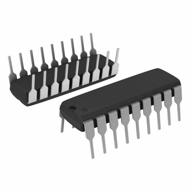


 工商网监
湘ICP备2023018690号
工商网监
湘ICP备2023018690号

