135 MHz Quad IF Receiver
AD6684
Data Sheet
FEATURES
4 integrated wideband digital downconverters (DDCs)
48-bit numerically controlled oscillator (NCO), up to
4 cascaded half-band filters
1.4 GHz analog input full power bandwidth
Amplitude detect bits for efficient automatic gain control
(AGC) implementation
Differential clock input
Integer clock divide by 1, 2, 4, or 8
On-chip temperature diode
Flexible JESD204B lane configurations
JESD204B (Subclass 1) coded serial digital outputs
Lane rates up to 15 Gbps
1.68 W total power at 500 MSPS
420 mW per analog-to-digital converter (ADC) channel
SFDR = 82 dBFS at 305 MHz (1.8 V p-p input range)
SNR = 66.8 dBFS at 305 MHz (1.8 V p-p input range)
Noise density = −151.5 dBFS/Hz (1.8 V p-p input range)
Analog input buffer
On-chip dithering to improve small signal linearity
Flexible differential input range
1.44 V p-p to 2.16 V p-p (1.80 V p-p nominal)
82 dB channel isolation/crosstalk
0.975 V, 1.8 V, and 2.5 V dc supply operation
Noise shaping requantizer (NSR) option for main receiver
Variable dynamic range (VDR) option for digital
predistortion (DPD)
APPLICATIONS
Communications
Diversity multiband, multimode digital receivers
3G/4G, W-CDMA, GSM, LTE, LTE-A
HFC digital reverse path receivers
Digital predistortion observation paths
General-purpose software radios
FUNCTIONAL BLOCK DIAGRAM
AVDD1 AVDD1_SR
(0.975V)
(0.975V)
VIN+A
BUFFER
ADC
CORE
VIN–A
AVDD2
(1.8V)
AVDD3
(2.5V)
DVDD
(0.975V)
DRVDD1
(0.975V)
FD_B
FAST
DETECT
DIGITAL DOWNCONVERTER
(×2)
ADC
CORE
VIN–B
NOISE SHAPED REQUANTIZER
(×2)
SIGNAL
MONITOR
BUFFER
VIN+B
SPIVDD
(1.8V)
SIGNAL PROCESSING
14
VCM_AB
FD_A
DRVDD2
(1.8V)
2
JESD204B
HIGH SPEED
SERIALIZER
Tx
OUTPUTS
SERDOUTAB0±
SERDOUTAB1±
VARIABLE DYNAMIC RANGE
(×2)
14
SIGNAL MONITOR
AND FAST DETECT
CLK–
SYSREF±
JESD204B
SUBCLASS 1
CONTROL
CLOCK
GENERATION
CLK+
SYNCINB±AB
SYNCINB±CD
÷2
÷4
÷8
VIN+C
ADC
CORE
VIN–C
VCM_CD
FD_C
SIGNAL PROCESSING
BUFFER
FAST
DETECT
14
DIGITAL DOWNCONVERTER
(×2)
SIGNAL
MONITOR
NOISE SHAPED REQUANTIZER
(×2)
JESD204B
HIGH SPEED
SERIALIZER
2
Tx
OUTPUTS
SERDOUTCD0±
SERDOUTCD1±
FD_D
VIN+D
BUFFER
ADC
CORE
VIN–D
14
VARIABLE DYNAMIC RANGE
(×2)
SPI CONTROL
AGND
DRGND
14994-001
PDWN/STBY
AD6684
SDIO SCLK CSB
Figure 1.
Rev. A
Document Feedback
Information furnished by Analog Devices is believed to be accurate and reliable. However, no
responsibility is assumed by Analog Devices for its use, nor for any infringements of patents or other
rights of third parties that may result from its use. Specifications subject to change without notice. No
license is granted by implication or otherwise under any patent or patent rights of Analog Devices.
Trademarks and registered trademarks are the property of their respective owners.
One Technology Way, P.O. Box 9106, Norwood, MA 02062-9106, U.S.A.
Tel: 781.329.4700
©2016-2020 Analog Devices, Inc. All rights reserved.
Technical Support
www.analog.com
�AD6684
Data Sheet
TABLE OF CONTENTS
Features .............................................................................................. 1
DDC Gain Stage ......................................................................... 44
Applications ....................................................................................... 1
DDC Complex to Real Conversion ......................................... 44
Functional Block Diagram .............................................................. 1
DDC Example Configurations ................................................. 45
Revision History ............................................................................... 3
Noise Shaping Requantizer (NSR) ............................................... 49
General Description ......................................................................... 4
Decimating Half-Band Filter .................................................... 49
Product Highlights ........................................................................... 4
NSR Overview ............................................................................ 50
Specifications..................................................................................... 5
Variable Dynamic Range (VDR) .................................................. 51
DC Specifications ......................................................................... 5
VDR Real Mode.......................................................................... 52
AC Specifications.......................................................................... 6
VDR Complex Mode ................................................................. 52
Digital Specifications ................................................................... 8
Digital Outputs ............................................................................... 54
Switching Specifications .............................................................. 9
Introduction to the JESD204B Interface ................................. 54
Timing Specifications .................................................................. 9
JESD204B Overview .................................................................. 54
Absolute Maximum Ratings .......................................................... 11
Functional Overview ................................................................. 56
Thermal Characteristics ............................................................ 11
JESD204B Link Establishment ................................................. 56
ESD Caution ................................................................................ 11
Physical Layer (Driver) Outputs .............................................. 57
Pin Configuration and Function Descriptions ........................... 12
JESD204B Tx Converter Mapping ........................................... 59
Typical Performance Characteristics ........................................... 14
Setting Up the AD6684 Digital Interface ................................ 60
Equivalent Circuits ......................................................................... 21
Latency ............................................................................................. 64
Theory of Operation ...................................................................... 23
End-To-End Total Latency ........................................................ 64
ADC Architecture ...................................................................... 23
Multichip Synchronization............................................................ 65
Analog Input Considerations.................................................... 23
SYSREF± Setup/Hold Window Monitor ................................. 67
Voltage Reference ....................................................................... 25
Test Modes ....................................................................................... 69
Clock Input Considerations ...................................................... 26
ADC Test Modes ........................................................................ 69
Temperature Diode .................................................................... 27
JESD204B Block Test Modes .................................................... 70
ADC Overrange and Fast Detect .................................................. 28
Serial Port Interface ........................................................................ 72
ADC Overrange .......................................................................... 28
Configuration Using the SPI ..................................................... 72
Fast Threshold Detection (FD_A, FD_B, FD_C and FD_D).... 28
Hardware Interface ..................................................................... 72
Signal Monitor ................................................................................ 29
SPI Accessible Features .............................................................. 72
SPORT Over JESD204B ............................................................. 29
Memory Map .................................................................................. 73
Digital Downconverter (DDC) ..................................................... 32
Reading the Memory Map Register Table............................... 73
DDC I/Q Input Selection .......................................................... 32
Memory Map .................................................................................. 74
DDC I/Q Output Selection ....................................................... 32
Memory Map Details ................................................................. 74
DDC General Description ........................................................ 32
Applications Information .............................................................. 98
Frequency Translation ................................................................... 38
Power Supply Recommendations............................................. 98
General Description ................................................................... 38
Exposed Pad Thermal Heat Slug Recommendations ............ 98
DDC NCO + Mixer Loss and SFDR ........................................ 39
AVDD1_SR (Pin 64) and AGND_SR (Pin 63 and Pin 67) ... 98
Numerically Controlled Oscillator........................................... 39
Outline Dimensions ....................................................................... 99
FIR Filters ........................................................................................ 41
Ordering Guide .......................................................................... 99
General Description ................................................................... 41
Half-Band Filters ........................................................................ 42
Rev. A | Page 2 of 99
�Data Sheet
AD6684
REVISION HISTORY
4/2020—Rev. 0 to Rev. A
Change to Unit Interval (UI) Parameter, Table 4 and Data Rate
per Channel (NRZ) Parameter, Table 4 .......................................... 9
Changes to De-Emphasis Section .................................................58
Added Table 33; Renumbered Sequentially and Figure 94;
Renumbered Sequentially ..............................................................58
Changes to Setting Up the AD6684 Digital Interface Section ..60
Changes to Example 1: ADC with DDC Option (Two ADCs
Plus Two DDCs in Each Pair) Section .........................................62
Changes to Figure 104 ....................................................................67
Changes to Reading the Memory Map Register Table Section .......73
Deleted Memory Map Summary Section and Table 45;
Renumbered Sequentially .............................................................. 74
Changes to Register 0x05B0 Row, Table 46 ................................. 94
Added Register 0x05C1 Rows, Table 46 ....................................... 95
Changes to Register 0x05C4 Row and Register 0x05C6 Row,
Table 46 ............................................................................................. 95
10/2016—Revision 0: Initial Version
Rev. A | Page 3 of 99
�AD6684
Data Sheet
GENERAL DESCRIPTION
The AD6684 is a 135 MHz bandwidth, quad intermediate
frequency (IF) receiver. It consists of four 14-bit, 500 MSPS
ADCs and various digital processing blocks consisting of four
wideband DDCs, an NSR, and VDR monitoring. The device has
an on-chip buffer and a sample-and-hold circuit designed for low
power, small size, and ease of use. This device is designed to
support communications applications. The analog full power
bandwidth of the device is 1.4 GHz.
The quad ADC cores feature a multistage, differential pipelined
architecture with integrated output error correction logic. Each
ADC features wide bandwidth inputs supporting a variety of
user-selectable input ranges. An integrated voltage reference
eases design considerations. The AD6684 is optimized for wide
input bandwidth, excellent linearity, and low power in a small
package.
The analog inputs and clock signal input are differential. Each
pair of ADC data outputs are internally connected to two DDCs
through a crossbar mux. Each DDC consists of up to five cascaded
signal processing stages: a 48-bit frequency translator, NCO, and
up to four half-band decimation filters.
Each ADC output is connected internally to an NSR block. The
integrated NSR circuitry allows improved SNR performance in
a smaller frequency band within the Nyquist bandwidth. The
device supports two different output modes selectable via the
serial port interface (SPI). With the NSR feature enabled, the
outputs of the ADCs are processed such that the AD6684
supports enhanced SNR performance within a limited portion
of the Nyquist bandwidth while maintaining a 9-bit output
resolution.
Each ADC output is also connected internally to a VDR block.
This optional mode allows full dynamic range for defined input
signals. Inputs that are within a defined mask (based on DPD
applications) are passed unaltered. Inputs that violate this
defined mask result in the reduction of the output resolution.
With VDR, the dynamic range of the observation receiver is
determined by a defined input frequency mask. For signals
falling within the mask, the outputs are presented at the
maximum resolution allowed. For signals exceeding defined
power levels within this frequency mask, the output resolution
is truncated. This mask is based on DPD applications and
supports tunable real IF sampling, and zero IF or complex IF
receive architectures.
Operation of the AD6684 in the DDC, NSR, and VDR modes is
selectable via SPI-programmable profiles (the default mode is
NSR at startup).
In addition to the DDC blocks, the AD6684 has several functions
that simplify the AGC function in the communications receiver.
The programmable threshold detector allows monitoring of the
incoming signal power using the fast detect output bits of the
ADC. If the input signal level exceeds the programmable threshold,
the fast detect indicator goes high. Because this threshold
indicator has low latency, the user can quickly turn down the
system gain to avoid an overrange condition at the ADC input.
Users can configure each pair of IF receiver outputs onto either
one or two lanes of Subclass 1 JESD204B-based high speed
serialized outputs, depending on the decimation ratio and the
acceptable lane rate of the receiving logic device. Multiple device
synchronization is supported through the SYSREF±,
SYNCINB±AB, and SYNCINB±CD input pins.
The AD6684 has flexible power-down options that allow
significant power savings when desired. All of these features can
be programmed using the 1.8 V capable, 3-wire SPI.
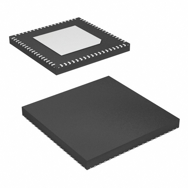
The AD6684 is available in a Pb-free, 72-lead LFCSP and is
specified over the −40°C to +105°C junction temperature range.
This product may be protected by one or more U.S. or international
patents
PRODUCT HIGHLIGHTS
1.
2.
3.
4.
5.
6.
7.
Rev. A | Page 4 of 99
Low power consumption per channel.
JESD204B lane rate support up to 15 Gbps.
Wide full power bandwidth supports IF sampling of signals
up to 1.4 GHz.
Buffered inputs ease filter design and implementation.
Four integrated wideband decimation filters and NCO
blocks supporting multiband receivers.
Programmable fast overrange detection.
On-chip temperature diode for system thermal management.
�Data Sheet
AD6684
SPECIFICATIONS
DC SPECIFICATIONS
AVDD1 = 0.975 V, AVDD1_SR = 0.975 V, AVDD2 = 1.8 V, AVDD3 = 2.5 V, DVDD = 0.975 V, DRVDD1 = 0.975 V, DRVDD2 = 1.8 V,
SPIVDD = 1.8 V, specified maximum sampling rate, clock divider = 4, 1.8 V p-p full-scale differential input, 0.5 V internal reference, AIN =
−1.0 dBFS, default SPI settings, unless otherwise noted. Minimum and maximum specifications are guaranteed for the full operating
TJ range of −40°C to +105°C. Typical specifications represent performance at TJ = 50°C (TA = 25°C).
Table 1.
Parameter
RESOLUTION
ACCURACY
No Missing Codes
Offset Error
Offset Matching
Gain Error
Gain Matching
Differential Nonlinearity (DNL)
Integral Nonlinearity (INL)
TEMPERATURE DRIFT
Offset Error
Gain Error
INTERNAL VOLTAGE REFERENCE
Voltage
INPUT REFERRED NOISE
ANALOG INPUTS
Differential Input Voltage Range (Programmable)
Common-Mode Voltage (VCM)
Differential Input Capacitance
Differential Input Resistance
Analog Input Full Power Bandwidth
POWER SUPPLY 1
AVDD1
AVDD1_SR
AVDD2
AVDD3
DVDD
DRVDD1
DRVDD2
SPIVDD
IAVDD1
IAVDD1_SR
IAVDD2
IAVDD3
IDVDD 2
IDRVDD1
IDRVDD2
ISPIVDD
POWER CONSUMPTION
Total Power Dissipation (Including Output Drivers)2
Power-Down Dissipation
Standby 3
Min
14
Typ
Max
Guaranteed
0
0
−5.0
+5.0
1.0
−0.7
−5.1
Power is measured at NSR, 28% bandwidth, L, M, and F = 222.
Default mode, no decimation enabled. For each link, L = 2, M = 2, and F = 2.
3
Standby mode is controlled by the SPI.
1
2
Rev. A | Page 5 of 99
±0.4
±1.0
+0.7
+5.1
Unit
Bits
% FSR
% FSR
% FSR
% FSR
LSB
LSB
8
214
ppm/°C
ppm/°C
0.5
2.6
V
LSB rms
1.44
1.80
1.34
1.75
200
1.4
2.16
V p-p
V
pF
Ω
GHz
0.95
0.95
1.71
2.44
0.95
0.95
1.71
1.71
0.975
0.975
1.8
2.5
0.975
0.975
1.8
1.8
319
21
438
87
145
162
23
1
1.00
1.00
1.89
2.56
1.00
1.00
1.89
1.89
482
53
473
103
198
207
29
1.6
V
V
V
V
V
V
V
V
mA
mA
mA
mA
mA
mA
mA
mA
1.68
325
1.20
1.94
W
mW
W
�AD6684
Data Sheet
AC SPECIFICATIONS
AVDD1 = 0.975 V, AVDD1_SR = 0.975 V, AVDD2 = 1.8 V, AVDD3 = 2.5 V, DVDD = 0.975 V, DRVDD1 = 0.975 V, DRVDD2 = 1.8 V,
SPIVDD = 1.8 V, specified maximum sampling rate, clock divider = 4, 1.8 V p-p full-scale differential input, 0.5 V internal reference, AIN =
−1.0 dBFS, default SPI settings, VDR mode (input mask not triggered), unless otherwise noted. Minimum and maximum specifications are
guaranteed for the full operating junction temperature (TJ) range of −40°C to +105°C. Typical specifications represent performance at TJ = 50°C
(TA = 25°C).
Table 2.
Parameter 1
ANALOG INPUT FULL SCALE
NOISE DENSITY 2
SIGNAL-TO-NOISE RATIO (SNR) 3
VDR Mode
fIN = 10 MHz
fIN = 155 MHz
fIN = 305 MHz
fIN = 450 MHz
fIN = 765 MHz
fIN = 985 MHz
21% Bandwidth (BW) Mode
(>105 MHz at 500 MSPS)
fIN = 10 MHz
fIN = 155 MHz
fIN = 305 MHz
fIN = 450 MHz
fIN = 765 MHz
fIN = 985 MHz
28% BW Mode (>135 MHz at
500 MSPS)
fIN = 10 MHz
fIN = 155 MHz
fIN = 305 MHz
fIN = 450 MHz
fIN = 765 MHz
fIN = 985 MHz
SIGNAL-TO-NOISE-AND-DISTORTION
RATIO (SINAD)3
fIN = 10 MHz
fIN = 155 MHz
fIN = 305 MHz
fIN = 450 MHz
fIN = 765 MHz
fIN = 985 MHz
EFFECTIVE NUMBER OF BITS (ENOB)3
fIN = 10 MHz
fIN = 155 MHz
fIN = 305 MHz
fIN = 450 MHz
fIN = 765 MHz
fIN = 985 MHz
Analog Input Full Scale =
1.44 V p-p
Min
Typ
Max
1.44
−149.7
65.4
65.3
65.2
65.0
64.8
64.5
Analog Input Full Scale =
1.80 V p-p
Min
Typ
Max
1.80
−151.5
Analog Input Full Scale =
2.16 V p-p
Min
Typ
Max
2.16
−153.0
Unit
V p-p
dBFS/Hz
67.1
67.0
66.8
66.6
66.5
66.0
68.4
68.3
68.0
67.8
67.5
66.9
dBFS
dBFS
dBFS
dBFS
dBFS
dBFS
72.1
71.8
71.9
71.6
71.0
70.6
73.8
73.5
73.5
73.2
72.7
72.1
75.1
74.8
74.7
74.4
73.7
73.0
dBFS
dBFS
dBFS
dBFS
dBFS
dBFS
69.6
69.1
69.1
69.4
68.5
68.5
71.3
70.8
70.7
71.0
70.2
70.0
72.6
72.1
71.9
72.2
71.2
70.9
dBFS
dBFS
dBFS
dBFS
dBFS
dBFS
67.0
66.8
66.6
66.4
66.1
65.5
68.2
67.9
67.6
67.3
66.9
66.2
dBFS
dBFS
dBFS
dBFS
dBFS
dBFS
10.8
10.8
10.7
10.7
10.6
10.6
11.0
10.9
10.9
10.8
10.8
10.7
Bits
Bits
Bits
Bits
Bits
Bits
65.3
65.2
65.1
65.0
64.7
64.2
10.5
10.5
10.5
10.5
10.4
10.3
64.8
64.5
10.4
Rev. A | Page 6 of 99
�Data Sheet
Parameter 1
SPURIOUS-FREE DYNAMIC RANGE
(SFDR)3
fIN = 10 MHz
fIN = 155 MHz
fIN = 305 MHz
fIN = 450 MHz
fIN = 765 MHz
fIN = 985 MHz
SPURIOUS-FREE DYNAMIC RANGE
(SFDR) AT −3 dBFS3
fIN = 10 MHz
fIN = 155 MHz
fIN = 305 MHz
fIN = 450 MHz
fIN = 765 MHz
fIN = 985 MHz
WORST HARMONIC, SECOND OR
THIRD3
fIN = 10 MHz
fIN = 155 MHz
fIN = 305 MHz
fIN = 450 MHz
fIN = 765 MHz
fIN = 985 MHz
WORST HARMONIC, SECOND OR
THIRD AT −3 dBFS3
fIN = 10 MHz
fIN = 155 MHz
fIN = 305 MHz
fIN = 450 MHz
fIN = 765 MHz
fIN = 985 MHz
WORST OTHER, EXCLUDING SECOND
OR THIRD HARMONIC3
fIN = 10 MHz
fIN = 155 MHz
fIN = 305 MHz
fIN = 450 MHz
fIN = 765 MHz
fIN = 985 MHz
TWO TONE INTERMODULATION
DISTORTION (IMD), AIN1 AND
AIN2 = −7 dBFS
fIN1 = 154 MHz, fIN2 = 157 MHz
fIN1 = 302 MHz, fIN2 = 305 MHz
CROSSTALK 4
FULL POWER BANDWIDTH 5
AD6684
Analog Input Full Scale =
1.44 V p-p
Min
Typ
Max
89
89
82
82
77
82
Analog Input Full Scale =
1.80 V p-p
Min
Typ
Max
Analog Input Full Scale =
2.16 V p-p
Min
Typ
Max
Unit
90
85
82
83
75
79
80
77
78
77
72
76
dBFS
dBFS
dBFS
dBFS
dBFS
dBFS
94
94
89
87
82
85
94
90
90
86
80
82
86
82
83
84
77
79
dBFS
dBFS
dBFS
dBFS
dBFS
dBFS
−89
−89
−82
−82
−77
−82
−90
−85
−82
−83
−75
−79
−80
−77
−78
−77
−72
−76
dBFS
dBFS
dBFS
dBFS
dBFS
dBFS
−94
−94
−89
−87
−82
−85
−94
−90
−90
−86
−80
−82
−86
−82
−83
−84
−77
−79
dBFS
dBFS
dBFS
dBFS
dBFS
dBFS
−96
−97
−97
−95
−92
−90
−98
−97
−98
−96
−91
−89
−99
−97
−97
−96
−88
−86
dBFS
dBFS
dBFS
dBFS
dBFS
dBFS
−93
−90
82
1.4
−90
−90
82
1.4
−84
−84
82
1.4
dBFS
dBFS
dB
GHz
75
−75
−86
See the AN-835 Application Note, Understanding High Speed ADC Testing and Evaluation, for definitions and for details on how these tests were completed.
Noise density is measured with no analog input signal.
See Table 9 for recommended settings for full-scale voltage and buffer current setting.
4
Crosstalk is measured at 155 MHz with a −1.0 dBFS analog input on one channel and no input on the adjacent channel.
5
Measured with circuit shown in Figure 58.
1
2
3
Rev. A | Page 7 of 99
�AD6684
Data Sheet
DIGITAL SPECIFICATIONS
AVDD1 = 0.975 V, AVDD1_SR = 0.975 V, AVDD2 = 1.8 V, AVDD3 = 2.5 V, DVDD = 0.975 V, DRVDD1 = 0.975 V, DRVDD2 = 1.8 V,
SPIVDD = 1.8 V, specified maximum sampling rate, clock divider = 4, 1.8 V p-p full-scale differential input, 0.5 V internal reference, AIN =
−1.0 dBFS, default SPI settings, unless otherwise noted. Minimum and maximum specifications are guaranteed for the full operating junction
temperature (TJ) range of −40°C to +105°C. Typical specifications represent performance at TJ = 50°C (TA = 25°C).
Table 3.
Parameter
CLOCK INPUTS (CLK+, CLK−)
Logic Compliance
Differential Input Voltage
Input Common-Mode Voltage
Input Resistance (Differential)
Input Capacitance
SYSREF INPUTS (SYSREF+, SYSREF−) 1
Logic Compliance
Differential Input Voltage
Input Common-Mode Voltage
Input Resistance (Differential)
Input Capacitance (Single-Ended per Pin)
LOGIC INPUTS (PDWN/STBY)
Logic Compliance
Logic 1 Voltage
Logic 0 Voltage
Input Resistance
LOGIC INPUTS (SDIO, SCLK, CSB)
Logic Compliance
Logic 1 Voltage
Logic 0 Voltage
Input Resistance
LOGIC OUTPUT (SDIO)
Logic Compliance
Logic 1 Voltage (IOH = 800 µA)
Logic 0 Voltage (IOL = 50 µA)
SYNCIN INPUT (SYNCINB+AB, SYNCINB−AB, SYNCINB+CD, SYNCINB−CD)
Logic Compliance
Differential Input Voltage
Input Common-Mode Voltage
Input Resistance (Differential)
Input Capacitance (Single-Ended per Pin)
LOGIC OUTPUTS (FD_A, FD_B)
Logic Compliance
Logic 1 Voltage
Logic 0 Voltage
Input Resistance
DIGITAL OUTPUTS (SERDOUTx±, x = AB0, AB1, CD0, and CD1)
Logic Compliance
Differential Output Voltage
Short-Circuit Current (ID SHORT)
Differential Termination Impedance
1
Min
Typ
400
400
0.6
18
Max
Unit
LVDS/LVPECL
800
1600
0.69
32
0.9
mV p-p
V
kΩ
pF
LVDS/LVPECL
800
1800
0.69
2.2
22
0.7
mV p-p
V
kΩ
pF
CMOS
0.65 × SPIVDD
0
0.35 × SPIVDD
V
V
MΩ
0.35 × SPIVDD
V
V
kΩ
10
CMOS
0.65 × SPIVDD
0
56
CMOS
SPIVDD − 0.45 V
0
400
0.6
18
0.45
LVDS/LVPECL/CMOS
800
1800
0.69
2.2
22
0.7
V
V
mV p-p
V
kΩ
pF
CMOS
0.8 × SPIVDD
0
DC-coupled input only.
Rev. A | Page 8 of 99
56
V
V
kΩ
CML
455.8
15
100
mV p-p
mA
Ω
0.5
�Data Sheet
AD6684
SWITCHING SPECIFICATIONS
AVDD1 = 0.975 V, AVDD1_SR = 0.975 V, AVDD2 = 1.8 V, AVDD3 = 2.5 V, DVDD = 0.975 V, DRVDD1 = 0.975 V, DRVDD2 = 1.8 V,
SPIVDD = 1.8 V, specified maximum sampling rate, clock divider = 4, 1.8 V p-p full-scale differential input, 0.5 V internal reference, AIN =
−1.0 dBFS, default SPI settings, unless otherwise noted. Minimum and maximum specifications are guaranteed for the full operating junction
temperature (TJ) range of −40°C to +105°C. Typical specifications represent performance at TJ = 50°C (TA = 25°C).
Table 4.
Parameter
CLOCK
Clock Rate at CLK+/CLK− Pins
Maximum Sample Rate 1
Minimum Sample Rate 2
Clock Pulse Width High
Clock Pulse Width Low
OUTPUT PARAMETERS
Unit Interval (UI) 3
Rise Time (tR) (20% to 80% into 100 Ω Load)
Fall Time (tF) (20% to 80% into 100 Ω Load)
Phase-Locked Loop (PLL) Lock Time
Data Rate per Channel (NRZ) 4
LATENCY 5
Pipeline Latency
Fast Detect Latency
APERTURE
Aperture Delay (tA)
Aperture Uncertainty (Jitter, tj)
Out-of-Range Recovery Time
Min
Typ
0.3
500
240
125
125
66.67
1.6875
100
31.25
31.37
5
10
Max
Unit
2.4
GHz
MSPS
MSPS
ps
ps
15
ps
ps
ps
ms
Gbps
30
Sample clock cycles
Sample clock cycles
54
160
44
1
ps
fs rms
Sample clock cycles
The maximum sample rate is the clock rate after the divider.
The minimum sample rate operates at 240 MSPS with L = 2 or L = 1. Refer to SPI Register 0x011A to reduce the threshold of the clock detect circuit.
3
Baud rate = 1/UI. A subset of this range can be supported.
4
Default L = 2. This number can be changed based on the sample rate and decimation ratio.
5
No DDCs used. L = 2, M = 2, F = 2 for each link.
1
2
TIMING SPECIFICATIONS
Table 5.
Parameter
CLK+ to SYSREF+ TIMING REQUIREMENTS
tSU_SR
tH_SR
SPI TIMING REQUIREMENTS
tDS
tDH
tCLK
tS
tH
tHIGH
tLOW
tACCESS
tDIS_SDIO
Test Conditions/Comments
See Figure 3
Device clock to SYSREF+ setup time
Device clock to SYSREF+ hold time
See Figure 4
Setup time between the data and the rising edge of SCLK
Hold time between the data and the rising edge of SCLK
Period of the SCLK
Setup time between CSB and SCLK
Hold time between CSB and SCLK
Minimum period that SCLK must be in a logic high state
Minimum period that SCLK must be in a logic low state
Maximum time delay between falling edge of SCLK and output
data valid for a read operation
Time required for the SDIO pin to switch from an output to an
input relative to the CSB rising edge (not shown in Figure 4)
Rev. A | Page 9 of 99
Min
Typ
Max
−44.8
64.4
ps
ps
6
ns
ns
ns
ns
ns
ns
ns
ns
4
2
40
2
2
10
10
10
Unit
10
ns
�AD6684
Data Sheet
Timing Diagrams
APERTURE
DELAY
SAMPLE N
N – 53
N+1
N – 54
N – 52
N – 51
N–1
N – 50
14994-002
ANALOG
INPUT
SIGNAL
CLK–
CLK+
Figure 2. Data Output Timing (NSR Mode, 21%, L, M, F = 222)
CLK–
CLK+
tSU_SR
tH_SR
14994-003
SYSREF–
SYSREF+
Figure 3. SYSREF± Setup and Hold Timing
tHIGH
tDS
tS
tCLK
tDH
tACCESS
tH
tLOW
CSB
SDIO DON’T CARE
DON’T CARE
R/W
A14
A13
A12
A11
A10
A9
A8
A7
D7
Figure 4. Serial Port Interface Timing Diagram
Rev. A | Page 10 of 99
D6
D3
D2
D1
D0
DON’T CARE
14994-004
SCLK DON’T CARE
�Data Sheet
AD6684
ABSOLUTE MAXIMUM RATINGS
THERMAL CHARACTERISTICS
Table 6.
Parameter
Electrical
AVDD1 to AGND
AVDD1_SR to AGND
AVDD2 to AGND
AVDD3 to AGND
DVDD to DGND
DRVDD1 to DRGND
DRVDD2 to DRGND
SPIVDD to AGND
VIN±x to AGND
CLK± to AGND
SCLK, SDIO, CSB to DGND
PDWN/STBY to DGND
SYSREF± to AGND_SR
SYNCIN±AB/SYNCIN±CD to DRGND
Environmental
Operating Junction Temperature
Range
Maximum Junction Temperature
Storage Temperature Range
(Ambient)
Rating
1.05 V
1.05 V
2.00 V
2.70 V
1.05 V
1.05 V
2.00 V
2.00 V
−0.3 V to AVDD3 + 0.3 V
−0.3 V to AVDD1 + 0.3 V
−0.3 V to SPIVDD + 0.3 V
−0.3 V to SPIVDD + 0.3 V
0 V to 2.5 V
0 V to 2.5 V
Thermal performance is directly linked to printed circuit board
(PCB) design and operating environment. Careful attention to
PCB thermal design is required.
Table 7. Thermal Resistance
PCB Type
JEDEC
2s2p Board
10-Layer Board
Airflow Velocity
(m/sec)
0.0
1.0
2.5
0.0
θJA
21.58
17.94 1, 2
16.58 1, 2
1, 2
9.74
θJCB
1.951, 3
N/A4
N/A4
1.00
Per JEDEC 51-7, plus JEDEC 51-5 2s2p test board.
Per JEDEC JESD51-2 (still air) or JEDEC JESD51-6 (moving air).
3
Per MIL-STD 883, Method 1012.1.
4
N/A means not applicable.
1
2
ESD CAUTION
−40°C to +105°C
125°C
−65°C to +150°C
Stresses at or above those listed under Absolute Maximum
Ratings may cause permanent damage to the product. This is a
stress rating only; functional operation of the product at these
or any other conditions above those indicated in the operational
section of this specification is not implied. Operation beyond the
maximum operating conditions for extended periods may affect
product reliability.
Rev. A | Page 11 of 99
Unit
°C/W
°C/W
°C/W
°C/W
�AD6684
Data Sheet
72
71
70
69
68
67
66
65
64
63
62
61
60
59
58
57
56
55
AVDD2
AVDD1
AVDD1
AVDD1
AVDD1
AGND_SR
SYSREF–
SYSREF+
AVDD1_SR
AGND_SR
AVDD1
CLK–
CLK+
AVDD1
AVDD1
AVDD1
AVDD1
AVDD2
PIN CONFIGURATION AND FUNCTION DESCRIPTIONS
1
2
3
4
5
6
7
8
9
10
11
12
13
14
15
16
17
18
54
53
52
51
50
49
48
47
46
45
44
43
42
41
40
39
38
37
AD6684
TOP VIEW
(Not to Scale)
AVDD3
VIN–C
VIN+C
AVDD2
AVDD2
AVDD3
VIN+D
VIN–D
AVDD2
AVDD1
AVDD1
VCM_CD/VREF
DVDD
DGND
SPIVDD
CSB
SCLK
SDIO
NOTES
1. EXPOSED PAD. ANALOG GROUND. THE EXPOSED THERMAL PAD ON THE BOTTOM OF THE PACKAGE
PROVIDES THE GROUND REFERENCE FOR AVDDx, SPIVDD, DVDD, DRVDD1, AND DRVDD2.
THIS EXPOSED PAD MUST BE CONNECTED TO GROUND FOR PROPER OPERATION.
14994-005
SYNCINB–AB
SYNCINB+AB
DRGND
DRVDD1
SERDOUTAB0–
SERDOUTAB0+
SERDOUTAB1–
SERDOUTAB1+
SERDOUTCD1+
SERDOUTCD1–
SERDOUTCD0+
SERDOUTCD0–
DRVDD1
DRGND
SYNCINB+CD
SYNCINB–CD
FD_D
FD_C
19
20
21
22
23
24
25
26
27
28
29
30
31
32
33
34
35
36
AVDD3
VIN–A
VIN+A
AVDD2
AVDD2
AVDD3
VIN+B
VIN–B
AVDD2
AVDD1
AVDD1
VCM_AB
DVDD
DGND
DRVDD2
PDWN/STBY
FD_A
FD_B
Figure 5. Pin Configuration (Top View)
Table 8. Pin Function Descriptions
Pin No.
0
Mnemonic
AGND/EPAD
Type
Ground
1, 6, 49, 54
2, 3
4, 5, 9, 46, 50, 51, 55, 72
7, 8
10, 11, 44, 45, 56, 57, 58, 59,
62, 68, 69, 70, 71
12
AVDD3
VIN−A, VIN+A
AVDD2
VIN+B, VIN−B
AVDD1
Supply
Input
Supply
Input
Supply
VCM_AB
Output
13, 42
14, 41
15
16
DVDD
DGND
DRVDD2
PDWN/STBY
Supply
Ground
Supply
Input
17, 18, 36, 35
FD_A, FD_B, FD_C, FD_D
Output
19
SYNCINB−AB
Input
20
SYNCINB+AB
Input
21, 32
22, 31
DRGND
DRVDD1
Ground
Supply
Description
Exposed Pad. Analog Ground. The exposed thermal pad on
the bottom of the package provides the ground reference for
AVDDx, SPIVDD, DVDD, DRVDD1, and DRVDD2. This exposed
pad must be connected to ground for proper operation.
Analog Power Supply (2.5 V Nominal).
ADC A Analog Input Complement/True.
Analog Power Supply (1.8 V Nominal).
ADC B Analog Input True/Complement.
Analog Power Supply (0.975 V Nominal).
Common-Mode Level Bias Output for Analog Input Channel A
and Channel B
Digital Power Supply (0.975 V Nominal).
Ground Reference for DVDD and SPIVDD.
Digital Power Supply for JESD204B PLL (1.8 V Nominal).
Power-Down Input (Active High). The operation of this pin
depends on the SPI mode and can be configured as powerdown or standby. Requires external 10 kΩ pull-down resistor.
Fast Detect Outputs for Channel A, Channel B, Channel C, and
Channel D.
Active Low JESD204B LVDS Sync Input Complement for
Channel A and Channel B.
Active Low JESD204B LVDS/CMOS Sync Input True for Channel A
and Channel B.
Ground Reference for DRVDD1 and DRVDD2.
Digital Power Supply for SERDOUT Pins (0.975 V Nominal).
Rev. A | Page 12 of 99
�Data Sheet
Pin No.
23, 24
AD6684
Type
Output
33
Mnemonic
SERDOUTAB0−,
SERDOUTAB0+
SERDOUTAB1−,
SERDOUTAB1+
SERDOUTCD1+,
SERDOUTCD1−
SERDOUTCD0+,
SERDOUTCD0−
SYNCINB+CD
34
SYNCINB−CD
Input
37
38
39
40
43
SDIO
SCLK
CSB
SPIVDD
VCM_CD/VREF
Input/output
Input
Input
Supply
Output/input
47, 48
52, 53
60, 61
63, 67
64
65, 66
VIN−D, VIN+D
VIN+C, VIN−C
CLK+, CLK−
AGND_SR
AVDD1_SR
SYSREF+, SYSREF−
Input
Input
Input
Ground
Supply
Input
25, 26
27, 28
29, 30
Output
Output
Output
Input
Description
Lane 0 Output Data Complement/True for Channel A and
Channel B.
Lane 1 Output Data Complement/True for Channel A and
Channel B.
Lane 1 Output Data True/Complement for Channel C and
Channel D.
Lane 0 Output Data True/Complement for Channel C and
Channel D.
Active Low JESD204B LVDS/CMOS Sync Input True for Channel C
and Channel D.
Active Low JESD204B LVDS Sync Input Complement for
Channel C and Channel D.
SPI Serial Data Input/Output.
SPI Serial Clock.
SPI Chip Select (Active Low).
Digital Power Supply for SPI (1.8 V Nominal).
Common-Mode Level Bias Output for Analog Input Channel C
and Channel D/0.5 V Reference Voltage Input. This pin is
configurable through the SPI as an output or an input. Use
this pin as the common-mode level bias output if using the
internal reference. This pin requires a 0.5 V reference voltage
input if using an external voltage reference source.
ADC D Analog Input Complement/True.
ADC C Analog Input True/Complement.
Clock Input True/Complement.
Ground Reference for SYSREF±.
Analog Power Supply for SYSREF± (0.975 V Nominal).
Active Low JESD204B LVDS System Reference (SYSREF) Input
True/Complement. DC-coupled input only.
Rev. A | Page 13 of 99
�AD6684
Data Sheet
TYPICAL PERFORMANCE CHARACTERISTICS
AVDD1 = 0.975 V, AVDD1_SR = 0.975 V, AVDD2 = 1.8 V, AVDD3 = 2.5 V, DVDD = 0.975 V, DRVDD1 = 0.975 V, DRVDD2 = 1.8 V,
SPIVDD = 1.8 V, specified maximum sampling rate, clock divider = 4, 1.5 V p-p full-scale differential input, AIN = −1.0 dBFS, default SPI
settings, VDR mode (input mask not triggered), unless otherwise noted. Minimum and maximum specifications are guaranteed for the full
operating junction temperature (TJ) range of −40°C to +105°C. Typical specifications represent performance at TJ = 50°C (TA = 25°C).
–20
AMPLITUDE (dBFS)
–40
–60
–80
–40
–60
–80
–100
–100
–120
–120
50
100
150
200
250
FREQUENCY (MHz)
–140
14994-100
–140
0
AIN = –1dBFS
SNR = 66.8dB
SFDR = 82dBFS
ENOB = 10.7 BITS
0
100
150
AIN = –1dBFS
SNR = 67.0dB
SFDR = 85dBFS
ENOB = 10.8 BITS
–20
AMPLITUDE (dBFS)
–60
–80
–40
–60
–80
–100
–100
–120
–120
100
150
200
FREQUENCY (MHz)
250
–140
14994-101
–140
50
AIN = –1dBFS
SNR = 66.6dB
SFDR = 83dBFS
ENOB = 10.7 BITS
–20
–40
0
250
Figure 8. Single-Tone FFT with fIN = 305 MHz
0
0
200
FREQUENCY (MHz)
Figure 6. Single-Tone FFT with fIN = 10.3 MHz
AMPLITUDE (dBFS)
50
14994-102
–20
AMPLITUDE (dBFS)
0
AIN = –1dBFS
SNR = 67.10dB
SFDR = 90dBFS
ENOB = 10.8 BITS
0
50
100
150
200
FREQUENCY (MHz)
Figure 9. Single-Tone FFT with fIN = 453 MHz
Figure 7. Single-Tone FFT with fIN = 155 MHz
Rev. A | Page 14 of 99
250
14994-103
0
�Data Sheet
95
0
AIN = –1dBFS
SNR = 66.5dB
SFDR = 75dBFS
ENOB = 10.6 BITS
–20
90
–40
85
SNR/SFDR (dBFS)
–100
70
–120
65
565
ANALOG INPUT FREQUENCY (MHz)
Figure 10. Single-Tone FFT with fIN = 765 MHz
0
67.5
67.4
67.3
67.2
67.1
–40
67.0
–60
SNR (dBFS)
AMPLITUDE (dBFS)
Figure 13. SNR/SFDR vs. Analog Input Frequency (fIN)
AIN = –1dBFS
SNR = 66.0dB
SFDR = 79dBFS
ENOB = 10.6 BITS
–20
14994-107
465
365
265
245
225
60
205
FREQUENCY (MHz)
SNRFS, –40°C
SNRFS, +50°C
SNRFS, +105°C
185
250
200
165
150
145
100
125
50
85
0
14994-104
–140
SFDR (dBFS), –40°C
SFDR (dBFS), +50°C
SFDR (dBFS), +105°C
75
105
–80
80
65
–60
10
AMPLITUDE (dBFS)
AD6684
–80
66.9
66.8
66.7
66.6
66.5
–100
66.4
66.3
–120
66.2
66.1
465
ANALOG INPUT FREQUENCY (MHz)
14994-108
365
265
245
225
205
185
165
66.0
145
FREQUENCY (MHz)
125
250
200
105
150
85
100
65
50
10
0
14994-105
–140
Figure 14. SNR vs. Analog Input Frequency (fIN), First and Second Nyquist
Zones; AIN at −3 dBFS
Figure 11. Single-Tone FFT with fIN = 985 MHz
94
90
93
92
85
SFDR
91
SFDR (dBFS)
89
75
70
88
87
86
85
84
SNR
83
65
82
81
Figure 12. SNR/SFDR vs. Sample Rate (fS), fIN = 155 MHz
465
365
14994-109
ANALOG INPUT FREQUENCY (MHz)
265
245
225
205
185
165
145
125
105
85
10
650
14994-106
625
600
575
525
550
500
475
450
425
400
375
325
350
300
275
250
225
200
SAMPLE RATE (MHz)
65
80
60
175
SNR/SFDR (dBFS)
90
80
Figure 15. SFDR vs. Analog Input Frequency (fIN), First and Second Nyquist
Zones; AIN at −3 dBFS
Rev. A | Page 15 of 99
�AD6684
Data Sheet
0
67.5
AIN1 AND AIN2 = –7dBFS
SFDR = 85.9dBFS
–20
AMPLITUDE (dBFS)
–40
SNR (dBFS)
67.0
66.5
–60
–80
–100
–120
–140
795
14994-110
765
735
705
675
645
615
585
555
525
495
465
ANALOG INPUT FREQUENCY (MHz)
0
50
100
150
14994-113
–160
66.0
250
200
FREQUENCY (MHz)
Figure 16. SNR vs. Analog Input Frequency (fIN), Third Nyquist Zone
AIN at −3 dBFS
Figure 19. Two Tone FFT; fIN1 = 303.5 MHz, fIN2 = 306.5 MHz
94
0
93
92
–20
SFDR/IMD3 (dBc AND dBFS)
91
90
SFDR (dBFS)
89
88
87
86
85
84
83
82
SFDR (dBc)
–40
IMD3 (dBc)
–60
–80
SFDR (dBFS)
–100
–120
IMD3 (dBFS)
ANALOG INPUT AMPLITUDE (dBFS)
Figure 17. SFDR vs. Analog Input Frequency (fIN), Third Nyquist Zone; AIN
at −3 dBFS
Figure 20. Two Tone SFDR/IMD3 vs. Analog Input Amplitude (AIN) with
fIN1 = 303.5 MHz and fIN2 = 306.5 MHz
0
AIN1 AND AIN2 = –7dBFS
SFDR = 86.4dBFS
–20
SNR/SFDR (dB)
–60
–80
–100
–120
–140
0
50
100
150
200
FREQUENCY (MHz)
250
14994-112
AMPLITUDE (dBFS)
–40
–160
0
120
110
100
90
80
70
60
50
40
30
20
10
0
–10
–20
–30
–40
–100
SFDR (dBFS)
SNRFS
SFDR (dBc)
SNR
–90
–80 –70 –60 –50 –40 –30 –20
ANALOG INPUT FREQUENCY (MHz)
–10
0
Figure 21. SNR/SFDR vs. Analog Input Frequency, fIN = 155 MHz
Figure 18. Two Tone FFT; fIN1 = 153.5 MHz, fIN2 = 156.5 MHz
Rev. A | Page 16 of 99
14994-115
735
ANALOG INPUT FREQUENCY (MHz)
–140
–90 –84 –78 –72 –66 –60 –54 –48 –42 –36 –30 –24 –18 –12
14994-111
705
675
645
615
585
555
525
495
465
80
14994-114
81
�Data Sheet
1.0
SFDR (dBFS)
0.8
0.6
SNRFS
0.4
0.2
DNL (LSB)
SFDR (dBc)
SNR
0
–0.2
–0.4
–0.6
16384
14994-119
15360
14336
13312
12288
11264
9216
10240
8192
7168
6144
5120
–1.0
4096
0
3072
–10
2048
–80 –70 –60 –50 –40 –30 –20
ANALOG INPUT FREQUENCY (MHz)
0
–90
1024
–0.8
14994-116
SNR/SFDR (dB)
120
110
100
90
80
70
60
50
40
30
20
10
0
–10
–20
–30
–40
–100
AD6684
OUTPUT CODE
Figure 22. SNR/SFDR vs. Analog Input Frequency, fIN = 305 MHz
Figure 25. DNL, fIN = 10.3 MHz
90
6000
5000
80
4000
NUMBER OF HITS
85
SNR
2000
129
JUNCTION TEMPERATURE (°C)
14994-117
122
111
91
71
–10
51
0
31
60
11
1000
–31
65
CODE
Figure 23. SNR/SFDR vs. Junction Temperature, fIN = 155 MHz
Figure 26. Input-Referred Noise Histogram
2.1
2.0
1.5
POWER DISSIPATION (W)
2.0
0.5
0
–0.5
–1.0
1.9
1.8
1.7
1.6
Figure 24. INL, fIN = 10.3 MHz
16384
15360
14336
13312
–38
–21
8
20
43
49
59
TEMPERATURE (°C)
14994-118
OUTPUT CODE
12288
11264
10240
9216
8192
7168
6144
5120
4096
3072
2048
1.5
0
–2.0
81
100
115
14994-121
–1.5
1024
INL (LSB)
1.0
Figure 27. NSR Mode Power Dissipation vs. Junction Temperature
Rev. A | Page 17 of 99
14994-120
70
3000
N – 10
N–9
N–8
N–7
N–6
N–5
N–4
N–3
N–2
N–1
0
N+1
N+2
N+3
N+4
N+5
N+6
N+7
N+8
N+9
N + 10
75
–54
SNR/SFRDR (dBFS)
SFDR
�Data Sheet
1.85
0
1.80
–20
1.75
1.70
NSR
1.65
1.60
1.55
–60
–80
–100
–120
1.50
250
300
350
500
400
450
SAMPLE RATE (MSPS)
550
600
650
–1.25
8.75
0
18.75
28.75
AIN = –1dBFS
SNRFS = 74.50dB
SFDR = 100.68dBFS
–20
–40
–60
–80
–100
–60
–80
–100
–120
–120
–140
–140
–75
–25
25
FREQUENCY (MHz)
75
125
–160
–15.625
14994-123
–160
–125
Figure 29. DDC Mode (4 DDCs, DCM2, L, M, and F = 244) with fIN = 305 MHz
–10.625
4.375
9.375
14.375
Figure 32. DDC Mode (4 DDCs, Decimate by 16, L, M, and F = 148) with
fIN = 305 MHz
AIN = –1dBFS
SNRFS = 71.80dB
SFDR = 98.27dBFS
–20
–0.625
FREQUENCY (MHz)
0
0
–5.625
14994-126
AMPLITUDE (dBFS)
–40
AIN = –1dBFS
SNRFS = 74.50dB
SFDR = 100.68dBFS
–20
–40
AMPLITUDE (dBFS)
–40
–60
–80
–100
–60
–80
–100
–120
–120
–140
–140
–160
57.5
62.5
5
14994-124
FREQUENCY (MHz)
37.5
17.5
0
–22.5
–42.5
–62.5
–160
Figure 30. DDC Mode (4 DDCs, Decimate by 4, L, M, and F = 148) with
fIN = 305 MHz
25
45
65
85
FREQUENCY (MHz)
105
125
14994-127
AMPLITUDE (dBFS)
–11.25
FREQUENCY (MHz)
AIN = –1dBFS
SNRFS = 65.94dB
SFDR = 89.01dBFS
–20
–21.25
Figure 31. DDC Mode (4 DDCs, Decimate by 8, L, M, and F = 148) with
fIN = 305 MHz
Figure 28. Power Dissipation vs. Sample Rate (fS)
0
–160
–31.25
14994-122
1.40
14994-125
–140
1.45
AMPLITUDE (dBFS)
AIN = –1dBFS
SNRFS = 71.80dB
SFDR = 98.27dBFS
–40
AMPLITUDE (dBFS)
POWER DISSIPATION (W)
AD6684
Figure 33. NSR Mode (Decimate by 2, L, M, and F = 124) with fIN = 305 MHz
Rev. A | Page 18 of 99
�Data Sheet
AD6684
Figure 37. SFDR vs. Analog Input Frequency with Different Buffer Current
Settings (Third Nyquist Zone)
67.0
66.9
66.8
66.7
66.6
SFDR (dBFS)
66.4
66.3
66.2
66.1
66.0
65.9
65.8
65.7
65.6
DIFFERENTIAL VOLTAGE (V)
ANALOG INPUT FREQUENCY (MHz)
Figure 35. SNR vs. Clock Amplitude (Differential Voltage), fIN = 155.3 MHz
Figure 38. SFDR vs. Analog Input Frequency with Different Buffer Current
Settings (Fourth Nyquist Zone)
69
= 160µA
= 200µA
= 240µA
= 280µA
INPUT FULL SCALE = 2.16V
68
SNR (dBFS)
BUFFER CURRENT
BUFFER CURRENT
BUFFER CURRENT
BUFFER CURRENT
67
66
INPUT FULL SCALE = 1.44V
65
465
365
14994-133
ANALOG INPUT FREQUENCY (MHz)
Figure 36. SFDR vs. Analog Input Frequency with Different Buffer Current
Settings (First and Second Nyquist Zones)
265
245
225
205
185
165
145
125
105
85
10
465
365
14994-130
ANALOG INPUT FREQUENCY (MHz)
265
245
225
205
185
165
145
125
105
85
65
64
10
SFDR (dBFS)
= 320µA
= 360µA
= 400µA
= 440µA
730
760
790
820
850
880
910
940
970
1030
1060
1090
1120
1150
1180
1210
1240
1270
1300
1330
1360
1390
1420
1450
1480
1510
1540
1570
1600
1630
1660
1690
1720
1750
1780
1810
14994-129
0.118
0.132
0.148
0.166
0.185
0.207
0.234
0.262
0.293
0.328
0.370
0.416
0.468
0.526
0.587
0.693
0.778
0.873
0.979
1.091
1.209
1.322
1.482
1.653
1.833
65.5
BUFFER CURRENT
BUFFER CURRENT
BUFFER CURRENT
BUFFER CURRENT
65
SNR (dBFS)
66.5
–80
–78
–76
–74
–72
–70
–68
–66
–64
–62
–60
–58
–56
–54
–52
–50
–48
–46
–44
–42
–40
14994-132
Figure 34. NSR Mode (LMF = 222) with fIN = 305 MHz
–95
–94
–93
–92
–91
–90
–89
–88
–87
–86
–85
–84
–83
–82
–81
–80
–79
–78
–77
–76
–75
735
ANALOG INPUT FREQUENCY (MHz)
14994-131
465
250
FREQUENCY (MHz)
14994-128
225
200
175
150
125
100
75
50
25
0
–140
705
–120
= 200µA
= 240µA
= 280µA
= 320µA
675
–100
BUFFER CURRENT
BUFFER CURRENT
BUFFER CURRENT
BUFFER CURRENT
645
–80
615
–60
585
SFDR (dBFS)
AMPLITUDE (dBFS)
–40
555
–20
–85
–84
–83
–82
–81
–80
–79
–78
–77
–76
–75
–74
–73
–72
–71
–70
–69
–68
–67
–66
–65
525
AIN = –1dBFS
SNRFS = 70.7dB
SFDR = 82dBFS
495
0
Figure 39. SNR vs. Analog Input Frequency with Different Analog Input
Full Scales (First and Second Nyquist Zones)
Rev. A | Page 19 of 99
�Data Sheet
565
14994-136
465
365
265
245
225
205
185
165
145
795
14994-137
765
735
705
675
645
ANALOG INPUT FREQUENCY (MHz)
Figure 43. SFDR vs. Analog Input Frequency with Different Analog Input
Full Scales (Third Nyquist Zone)
–81
INPUT FULL SCALE = 1.44V
–79
–77
–75
–73
SFDR (dBFS)
–71
–69
INPUT FULL SCALE = 2.16V
–67
–65
–63
–61
–59
1780
1720
1660
14994-138
ANALOG INPUT FREQUENCY (MHz)
1600
1540
1480
1420
1360
1300
1240
1180
1120
970
1060
–55
910
–57
850
Figure 41. SNR vs. Analog Input Frequency with Different Analog Input
Full Scales (Fourth Nyquist Zone)
615
465
14994-135
730
760
790
820
850
880
910
940
970
1000
1030
1060
1090
1120
1150
1180
1210
1240
1270
1300
1330
1360
1390
1420
1450
1480
1510
1540
1570
1600
1630
1660
1690
1720
1750
1780
1810
62
585
63
INPUT FULL SCALE = 2.16V
555
64
INPUT FULL SCALE = 1.44V
525
SFDR (dBFS)
SNR (dBFS)
66
–90
–89
–88
–87
–86
–85
–84
–83
–82
–81
–80
–79
–78
–77
–76
–75
–74
–73
–72
–71
–70
495
INPUT FULL SCALE = 2.16V
INPUT FULL SCALE = 1.44V
125
Figure 42. SFDR vs. Analog Input Frequency with Different Analog Input
Full Scales (First and Second Nyquist Zones)
68
ANALOG INPUT FREQUENCY (MHz)
85
ANALOG INPUT FREQUENCY (MHz)
790
Figure 40. SNR vs. Analog Input Frequency with Different Analog Input
Full Scales (Third Nyquist Zone)
65
105
10
735.3
ANALOG INPUT FREQUENCY (MHz)
67
INPUT FULL SCALE = 2.16V
14994-134
705.3
675.3
645.3
615.3
585.3
555.3
525.3
495.3
INPUT FULL SCALE = 1.44V
INPUT FULL SCALE = 1.44V
65
SFDR (dBFS)
INPUT FULL SCALE = 2.16V
–90
–89
–88
–87
–86
–85
–84
–83
–82
–81
–80
–79
–78
–77
–76
–75
–74
–73
–72
–71
–70
730
69.0
68.8
68.6
68.4
68.2
68.0
67.8
67.6
67.4
67.2
67.0
66.8
66.6
66.4
66.2
66.0
65.8
65.6
65.4
65.2
65.0
64.8
64.6
64.4
64.2
64.0
465.3
SNR (dBFS)
AD6684
Figure 44. SFDR vs. Analog Input Frequency with Different Analog Input
Full Scales (Fourth Nyquist Zone)
Rev. A | Page 20 of 99
�Data Sheet
AD6684
EQUIVALENT CIRCUITS
AVDD3
AVDD3
VIN+x
3.5pF
AVDD3
100Ω
400Ω
EMPHASIS/SWING
CONTROL (SPI)
VCM
BUFFER
10pF
DRVDD
AVDD3
SERDOUTABx+/
SERDOUTCDx+
x = 0, 1
DATA+
AVDD3
VIN–x
DRGND
OUTPUT
DRIVER
AIN
CONTROL
(SPI)
DATA–
SERDOUTABx–/
SERDOUTCDx–
x = 0, 1
DRGND
14994-024
3.5pF
DRVDD
Figure 45. Analog Inputs
14994-027
100Ω
Figure 48. Digital Outputs
DRVDD
DRGND
2.5kΩ
AVDD1
CLK+
SYNCINB+AB/
SYNCINB+CD
25Ω
DRVDD
100Ω
10kΩ
1.9pF
130kΩ
DRGND
LEVEL
TRANSLATOR
DRGND
16kΩ
CMOS
PATH
SYNCINB PIN
CONTROL (SPI)
130kΩ
DRVDD
AVDD1
16kΩ
1.9pF
VCM = 0.69V
100Ω
DRGND
DRGND
Figure 49. SYNCINB±AB, SYNCINB±CD Inputs
Figure 46. Clock Inputs
SYSREF+
10kΩ
14994-028
SYNCINB–AB/
SYNCINB–CD
25Ω
14994-025
CLK–
100Ω
10kΩ
1.9pF
130kΩ
SPIVDD
LEVEL
TRANSLATOR
ESD
PROTECTED
130kΩ
SCLK
10kΩ
1.9pF
56kΩ
Figure 47. SYSREF± Inputs
ESD
PROTECTED
DGND
Figure 50. SCLK Input
Rev. A | Page 21 of 99
DGND
14994-029
100Ω
14994-026
SYSREF–
SPIVDD
�AD6684
Data Sheet
SPIVDD
ESD
PROTECTED
SPIVDD
ESD
PROTECTED
56kΩ
PDWN/
STBY
ESD
PROTECTED
ESD
PROTECTED
DGND
14994-030
DGND
DGND
DGND
Figure 54. PDWN/STBY Input
Figure 51. CSB Input
SPIVDD
SPIVDD
SDI
ESD
PROTECTED
DGND
ESD
PROTECTED
AVDD2
SPIVDD
DGND
DGND
DGND
AGND
Figure 52. SDIO Input
SPIVDD
FD
JESD204B LMFC
56kΩ
JESD204B SYNC
DGND
DGND
FD_x PIN CONTROL (SPI)
DGND
14994-032
ESD
PROTECTED
VREF PIN
CONTROL (SPI)
Figure 55. VREF Input/Output
SPIVDD
ESD
PROTECTED
EXTERNAL REFERENCE
VOLTAGE INPUT
VREF
SDO
TEMPERATURE
DIODE VOLTAGE
Figure 53. FD_A/FD_B/FD_C/FD_D Outputs
Rev. A | Page 22 of 99
14994-034
56kΩ
14994-031
SDIO
FD_A/FD_B/
FD_C/FD_D
PDWN
CONTROL (SPI)
14994-033
CSB
�Data Sheet
AD6684
THEORY OF OPERATION
ADC ARCHITECTURE
Differential Input Configurations
The architecture of the AD6684 consists of an input buffered
pipelined ADC. The input buffer is designed to provide a 200 Ω
termination impedance to the analog input signal. The equivalent
circuit diagram of the analog input termination is shown in
Figure 45.
There are several ways to drive the AD6684, either actively or
passively. However, optimum performance is achieved by
driving the analog input differentially.
For applications where SNR and SFDR are key parameters,
differential transformer coupling is the recommended input
configuration (see Figure 57 and Figure 58) because the noise
performance of most amplifiers is not adequate to achieve the
true performance of the AD6684.
The input buffer provides a linear high input impedance (for
ease of drive) and reduces kickback from the ADC. The buffer
is optimized for high linearity, low noise, and low power. The
quantized outputs from each stage are combined into a final
14-bit result in the digital correction logic. The pipelined
architecture permits the first stage to operate with a new input
sample while, at the same time, the remaining stages operate
with the preceding samples. Sampling occurs on the rising edge
of the clock.
For low to midrange frequencies, a double balun or double
transformer network (see Figure 57) is recommended for
optimum performance of the AD6684. For higher frequencies
in the second or third Nyquist zones, it is recommended to
remove some of the front-end passive components to ensure
wideband operation (see Figure 58).
ANALOG INPUT CONSIDERATIONS
Input Common Mode
The analog input to the AD6684 is a differential buffer with an
internal common-mode voltage of 1.34 V. The clock signal
alternately switches the input circuit between sample mode and
hold mode. Either a differential capacitor or two single-ended
capacitors can be placed on the inputs to provide a matching
passive network. This configuration ultimately creates a low-pass
filter at the input, which limits unwanted broadband noise. See
Figure 57 and Figure 58 for details on input network recommendations. For more information, see the Analog Dialogue
article “Transformer-Coupled Front-End for Wideband A/D
Converters” (Volume 39, April 2005). In general, the precise
values depend on the application.
The analog inputs of the AD6684 are internally biased to the
common mode as shown in Figure 56.
For best dynamic performance, the source impedances driving
VIN+x and VIN−x must be matched such that common-mode
settling errors are symmetrical. These errors are reduced by the
common-mode rejection of the ADC. An internal reference
buffer creates a differential reference that defines the span of the
ADC core.
Maximum SNR performance is achieved by setting the ADC to
the largest span in a differential configuration. In the case of the
AD6684, the available span is programmable through the SPI
port from 1.44 V p-p to 2.16 V p-p differential with 1.80 V p-p
differential being the default.
Dither
For dc-coupled applications, the recommended operation
procedure is to export the common-mode voltage to the
VCM_CD/VREF pin using the SPI writes listed in this section.
The common-mode voltage must be set by the exported value
to ensure proper ADC operation. Disconnect the internal
common-mode buffer from the analog input using
Register 0x1908.
When performing SPI writes for dc coupling operation, use the
following register settings in order:
1.
2.
3.
4.
5.
6.
7.
8.
The AD6684 has internal on-chip dither circuitry that improves
the ADC linearity and SFDR, particularly at smaller signal levels. A
known but random amount of white noise is injected into the
input of the AD6684. This dither improves the small signal linearity
within the ADC transfer function and is precisely subtracted
out digitally. The dither is turned on by default and does not
reduce the ADC input dynamic range. The data sheet specifications
and limits are obtained with the dither turned on. The dither
can be disabled using SPI writes to Register 0x0922. Disabling
the dither can slightly improve the SNR (by about 0.2 dB) at the
expense of the small signal SFDR.
Rev. A | Page 23 of 99
Set Register 0x1908, Bit 2 to 1; this setting disconnects the
internal common-mode buffer from the analog input.
Set Register 0x18A6 to 0x00; this setting turns off the
voltage reference.
Set Register 0x18E6 to 0x00; this setting turns off the
temperature diode export.
Set Register 0x18E0 to 0x04.
Set Register 0x18E1 to 0x1C.
Set Register 0x18E2 to 0x14.
Set Register 0x18E3, Bit 6 to 0x01; this setting turns on the
VCM export.
Set Register 0x18E3, Bits[5:0] to the buffer current setting
(copy the buffer current setting from Register 0x1A4C and
Register 0x1A4D to improve the accuracy of the commonmode export).
�AD6684
Data Sheet
Analog Input Controls and SFDR Optimization
Using Register 0x1A4C and Register 0x1A4D, the buffer
currents on each channel can be scaled to optimize the SFDR
over various input frequencies and bandwidths of interest. As the
input buffer currents are set, the amount of current required by
the AVDD3 supply changes. This relationship is shown in
Figure 59. For a complete list of buffer current settings, see
Table 46.
The AD6684 offers flexible controls for the analog inputs, such
as buffer current and input full-scale adjustment. All of the
available controls are shown in Figure 56.
AVDD3
AVDD3
VIN+x
3.5pF
AVDD3
100Ω
400Ω
VCM
BUFFER
10pF
100Ω
AVDD3
AVDD3
VIN–x
3.5pF
14994-037
AIN
CONTROL
(SPI)
Figure 56. Analog Input Controls
AGND
0.1µF
10Ω
2pF
0Ω
10Ω
50Ω
VIN+x
10Ω
0.1µF
BALUN
2pF
AGND
0.1µF
50Ω
10Ω
10Ω
0Ω
10Ω
VIN–x
14994-038
2pF
AGND
Figure 57. Differential Transformer Coupled Configuration for First and Second Nyquist Frequencies
AGND
0.1µF
10Ω
DNI
0Ω
10Ω
50Ω
VIN+x
DNI
0.1µF
BALUN
DNI
0.1µF
50Ω
10Ω
DNI
0Ω
10Ω
DNI
AGND
VIN–x
14994-039
AGND
Figure 58. Differential Transformer Coupled Configuration for Third and Fourth Nyquist Zones
Rev. A | Page 24 of 99
�Data Sheet
AD6684
0.20
VIN+A/
VIN+B
0.18
VIN–A/
VIN–B
INTERNAL
VREF
GENERATOR
0.12
0.10
INPUT FULL-SCALE
RANGE ADJUST
SPI REGISTER
(0x1910)
0.08
VREF
0.06
VREF PIN
CONTROL SPI
REGISTER
(0x18A6)
0.04
150
200
250
300
350
400
450
500
550
600
BUFFER CURRENT SETTING (µA)
14994-139
0.02
0
100
ADC
CORE
FULL-SCALE
VOLTAGE
ADJUST
Figure 60. Internal Reference Configuration and Controls
The SPI Register 0x18A6 enables the user to either use this
internal 0.5 V reference, or to provide an external 0.5 V
reference. When using an external voltage reference, provide a
0.5 V reference. The full-scale adjustment is made using the SPI,
irrespective of the reference voltage. For more information on
adjusting the full-scale level of the AD6684, refer to the
Memory Map section.
Figure 59. AVDD3 Power vs. Buffer Current Setting
In certain high frequency applications, the SFDR can be
improved by reducing the full-scale setting.
Table 9 shows the recommended buffer current settings for the
different analog input frequency ranges.
Table 9. SFDR Optimization for Input Frequencies
Nyquist Zone
First, Second, and Third
Nyquist
Fourth Nyquist
The SPI writes required to use the external voltage reference, in
order, are as follows:
Input Buffer Current Control
Setting, Register 0x1A4C and
Register 0x1A4D
240 (Register 0x1A4C, Bits[5:0] =
Register 0x1A4D, Bits[5:0] = 01100)
400 (Register 0x1A4C, Bits[5:0] =
Register 0x1A4D, Bits[5:0] = 10100)
1.
2.
3.
Absolute Maximum Input Swing
The absolute maximum input swing allowed at the inputs of the
AD6684 is 4.3 V p-p differential. Signals operating near or at
this level can cause permanent damage to the ADC.
VOLTAGE REFERENCE
A stable and accurate 0.5 V voltage reference is built into the
AD6684. This internal 0.5 V reference is used to set the fullscale input range of the ADC. The full-scale input range can be
adjusted via the ADC function register (Register 0x1910). For
more information on adjusting the input swing, see Table 46.
Figure 60 shows the block diagram of the internal 0.5 V
reference controls.
Set Register 0x18E3 to 0x00 to turn off VCM export.
Set Register 0x18E6 to 0x00 to turn off temperature diode
export.
Set Register 0x18A6 to 0x01 to turn on the external voltage
reference.
The use of an external reference may be necessary, in some
applications, to enhance the gain accuracy of the ADC or to
improve thermal drift characteristics.
The external reference has to be a stable 0.5 V reference. The
ADR130 is a good option for providing the 0.5 V reference.
Figure 61 shows how the ADR130 can be used to provide the
external 0.5 V reference to the AD6684. The grayed out areas
show unused blocks within the AD6684 while using the
ADR130 to provide the external reference.
INTERNAL
VREF
GENERATOR
FULL-SCALE
VOLTAGE
ADJUST
ADR130
INPUT
NC 6
1
NC
2
GND SET 5
3
VIN
0.1µF
VOUT 4
VREF
0.1µF
14994-040
0.14
VREF PIN AND
FULL-SCALE
VOLTAGE
CONTROL
Figure 61. External Reference Using ADR130
Rev. A | Page 25 of 99
14994-042
AVDD3 POWER (W)
0.16
�AD6684
Data Sheet
CLOCK INPUT CONSIDERATIONS
Input Clock Divider
For optimum performance, drive the AD6684 sample clock
inputs (CLK+ and CLK−) with a differential signal. This signal
is typically ac-coupled to the CLK+ and CLK− pins via a
transformer or clock drivers. These pins are biased internally
and require no additional biasing.
The AD6684 contains an input clock divider with the ability to
divide the input clock by 1, 2, 4, and 8. The divider ratios can be
selected using Register 0x0108 (see Figure 65).
Figure 62 shows a preferred method for clocking the AD6684. The
low jitter clock source is converted from a single-ended signal to
a differential signal using an RF transformer.
In applications where the clock input is a multiple of the sample
clock, care must be taken to program the appropriate divider
ratio into the clock divider before applying the clock signal.
This ratio ensures that the current transients during device
startup are controlled.
CLK+
0.1µF
CLK+
100Ω
50Ω
CLK–
÷2
ADC
÷4
CLK–
0.1µF
÷8
Figure 62. Transformer-Coupled Differential Clock
REG 0x0108
Another option is to ac couple a differential CML or LVDS
signal to the sample clock input pins, as shown in Figure 63 and
Figure 64.
3.3V
71Ω
10pF
33Ω
33Ω
Z0 = 50Ω
0.1µF
Figure 65. Clock Divider Circuit
The AD6684 clock divider can be synchronized using the external
SYSREF± input. A valid SYSREF± causes the clock divider to
reset to a programmable state. This synchronization feature
allows multiple devices to have their clock dividers aligned to
guarantee simultaneous input sampling.
Clock Jitter Considerations
CLK+
CLK–
0.1µF
High speed, high resolution ADCs are sensitive to the quality of
the clock input. The degradation in SNR at a given input
frequency (fA) due only to aperture jitter (tJ) can be calculated by
14994-044
ADC
Z0 = 50Ω
14994-046
1:1Z
14994-043
CLOCK
INPUT
Figure 63. Differential CML Sample Clock
SNR = −20 × log (2 × π × fA × tJ)
CLK+
0.1µF
LVDS
DRIVER
CLK+
100Ω
CLK–
CLOCK INPUT
50Ω1
50Ω1
ADC
CLK–
0.1µF
150Ω RESISTORS ARE OPTIONAL.
14994-045
CLOCK INPUT
In this equation, the rms aperture jitter represents the root
mean square of all jitter sources, including the clock input,
analog input signal, and ADC aperture jitter specifications. IF
undersampling applications are particularly sensitive to jitter
(see Figure 66).
130
12.5fS
25fS
50fS
100fS
200fS
400fS
800fS
120
Figure 64. Differential LVDS Sample Clock
110
Clock Duty Cycle Considerations
SNR (dB)
100
Typical high speed ADCs use both clock edges to generate a
variety of internal timing signals. The AD6684 contains an
internal clock divider and a duty cycle stabilizer (DCS). In
applications where the clock duty cycle cannot be guaranteed to
be 50%, a higher multiple frequency clock along with the usage
of the clock divider is recommended. When it is not possible to
provide a higher frequency clock, it is recommended to turn on
the DCS using Register 0x011C. The output of the divider offers
a 50% duty cycle, high slew rate (fast edge) clock signal to the
internal ADC. See the Memory Map section for more details on
using this feature.
Rev. A | Page 26 of 99
90
80
70
60
50
40
30
10
100
1000
10000
ANALOG INPUT FREQUENCY (MHz)
Figure 66. Ideal SNR vs. Analog Input Frequency and Jitter
14994-047
0.1µF
0.1µF
�Data Sheet
AD6684
Figure 66 shows the estimated SNR of the AD6684 across input
frequency for different clock induced jitter values. The SNR can
be estimated by using the following equation:
− SNR JITTER
− SNRADC
SNR(dBFS) =
−10log 10 10 + 10 10
that other voltages may be exported to the same pin at the same
time, which may result in undefined behavior. Thus, to ensure a
proper readout, switch off all other voltage exporting circuits as
detailed in this section.
The SPI writes required to export the temperature diode are as
follows (see Table 46 for more information):
1.
2.
3.
Set Register 0x0009 to 0x03 to select both cores.
Set Register 0x18E3 to 0x00 to turn off VCM export.
Set Register 0x18A6 to 0x00 to turn off the voltage
reference.
Set Register 0x18E6 to 0x01 to turn on temperature diode
export. The typical voltage response of the temperature
diode is shown in Figure 67. However, it is recommended
to take measurements from a pair of diodes into account
when introducing another step.
Set Register 0x18E6 to 0x02 to turn on the second
temperature diode (that is, 20× the size) of the pair.
4.
5.
The AD6684 has a PDWN/STBY pin that can be used to
configure the device in power-down or standby mode. The
default operation is power-down. The PDWN/STBY pin is a
logic high pin. When in power-down mode, the JESD204B link
is disrupted. The power-down option can also be set via
Register 0x003F and Register 0x0040.
In standby mode, the JESD204B link is not disrupted and
transmits zeros for all converter samples. This setting can be
changed using Register 0x0571, Bit 7 to select /K/ characters.
TEMPERATURE DIODE
The AD6684 contains a diode-based temperature sensor for
measuring the temperature of the die. The diode can output a
voltage and serve as a coarse temperature sensor to monitor the
internal die temperature.
For the method utilizing two diodes simultaneously giving a more
accurate result, see the AN-1432 Application Note, Practical
Thermal Modeling and Measurements in High Power ICs.
0.80
TEMPERATURE DIODE VOLTAGE (V)
Power-Down/Standby Mode
The temperature diode voltage can be output to the VCM_CD/
VREF pin using the SPI. Use Register 0x18E6 to enable or disable
the diode. Register 0x18E6 is a local register. Both cores must be
selected in the core index register (Register 0x0009 = 0x03) to
enable the temperature diode readout. It is important to note
Rev. A | Page 27 of 99
0.75
0.70
0.65
0.60
0.55
0.50
–40
–20
0
20
40
60
80
100
JUNCTION TEMPERATURE (°C)
Figure 67. Temperature Diode Voltage vs. Junction Temperature
14994-048
Treat the clock input as an analog signal in cases where aperture
jitter may affect the dynamic range of the AD6684. Separate the
power supplies for clock drivers from the ADC output driver
supplies to avoid modulating the clock signal with digital noise.
If the clock is generated from another type of source (by gating,
dividing, or other methods), retime the clock by the original clock
at the last step. Refer to the AN-501 Application Note and the
AN-756 Application Note for more in-depth information about
jitter performance as it relates to ADCs.
�AD6684
Data Sheet
ADC OVERRANGE AND FAST DETECT
The FD indicator is asserted if the input magnitude exceeds the
value programmed in the fast detect upper threshold registers,
located at Register 0x0247 and Register 0x0248. The selected
threshold register is compared with the signal magnitude at the
output of the ADC. The fast upper threshold detection has a
latency of 30 clock cycles (maximum). The approximate upper
threshold magnitude is defined by
In receiver applications, it is desirable to have a mechanism to
reliably determine when the converter is about to be clipped.
The standard overrange bit in the JESD204B outputs provides
information on the state of the analog input that is of limited
usefulness. Therefore, it is helpful to have a programmable
threshold below full scale that allows time to reduce the gain
before the clip actually occurs. In addition, because input signals
can have significant slew rates, the latency of this function is of
major concern. Highly pipelined converters can have significant
latency. The AD6684 contains fast detect circuitry for individual
channels to monitor the threshold and to assert the FD_A,
FD_B, FD_C, and FD_D pins.
Upper Threshold Magnitude (dBFS) = 20log (Threshold
Magnitude/213)
The FD indicators are not cleared until the signal drops below
the lower threshold for the programmed dwell time. The lower
threshold is programmed in the fast detect lower threshold
registers, located at Register 0x0249 and Register 0x024A. The
fast detect lower threshold register is a 13-bit register that is
compared with the signal magnitude at the output of the ADC.
This comparison is subject to the ADC pipeline latency, but is
accurate in terms of converter resolution. The lower threshold
magnitude is defined by
ADC OVERRANGE
The ADC overrange indicator is asserted when an overrange is
detected on the input of the ADC. The overrange indicator can
be embedded within the JESD204B link as a control bit. The
latency of this overrange indicator matches the sample latency.
FAST THRESHOLD DETECTION (FD_A, FD_B, FD_C
AND FD_D)
Lower Threshold Magnitude (dBFS) = 20log (Threshold
Magnitude/213)
The FD bits (Register 0x0040, Bits[5:0]) are immediately set
whenever the absolute value of the input signal exceeds the
programmable upper threshold level. The FD bits are only
cleared when the absolute value of the input signal drops below
the lower threshold level for greater than the programmable
dwell time. This feature provides hysteresis and prevents the
FD bits from excessively toggling.
For example, to set an upper threshold of −6 dBFS, write 0xFFF
to Register 0x0247 and Register 0x0248. To set a lower threshold of
−10 dBFS, write 0xA1D to Register 0x0249 and Register 0x024A.
The dwell time can be programmed from 1 to 65,535 sample
clock cycles by placing the desired value in the fast detect dwell
time registers, located at Register 0x024B and Register 0x024C.
See the Memory Map section (Register 0x040, and Register 0x245
to Register 0x24C in Table 46) for more details.
The operation of the upper threshold and lower threshold
registers, along with the dwell time registers, is shown in
Figure 68.
UPPER THRESHOLD
DWELL TIME
TIMER RESET BY
RISE ABOVE
LOWER
THRESHOLD
DWELL TIME
FD_A OR FD_B
Figure 68. Threshold Settings for the FD_A and FD_B Signals
Rev. A | Page 28 of 99
TIMER COMPLETES BEFORE
SIGNAL RISES ABOVE
LOWER THRESHOLD
14994-050
MIDSCALE
LOWER THRESHOLD
�Data Sheet
AD6684
SIGNAL MONITOR
The signal monitor block provides additional information about
the signal being digitized by the ADC. The signal monitor
computes the peak magnitude of the digitized signal. This
information can be used to drive an AGC loop to optimize the
range of the ADC in the presence of real-world signals.
The results of the signal monitor block can be obtained either
by reading back the internal values from the SPI port or by
embedding the signal monitoring information into the
JESD204B interface as special control bits. A global, 24-bit
programmable period controls the duration of the measurement.
Figure 69 shows the simplified block diagram of the signal
monitor block.
FROM
MEMORY
MAP
SIGNAL MONITOR
PERIOD REGISTER
(SMPR)
0x0271, 0x0272, 0x0273
DOWN
COUNTER
When the monitor period timer reaches a count of 1, the 13-bit
peak level value is transferred to the signal monitor holding
register, which can be read through the memory map or output
through the SPORT over the JESD204B interface. The monitor
period timer is reloaded with the value in the SMPR, and the
countdown restarts. In addition, the magnitude of the first
input sample is updated in the magnitude storage register, and
the comparison and update procedure, as explained previously,
continues.
IS
COUNT = 1?
LOAD
FROM
INPUT
LOAD
LOAD
SIGNAL
MONITOR
HOLDING
REGISTER
SPORT OVER JESD204B
TO SPORT OVER
JESD204B AND
MEMORY MAP
14994-051
CLEAR
MAGNITUDE
STORAGE
REGISTER
decimated clock rate. The magnitude of the input signal is
compared with the value in the internal magnitude storage
register (not accessible to the user), and the greater of the two
is updated as the current peak level. The initial value of the
magnitude storage register is set to the current ADC input signal
magnitude. This comparison continues until the monitor period
timer reaches a count of 1.
COMPARE
A>B
Figure 69. Signal Monitor Block
The peak detector captures the largest signal within the
observation period. The detector only observes the magnitude
of the signal. The resolution of the peak detector is a 13-bit
value, and the observation period is 24 bits and represents
converter output samples. The peak magnitude can be derived
by using the following equation:
Peak Magnitude (dBFS) = 20log(Peak Detector Value/213)
The magnitude of the input port signal is monitored over a
programmable time period, which is determined by the signal
monitor period register (SMPR). The peak detector function is
enabled by setting Bit 1 of Register 0x0270 in the signal monitor
control register. The 24-bit SMPR must be programmed before
activating this mode.
After enabling peak detection mode, the value in the SMPR is
loaded into a monitor period timer, which decrements at the
The signal monitor data can also be serialized and sent over the
JESD204B interface as control bits. These control bits must be
deserialized from the samples to reconstruct the statistical data.
The signal control monitor function is enabled by setting Bits[1:0]
of Register 0x0279 and Bit 1 of Register 0x027A. Figure 70
shows two different example configurations for the signal monitor
control bit locations inside the JESD204B samples. A maximum of
three control bits can be inserted into the JESD204B samples;
however, only one control bit is required for the signal monitor.
Control bits are inserted from MSB to LSB. If only one control bit
is to be inserted (CS = 1), only the most significant control bit is
used (see Example Configuration 1 and Example Configuration 2
in Figure 70). To select the SPORT over JESD204B option,
program Register 0x0559, Register 0x055A, and Register 0x058F.
See Table 46 for more information on setting these bits.
Figure 71 shows the 25-bit frame data that encapsulates the
peak detector value. The frame data is transmitted MSB first
with five 5-bit subframes. Each subframe contains a start bit
that can be used by a receiver to validate the deserialized data.
Figure 72 shows the SPORT over JESD204B signal monitor data
with a monitor period timer set to 80 samples.
Rev. A | Page 29 of 99
�AD6684
Data Sheet
16-BIT JESD204B SAMPLE SIZE (N' = 16)
EXAMPLE
CONFIGURATION 1
(N' = 16, N = 15, CS = 1)
1-BIT
CONTROL
BIT
(CS = 1)
15-BIT CONVERTER RESOLUTION (N = 15)
15
S[14]
X
14
S[13]
X
13
S[12]
X
12
11
S[11]
X
10
S[10]
X
9
S[9]
X
8
S[8]
X
7
S[7]
X
6
S[6]
X
5
S[5]
X
S[4]
X
4
S[3]
X
3
S[2]
X
2
S[1]
X
1
0
S[0]
X
CTRL
[BIT 2]
X
SERIALIZED SIGNAL MONITOR
FRAME DATA
16-BIT JESD204B SAMPLE SIZE (N' = 16)
15
14
13
12
11
10
9
8
7
6
5
4
3
2
1
0
S[13]
X
S[12]
X
S[11]
X
S[10]
X
S[9]
X
S[8]
X
S[7]
X
S[6]
X
S[5]
X
S[4]
X
S[3]
X
S[2]
X
S[1]
X
S[0]
X
CTRL
[BIT 2]
X
TAIL
X
SERIALIZED SIGNAL MONITOR
FRAME DATA
Figure 70. Signal Monitor Control Bit Locations
5-BIT SUBFRAMES
5-BIT IDLE
SUBFRAME
(OPTIONAL)
25-BIT
FRAME
IDLE
1
IDLE
1
IDLE
1
IDLE
1
IDLE
1
5-BIT IDENTIFIER START
0
SUBFRAME
ID[3]
0
ID[2]
0
ID[1]
0
ID[0]
1
5-BIT DATA
MSB
SUBFRAME
START
0
P[12]
P[11]
P[10]
P[9]
5-BIT DATA
SUBFRAME
START
0
P[8]
P[7]
P[6]
P5]
5-BIT DATA
SUBFRAME
START
0
P[4]
P[3]
P[2]
P[1]
5-BIT DATA
LSB
SUBFRAME
START
0
P[0]
0
0
0
P[ ] = PEAK MAGNITUDE VALUE
14994-053
EXAMPLE
CONFIGURATION 2
(N' = 16, N = 14, CS = 1)
Figure 71. SPORT over JESD204B Signal Monitor Frame Data
Rev. A | Page 30 of 99
14994-052
1
CONTROL
BIT
1 TAIL
(CS = 1)
BIT
14-BIT CONVERTER RESOLUTION (N = 14)
�Data Sheet
AD6684
SMPR = 80 SAMPLES (0x0271 = 0x50; 0x0272 = 0x00; 0x0273 = 0x00)
80 SAMPLE PERIOD
PAYLOAD 3
25-BIT FRAME (N)
IDENTIFIER
DATA
MSB
DATA
DATA
DATA
LSB
IDLE
IDLE
IDLE
IDLE
IDLE
IDLE
IDLE
IDLE
IDLE
IDLE
IDLE
IDLE
IDLE
IDLE
IDLE
IDLE
IDLE
IDLE
IDLE
IDLE
IDLE
IDLE
IDLE
80 SAMPLE PERIOD
PAYLOAD 3
25-BIT FRAME (N + 1)
IDENTIFIER
DATA
MSB
DATA
DATA
DATA
LSB
IDLE
IDLE
IDLE
IDLE
IDLE
80 SAMPLE PERIOD
IDENTIFIER
DATA
MSB
DATA
DATA
DATA
LSB
IDLE
IDLE
IDLE
IDLE
IDLE
Figure 72. SPORT over JESD204B Signal Monitor Example with Period = 80 Samples
Rev. A | Page 31 of 99
14994-054
PAYLOAD 3
25-BIT FRAME (N + 2)
�AD6684
Data Sheet
DIGITAL DOWNCONVERTER (DDC)
The AD6684 includes four DDCs that provide filtering and reduce
the output data rate. This digital processing section includes an
NCO, a half-band decimating filter, a finite impulse response
(FIR) filter, a gain stage, and a complex to real conversion stage.
Each of these processing blocks has control lines that allow it to be
independently enabled and disabled to provide the desired
processing function. Each pair of ADC channels has two DDCs
(DDC0 and DDC1) for a total of four DDCs. The digital downconverter can be configured to output either real data or
complex output data.
The DDCs output a 16-bit stream. To enable this operation, the
converter number of bits, N, is set to a default value of 16, even
though the analog core only outputs 14 bits. In full bandwidth
operation, the ADC outputs are 9-bit words followed by seven
zeros, unless the tail bits are enabled.
DDC I/Q INPUT SELECTION
The AD6684 has four ADC channels and four DDC channels.
Each DDC channel has two input ports that can be paired to
support both real and complex inputs through the I/Q crossbar
mux. For real signals, both DDC input ports must select the
same ADC channel (that is, DDC Input Port I = ADC Channel A
and DDC Input Port Q = ADC Channel A). For complex
signals, each DDC input port must select different ADC
channels (that is, DDC Input Port I = ADC Channel A and
DDC Input Port Q = ADC Channel B, or DDC Input Port I =
ADC Channel C and DDC Input Port Q = ADC Channel D).
The inputs to each DDC are controlled by the DDC input selection registers (Register 0x0311 and Register 0x0331) in conjunction
with the pair index register (Register 0x0009). See Table 46 for
information on how to configure the DDCs.
DDC I/Q OUTPUT SELECTION
Each DDC channel has two output ports that can be paired to
support both real and complex outputs. For real output signals,
only the DDC Output Port I is used (the DDC Output Port Q is
invalid). For complex I/Q output signals, both DDC Output
Port I and DDC Output Port Q are used.
The I/Q outputs to each DDC channel are controlled by the
DDC complex to real enable bit, Bit 3 in the DDC control
registers (Register 0x0310 and Register 0x0330) in conjunction
with the pair index register (Register 0x0009).
The Chip Q ignore bit in the chip mode register (Register 0x0200,
Bit 5) controls the chip output muxing of all the DDC channels.
When all DDC channels use real outputs, set this bit high to
ignore all DDC Q output ports. When any of the DDC channels
are set to use complex I/Q outputs, the user must clear this bit
to use both DDC Output Port I and DDC Output Port Q. For
more information, see Figure 81.
DDC GENERAL DESCRIPTION
The four DDC blocks are used to extract a portion of the full
digital spectrum captured by the ADC(s). The DDC blocks are
intended for IF sampling or oversampled baseband radios
requiring wide bandwidth input signals.
Each DDC block contains the following signal processing stages:
•
•
•
•
Frequency translation stage (optional)
Filtering stage
Gain stage (optional)
Complex to real conversion stage (optional)
Frequency Translation Stage (Optional)
This stage consists of a 48-bit complex NCO and quadrature
mixers that can be used for frequency translation of both real
and complex input signals. This stage shifts a portion of the
available digital spectrum down to baseband.
Filtering Stage
After shifting down to baseband, this stage decimates the
frequency spectrum using a chain of up to four half-band, lowpass filters for rate conversion. The decimation process lowers the
output data rate, which in turn reduces the output interface rate.
Gain Stage (Optional)
To compensate for losses associated with mixing a real input
signal down to baseband, this stage adds an additional 0 dB or
6 dB of gain.
Complex to Real Conversion Stage (Optional)
When real outputs are necessary, this stage converts the complex
outputs back to real by performing an fS/4 mixing operation
plus a filter to remove the complex component of the signal.
Figure 73 shows the detailed block diagram of the DDCs
implemented in the AD6684.
Rev. A | Page 32 of 99
�Data Sheet
AD6684
REAL/I
CONVERTER 0
Q CONVERTER 1
SYSREF±
GAIN = 0dB
OR 6dB
COMPLEX TO REAL
CONVERSION
(OPTIONAL)
COMPLEX TO REAL
CONVERSION
(OPTIONAL)
REAL/Q Q
GAIN = 0dB
OR 6dB
NCO
+
MIXER
(OPTIONAL)
ADC
SAMPLING
AT fS
HB1 FIR
DCM = 2
I
HB2 FIR
DCM = BYPASS OR 2
REAL/I
HB3 FIR
DCM = BYPASS OR 2
DDC 1
REAL/I
CONVERTER 2
JESD204B TRANSMIT INTERFACE
COMPLEX TO REAL
CONVERSION
(OPTIONAL)
GAIN = 0dB
OR 6dB
HB1 FIR
DCM = 2
HB2 FIR
DCM = BYPASS OR 2
HB3 FIR
DCM = BYPASS OR 2
REAL/Q Q
HB4 FIR
DCM = BYPASS OR 2
REAL/Q
NCO
+
MIXER
(OPTIONAL)
ADC
SAMPLING
AT fS
I/Q CROSSBAR MUX
REAL/I
I
HB4 FIR
DCM = BYPASS OR 2
DDC 0
REAL/I
L
JESD204B
LANES
AT UP TO
15Gbps
Q CONVERTER 3
SYSREF±
HB1 FIR
DCM = 2
REAL/I
CONVERTER 2
L
JESD204B
LANES
AT UP TO
15Gbps
Q CONVERTER 3
14994-055
COMPLEX TO REAL
CONVERSION
(OPTIONAL)
GAIN = 0dB
OR 6dB
HB1 FIR
DCM = 2
NCO
+
MIXER
(OPTIONAL)
HB2 FIR
DCM = BYPASS OR 2
I
HB3 FIR
DCM = BYPASS OR 2
REAL/I
JESD204B TRANSMIT INTERFACE
Q CONVERTER 1
DDC 1
ADC
SAMPLING
AT fS
SYNCHRONIZATION
CONTROL CIRCUITS
REAL/I
CONVERTER 0
SYSREF±
REAL/Q Q
SYSREF
HB2 FIR
DCM = BYPASS OR 2
REAL/Q Q
HB3 FIR
DCM = BYPASS OR 2
NCO
+
MIXER
(OPTIONAL)
HB4 FIR
DCM = BYPASS OR 2
REAL/Q
ADC
SAMPLING
AT fS
I/Q CROSSBAR MUX
REAL/I
I
HB4 FIR
DCM = BYPASS OR 2
DDC 0
REAL/I
SYSREF±
Figure 73. DDC Detailed Block Diagram
Figure 74 shows an example usage of one of the four DDC
blocks with a real input signal and four half-band filters (HB4 +
HB3 + HB2 + HB1). It shows both complex (decimate by 16)
and real (decimate by 8) output options.
When DDCs have different decimation ratios, the chip
decimation ratio (Register 0x0201) must be set to the lowest
decimation ratio of all the DDC blocks on a per pair basis in
conjunction with the pair index (Register 0x0009). In this
scenario, samples of higher decimation ratio DDCs are repeated
to match the chip decimation ratio sample rate. Whenever the
NCO frequency is set or changed, the DDC soft reset must be
issued. If the DDC soft reset is not issued, the output may
potentially show amplitude variations.
Table 10, Table 11, Table 12, Table 13, and Table 14 show the
DDC samples when the chip decimation ratio is set to 1, 2, 4, 8,
or 16, respectively. When DDCs have different decimation
ratios, the chip decimation ratio must be set to the lowest
decimation ratio of all the DDC channels in the respective
channel pair (Channel A/Channel B or Channel C/Channel D).
In this scenario, samples of higher decimation ratio DDCs are
repeated to match the chip decimation ratio sample rate.
Rev. A | Page 33 of 99
�AD6684
Data Sheet
ADC
ADC
SAMPLING
AT fS
REAL
REAL INPUT—SAMPLED AT fS
BANDWIDTH OF
INTEREST IMAGE
–fS/2
–fS/3
–fS/4
REAL
BANDWIDTH OF
INTEREST
fS/32
–fS/32
–fS/16
fS/16
DC
–fS/8
FREQUENCY TRANSLATION STAGE (OPTIONAL)
DIGITAL MIXER + NCO FOR fS/3 TUNING, THE FREQUENCY TUNING
WORD = ROUND ((fS/3)/fS × 248) = +9.382513 (0x555555555555)
fS/8
fS/4
fS/3
fS/2
I
NCO TUNES CENTER OF
BANDWIDTH OF INTEREST
TO BASEBAND
cos(ωt)
REAL
48-BIT
NCO
90°
0°
–sin(ωt)
Q
DIGITAL FILTER
RESPONSE
–fS/2
–fS/3
–fS/4
fS/32
–fS/32
DC
–fS/16
fS/16
–fS/8
BANDWIDTH OF
INTEREST IMAGE
(–6dB LOSS DUE TO
NCO + MIXER)
BANDWIDTH OF INTEREST
(–6dB LOSS DUE TO
NCO + MIXER)
fS/8
fS/4
fS/3
fS/2
FILTERING STAGE
HB4 FIR
4 DIGITAL HALF-BAND FILTERS
(HB4 + HB3 + HB2 + HB1)
I
HALFBAND
FILTER
Q
HALFBAND
FILTER
HB2 FIR
HB3 FIR
2
HALFBAND
FILTER
2
HALFBAND
FILTER
HB4 FIR
2
HALFBAND
FILTER
2
HALFBAND
FILTER
HB3 FIR
HB1 FIR
2
HALFBAND
FILTER
2
HALFBAND
FILTER
HB2 FIR
2
I
HB1 FIR
2
Q
6dB GAIN TO
COMPENSATE FOR
NCO + MIXER LOSS
COMPLEX (I/Q) OUTPUTS
GAIN STAGE (OPTIONAL)
DIGITAL FILTER
RESPONSE
I
GAIN STAGE (OPTIONAL)
Q
0dB OR 6dB GAIN
COMPLEX TO REAL
CONVERSION STAGE (OPTIONAL)
fS/4 MIXING + COMPLEX FILTER TO REMOVE Q
–fS/32
fS/32
DC
–fS/16
fS/16
–fS/8
DECIMATE BY 16
0dB OR 6dB GAIN
2
+6dB
2
+6dB
I
Q
fS/32
–fS/32
DC
–fS/16
fS/16
fS/8
DOWNSAMPLE BY 2
I
REAL (I) OUTPUTS
+6dB
I
DECIMATE BY 8
Q
+6dB
Q
COMPLEX REAL/I
TO
REAL
–fS/8
fS/32
–fS/32
DC
–fS/16
fS/16
fS/8
Figure 74. DDC Theory of Operation Example (Real Input, Decimate by 16)
Rev. A | Page 34 of 99
14994-056
6dB GAIN TO
COMPENSATE FOR
NCO + MIXER LOSS
�Data Sheet
AD6684
Table 10. DDC Samples in Each JESD204B Link When Chip Decimation Ratio = 1
HB1 FIR
(DCM 1 =
1)
N
N+1
N+2
N+3
N+4
N+5
N+6
N+7
N+8
N+9
N + 10
N + 11
N + 12
N + 13
N + 14
N + 15
N + 16
N + 17
N + 18
N + 19
N + 20
N + 21
N + 22
N + 23
N + 24
N + 25
N + 26
N + 27
N + 28
N + 29
N + 30
N + 31
1
Real (I) Output (Complex to Real Enabled)
HB3 FIR + HB2
HB4 FIR + HB3 FIR +
HB2 FIR +
FIR + HB1 FIR
HB2 FIR + HB1 FIR
HB1 FIR
(DCM1 = 4)
(DCM1 = 8)
(DCM1 = 2)
N
N
N
N
N
N
N+1
N
N
N+1
N
N
N+2
N+1
N
N+2
N+1
N
N+3
N+1
N
N+3
N+1
N
N+4
N+2
N+1
N+4
N+2
N+1
N+5
N+2
N+1
N+5
N+2
N+1
N+6
N+3
N+1
N+6
N+3
N+1
N+7
N+3
N+1
N+7
N+3
N+1
N+8
N+4
N+2
N+8
N+4
N+2
N+9
N+4
N+2
N+9
N+4
N+2
N + 10
N+5
N+2
N + 10
N+5
N+2
N + 11
N+5
N+2
N + 11
N+5
N+2
N + 12
N+6
N+3
N + 12
N+6
N+3
N + 13
N+6
N+3
N + 13
N+6
N+3
N + 14
N+7
N+3
N + 14
N+7
N+3
N + 15
N+7
N+3
N + 15
N+7
N+3
Complex (I/Q) Outputs (Complex to Real Disabled)
HB2 FIR +
HB3 FIR + HB2
HB4 FIR + HB3 FIR +
HB1 FIR
HB1 FIR
FIR + HB1 FIR
HB2 FIR + HB1 FIR
(DCM1 = 2) (DCM1 = 4)
(DCM1 = 8)
(DCM1 = 16)
N
N
N
N
N
N
N
N
N+1
N
N
N
N+1
N
N
N
N+2
N+1
N
N
N+2
N+1
N
N
N+3
N+1
N
N
N+3
N+1
N
N
N+4
N+2
N+1
N
N+4
N+2
N+1
N
N+5
N+2
N+1
N
N+5
N+2
N+1
N
N+6
N+3
N+1
N
N+6
N+3
N+1
N
N+7
N+3
N+1
N
N+7
N+3
N+1
N
N+8
N+4
N+2
N+1
N+8
N+4
N+2
N+1
N+9
N+4
N+2
N+1
N+9
N+4
N+2
N+1
N + 10
N+5
N+2
N+1
N + 10
N+5
N+2
N+1
N + 11
N+5
N+2
N+1
N + 11
N+5
N+2
N+1
N + 12
N+6
N+3
N+1
N + 12
N+6
N+3
N+1
N + 13
N+6
N+3
N+1
N + 13
N+6
N+3
N+1
N + 14
N+7
N+3
N+1
N + 14
N+7
N+3
N+1
N + 15
N+7
N+3
N+1
N + 15
N+7
N+3
N+1
DCM means decimation.
Table 11. DDC Samples in Each JESD204B Link When Chip Decimation Ratio = 2
Real (I) Output (Complex to Real Enabled)
HB4 FIR +
HB3 FIR +
HB3 FIR +
HB2 FIR +
HB2 FIR +
HB2 FIR +
HB1 FIR
HB1 FIR
HB1 FIR
(DCM 1 = 2)
(DCM1 = 4)
(DCM1 = 8)
N
N
N
N+1
N
N
N+2
N+1
N
N+3
N+1
N
N+4
N+2
N+1
N+5
N+2
N+1
N+6
N+3
N+1
N+7
N+3
N+1
N+8
N+4
N+2
N+9
N+4
N+2
Complex (I/Q) Outputs (Complex to Real Disabled)
HB4 FIR +
HB3 FIR +
HB3 FIR +
HB2 FIR +
HB2 FIR +
HB2 FIR +
HB1 FIR
HB1 FIR
HB1 FIR
HB1 FIR
(DCM1 = 2)
(DCM1 = 4)
(DCM1 = 8)
(DCM1 = 16)
N
N
N
N
N+1
N
N
N
N+2
N+1
N
N
N+3
N+1
N
N
N+4
N+2
N+1
N
N+5
N+2
N+1
N
N+6
N+3
N+1
N
N+7
N+3
N+1
N
N+8
N+4
N+2
N+1
N+9
N+4
N+2
N+1
Rev. A | Page 35 of 99
�AD6684
Real (I) Output (Complex to Real Enabled)
HB4 FIR +
HB3 FIR +
HB3 FIR +
HB2 FIR +
HB2 FIR +
HB2 FIR +
HB1 FIR
HB1 FIR
HB1 FIR
(DCM 1 = 2)
(DCM1 = 4)
(DCM1 = 8)
N + 10
N+5
N+2
N + 11
N+5
N+2
N + 12
N+6
N+3
N + 13
N+6
N+3
N + 14
N+7
N+3
N + 15
N+7
N+3
1
Data Sheet
Complex (I/Q) Outputs (Complex to Real Disabled)
HB4 FIR +
HB3 FIR +
HB3 FIR +
HB2 FIR +
HB2 FIR +
HB2 FIR +
HB1 FIR
HB1 FIR
HB1 FIR
HB1 FIR
(DCM1 = 2)
(DCM1 = 4)
(DCM1 = 8)
(DCM1 = 16)
N + 10
N+5
N+2
N+1
N + 11
N+5
N+2
N+1
N + 12
N+6
N+3
N+1
N + 13
N+6
N+3
N+1
N + 14
N+7
N+3
N+1
N + 15
N+7
N+3
N+1
DCM means decimation.
Table 12. DDC Samples in Each JESD204B Link When Chip Decimation Ratio = 4
Real (I) Output (Complex to Real Enabled)
HB4 FIR + HB3 FIR +
HB3 FIR + HB2 FIR +
HB2 FIR + HB1 FIR
(DCM1 = 8)
HB1 FIR (DCM 1 = 4)
N
N
N+1
N
N+2
N+1
N+3
N+1
N+4
N+2
N+5
N+2
N+6
N+3
N+7
N+3
1
Complex (I/Q) Outputs (Complex to Real Disabled)
HB4 FIR + HB3 FIR +
HB2 FIR + HB1 FIR
HB3 FIR + HB2 FIR +
HB2 FIR + HB1 FIR
(DCM1 = 4)
HB1 FIR (DCM1 = 8)
(DCM1 = 16)
N
N
N
N+1
N
N
N+2
N+1
N
N+3
N+1
N
N+4
N+2
N+1
N+5
N+2
N+1
N+6
N+3
N+1
N+7
N+3
N+1
DCM means decimation.
Table 13. DDC Samples in Each JESD204B Link When Chip Decimation Ratio = 8
Real (I) Output (Complex to Real Enabled)
HB4 FIR + HB3 FIR + HB2 FIR + HB1 FIR (DCM 1 = 8)
N
N+1
N+2
N+3
N+4
N+5
N+6
N+7
1
Complex (I/Q) Outputs (Complex to Real Disabled)
HB3 FIR + HB2 FIR + HB1 FIR
HB4 FIR + HB3 FIR + HB2 FIR +
(DCM1 = 8)
HB1 FIR (DCM1 = 16)
N
N
N+1
N
N+2
N+1
N+3
N+1
N+4
N+2
N+5
N+2
N+6
N+3
N+7
N+3
DCM means decimation.
Table 14. DDC Samples in Each JESD204B Link When Chip Decimation Ratio = 16
Real (I) Output (Complex to Real Enabled)
HB4 FIR + HB3 FIR + HB2 FIR + HB1 FIR (DCM 1 = 16)
Not applicable
Not applicable
Not applicable
Not applicable
1
Complex (I/Q) Outputs (Complex to Real Disabled)
HB4 FIR + HB3 FIR + HB2 FIR + HB1 FIR (DCM1 = 16)
N
N+1
N+2
N+3
DCM means decimation.
Rev. A | Page 36 of 99
�Data Sheet
AD6684
For example, if the chip decimation ratio is set to decimate by 4,
DDC 0 is set to use HB2 + HB1 filters (complex outputs, decimate
by 4) and DDC 1 is set to use HB4 + HB3 + HB2 + HB1 filters
(real outputs, decimate by 8). DDC 1 repeats its output data two
times for every one DDC 0 output. The resulting output samples
are shown in Table 15.
Table 15. DDC Output Samples in Each JESD204B Link When Chip DCM 1 = 4, DDC 0 DCM1 = 4 (Complex), and DDC 1 DCM1 = 8 (Real)
DDC Input Samples
N
N+1
N+2
N+3
N+4
N+5
N+6
N+7
N+8
N+9
N + 10
N + 11
N + 12
N + 13
N + 14
N + 15
1
Output Port I
I0 (N)
DDC 0
Output Port Q
Q0 (N)
I0 (N + 1)
Q0 (N + 1)
I0 (N + 2)
Q0 (N + 2)
I0 (N + 3)
Q0 (N + 3)
DCM means decimation.
Rev. A | Page 37 of 99
Output Port I
I1 (N)
I1 (N + 1)
DDC 1
Output Port Q
Not applicable
Not applicable
�AD6684
Data Sheet
FREQUENCY TRANSLATION
GENERAL DESCRIPTION
Variable IF Mode
Frequency translation is accomplished by using a 48-bit
complex NCO with a digital quadrature mixer. This stage
translates either a real or complex input signal from an IF to a
baseband complex digital output (carrier frequency = 0 Hz).
NCO and mixers are enabled. NCO output frequency can be
used to digitally tune the IF frequency.
0 Hz IF (ZIF) Mode
The mixers are bypassed, and the NCO is disabled.
The frequency translation stage of each DDC can be controlled
individually and supports four different IF modes using Bits[5:4]
of the DDC control registers (Register 0x0310 and Register 0x0330)
in conjunction with the pair index register (Register 0x0009).
These IF modes are
The mixers and the NCO are enabled in special downmixing by
fS/4 mode to save power.
Test Mode
Input samples are forced to 0.9599 to positive full scale. The
NCO is enabled. This test mode allows the NCOs to directly
drive the decimation filters.
Variable IF mode
0 Hz IF or zero IF (ZIF) mode
fS/4 Hz IF mode
Test mode
Figure 75 and Figure 76 show examples of the frequency
translation stage for both real and complex inputs.
NCO FREQUENCY TUNING WORD (FTW) SELECTION
48-BIT NCO FTW = MIXING FREQUENCY/ADC SAMPLE RATE × 248
I
ADC + DIGITAL MIXER + NCO
REAL INPUT—SAMPLED AT fS
REAL
cos(ωt)
ADC
SAMPLING
AT fS
REAL
48-BIT
NCO
90°
0°
COMPLEX
–sin(ωt)
Q
BANDWIDTH OF
INTEREST
BANDWIDTH OF
INTEREST IMAGE
–fS/2
–fS/3
–fS/4
–fS/8
–fS/32
fS/32
DC
fS/16
–fS/16
fS/8
fS/4
fS/3
fS/2
–6dB LOSS DUE TO
NCO + MIXER
48-BIT NCO FTW =
ROUND ((fS/3)/fS × 248) =
+9.3825 13 (0x555555555555)
POSITIVE FTW VALUES
–fS/32
DC
fS/32
48-BIT NCO FTW =
ROUND ((–fS/3)/fS × 248) =
–9.3825 13 (0xFFFF000000000000)
NEGATIVE FTW VALUES
–fS/32
DC
fS/32
Figure 75. DDC NCO Frequency Tuning Word Selection—Real Inputs
Rev. A | Page 38 of 99
14994-057
•
•
•
•
fS/4 Hz IF Mode
�Data Sheet
AD6684
NCO FREQUENCY TUNING WORD (FTW) SELECTION
48-BIT NCO FTW = MIXING FREQUENCY/ADC SAMPLE RATE × 248
QUADRATURE ANALOG MIXER +
2 ADCs + QUADRATURE DIGITAL REAL
MIXER + NCO
COMPLEX INPUT—SAMPLED AT fS
QUADRATURE MIXER
ADC
SAMPLING
AT fS
I
+
I
I
Q
Q
90°
PHASE
48-BIT
NCO
90°
0°
Q
Q
ADC
SAMPLING
AT fS
Q
Q
I
I
–
–sin(ωt)
I
I
+
COMPLEX
Q
+
BANDWIDTH OF
INTEREST
IMAGE DUE TO
ANALOG I/Q
MISMATCH
–fS/3
–fS/4
–fS/32
fS/32
fS/16
–fS/16
DC
–fS/8
fS/8
fS/4
fS/3
fS/2
48-BIT NCO FTW =
ROUND ((fS/3)/fS × 248) =
+9.3825 13 (0x555555555555)
POSITIVE FTW VALUES
–fS/32
fS/32
14994-058
–fS/2
DC
Figure 76. DDC NCO Frequency Tuning Word Selection—Complex Inputs
DDC NCO + MIXER LOSS AND SFDR
Setting Up the NCO FTW and POW
When mixing a real input signal down to baseband, 6 dB of loss
is introduced in the signal due to filtering of the negative image.
An additional 0.05 dB of loss is introduced by the NCO. The
total loss of a real input signal mixed down to baseband is
6.05 dB. For this reason, it is recommended that the user
compensate for this loss by enabling the 6 dB of gain in the gain
stage of the DDC to recenter the dynamic range of the signal
within the full scale of the output bits.
The NCO frequency value is given by the 48-bit twos
complement number entered in the NCO FTW. Frequencies
between −fS/2 and +fS/2 (fS/2 excluded) are represented using
the following frequency words:
When mixing a complex input signal down to baseband, the
maximum value that each I/Q sample can reach is 1.414 × full
scale after it passes through the complex mixer. To avoid overrange of the I/Q samples and to keep the data bit widths aligned
with real mixing, 3.06 dB of loss is introduced in the mixer for
complex signals. An additional 0.05 dB of loss is introduced by
the NCO. The total loss of a complex input signal mixed down
to baseband is −3.11 dB.
The worst case spurious signal from the NCO is greater than
102 dBc SFDR for all output frequencies.
NUMERICALLY CONTROLLED OSCILLATOR
The AD6684 has a 48-bit NCO for each DDC that enables the
frequency translation process. The NCO allows the input
spectrum to be tuned to dc, where it can be effectively filtered
by the subsequent filter blocks to prevent aliasing. The NCO
can be set up by providing a frequency tuning word (FTW) and
a phase offset word (POW).
•
•
•
0x8000 0000 0000 represents a frequency of −fS/2.
0x0000 0000 0000 represents dc (frequency is 0 Hz).
0x7FFF FFFF FFFF represents a frequency of +fS/2 − fS/248.
The NCO frequency tuning word can be calculated using the
following equation:
mod ( fC , f S )
NCO_FTW = round 248
fS
where:
NCO_FTW is a 48-bit twos complement number representing
the NCO FTW.
fC is the desired carrier frequency in Hz.
fS is the AD6684 sampling frequency (clock rate) in Hz.
mod( ) is a remainder function. For example, mod(110,100) =
10 and for negative numbers, mod(–32, 10) = −2.
round( ) is a rounding function. For example, round(3.6) = 4
and for negative numbers, round(–3.4) = −3.
Note that this equation applies to the aliasing of signals in the
digital domain (that is, aliasing introduced when digitizing
analog signals).
Rev. A | Page 39 of 99
�AD6684
Data Sheet
For example, if the ADC sampling frequency (fS) is 500 MSPS
and the carrier frequency (fC) is 140.312 MHz, then
mod (140.312,500 )
NCO_FTW = round 248
=
500
13
7.89886 × 10 Hz
of the NCO. See the Setting Up the NCO FTW and POW section
for more information.
Use the following two methods to synchronize multiple PAWs
within the chip.
•
This, in turn, converts to 0x47D in the 48-bit twos complement
representation for NCO_FTW. The actual carrier frequency,
fC_ACTUAL, is calculated based on the following equation:
fC_ACTUAL =
NCO _ FTW × f S
2 48
= 140.312 MHz
A 48-bit POW is available for each NCO to create a known phase
relationship between multiple AD6684 chips or individual DDC
channels inside one AD6684 chip.
The POW registers can be updated in the NCO at any time
without disrupting the phase accumulators, allowing phase
adjustments to occur during normal operation. However, the
following procedure must be followed to update the FTW
registers to ensure proper operation of the NCO:
1.
2.
Write to the FTW registers for all the DDCs.
Synchronize the NCOs either through the DDC NCO soft
reset bit (Register 0x0300, Bit 4), which is accessible
through the SPI, or through the assertion of the SYSREF±
pin.
It is important to note that the NCOs must be synchronized
either through the SPI or through the SYSREF± pin after all
writes to the FTW or POW registers are complete. This step
is necessary to ensure the proper operation of the NCO.
NCO Synchronization
Each NCO contains a separate phase accumulator word (PAW).
The initial reset value of each PAW is set to zero, and the phase
increment value of each PAW is determined by the FTW. The
POW is added to the PAW to produce the instantaneous phase
•
Using the SPI. Use the DDC NCO soft reset bit in the DDC
synchronization control register (Register 0x0300, Bit 4) to
reset all the PAWs in the chip. This is accomplished by
setting the DDC NCO soft reset bit high and then setting
this bit low. Note that this method can only be used to
synchronize DDC channels within the same pair (A/B or
C/D) of a AD6684 chip.
Using the SYSREF± pin. When the SYSREF± pin is enabled
in the SYSREF± control registers (Register 0x0120 and
Register 0x0121) and the DDC synchronization is enabled
in the DDC synchronization control register (Register 0x0300,
Bits[1:0]), any subsequent SYSREF± event resets all the
PAWs in the chip. Note that this method can be used to
synchronize DDC channels within the same AD6684 chip
or DDC channels within separate AD6684 chips.
Mixer
The NCO is accompanied by a mixer. Its operation is similar to
an analog quadrature mixer. It performs the downconversion of
input signals (real or complex) by using the NCO frequency as a
local oscillator. For real input signals, this mixer performs a real
mixer operation (with two multipliers). For complex input
signals, the mixer performs a complex mixer operation (with
four multipliers and two adders). The mixer adjusts its operation
based on the input signal (real or complex) provided to each
individual channel. The selection of real or complex inputs can
be controlled individually for each DDC block using Bit 7 of the
DDC control registers (Register 0x0310 and Register 0x0330) in
conjunction with the pair index register (Register 0x0009).
Rev. A | Page 40 of 99
�Data Sheet
AD6684
FIR FILTERS
GENERAL DESCRIPTION
There are four sets of decimate by 2, low-pass, half-band, FIR
filters (labeled HB1 FIR, HB2 FIR, HB3 FIR, and HB4 FIR in
Figure 73) following the frequency translation stage. After the
carrier of interest is tuned down to dc (carrier frequency = 0 Hz),
these filters efficiently lower the sample rate, while providing
sufficient alias rejection from unwanted adjacent carriers
around the bandwidth of interest.
HB1 FIR is always enabled and cannot be bypassed. The HB2,
HB3, and HB4 FIR filters are optional and can be bypassed for
higher output sample rates.
Table 16 shows the different bandwidths selectable by including
different half-band filters. In all cases, the DDC filtering stage
on the AD6684 provides 100 dB of stop-band alias rejection.
Table 17 shows the amount of stop-band alias rejection for
multiple pass-band ripple/cutoff points. The decimation ratio of
the filtering stage of each DDC can be controlled individually
through Bits[1:0] of the DDC control registers (Register 0x0310
and Register 0x0330) in conjunction with the pair index register
(Register 0x0009).
Table 16. DDC Filter Characteristics
Half Band
Filter
Selection
HB1
Real Output
Output
Sample
Decimation Rate
Ratio
(MSPS)
1
500
HB1 + HB2
2
250
HB1 + HB2 +
HB3
HB1 + HB2 +
HB3 + HB4
4
125
8
62.5
1
Complex (I/Q) Output
Output
Sample
Decimation Rate
Ratio
(MSPS)
2
250 (I) +
250 (Q)
4
125 (I) +
125 (Q)
8
62.5 (I) +
62.5 (Q)
16
31.25 (I) +
31.25 (Q)
Alias
Protected
Bandwidth
(MHz)
200
Ideal SNR
Improvement 1
(dB)
1
100
4
50
7
25
10
Pass-Band
Ripple (dB)
100
Ideal SNR improvement due to oversampling and filtering = 10log(bandwidth/(fS/2)).
Table 17. DDC Filter Alias Rejection
Alias Rejection
(dB)
>100
95
90
85
80
25.07
19.3
10.7
1
Pass-Band Ripple/Cutoff
Point (dB)