ANALOGDEVICES fAX-ON-DEMAND HOTLINE
-
Page
28
LC2MOS
ANALOG
LIllIDEVICES
VoicebandReconstruction
andAntialiasing
FilterSet
AD7341/AD7371
I
I
FEATURES
AD7341 Transmit (Reconstruction) Filter for 14-Bit
DAC (AD7840)
Programmable Attenuation (OdB to -38dB)
AD7371 Receive Filter for 14-Bit ADC (AD7871)
Programmable Gain (OdS to 24dB)
7OdB Stopband Attenuation
75dB In-Band Signal-to-Noise Ratio
Better Than
75dB Total Harmonic Distortion
CCITT V.32 and V.33 Compatible
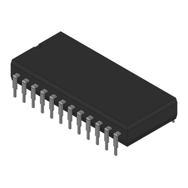
Small. 0.3". 24-Pin Plastic Package and 28-Pin PLCe
-
FUNCTIONAL
OPO
OP1
-
BLOCK DIAGRAMS
v"
v~.
rXIN
AD7341
-
OBS
OLE
S'lNCOiJT { J
GENERAL DESCRIPTION
The AD7341 and AD7371 are reconstruction and antialiasing
fLltersdesigned for use in high speed voiceband modems with
speeds up to 14.4 kbitslsec) in accordance with CCITT V.32
and V.33 recommendations. These Hlters, along with the
AD7840 DAC) the AD7871 ADC and a digital signal processor
(DSP) can be used to implement a complete modern.
01'0
OP1
The AD7341 is the transmit or reconstruction ftlter. It implements the filter function using a seventh order low pass
switched capacitor filter and a second order low pass continuous
time filter. The cutoff frequency is 305kHz.
The AD7371 is the receive fIlter. It is a high order bandpass
fLlterwith a lower cUtoff frequency of 180Hz and an upper
cutoff frequency of 3.5kHz. The ftlter function is implemented
using a second order low pass continuous time fIlter, a fourth
order high pass switched capacitor fIlter and a seventh order low
pass switched capacitor fIlter.
TE
Vco
Va.
RXIN
SVNCOUT (3
AD7371
oso OS; OS2
REV. A
Information furnished by Analog Devices is believed to be accurate and
reliable. However, no responsibility is assumed by Analog Devices for its
use, nor for any infringements of patents or other rights of third parties
which may result from its use. No license is granted by implicationor
otherwise under any patent or patent rights of Analog Devices.
One Technology Way, P,O. Box 9106, Norwood, MA 02062-9106
Tel: 617/329-4700
Fax: 617/326-8703
Twx; 710/394-6577
West Coast
Central
Atlantic
714/641-9391
214/231-5094
215/643-7790
�- Page
ANALOG DEVICES fAX-ON-DEHAND HOTLINE
29
AD7341/AD7371-SPECIFICATIONS
-'
=
=
=
= Vee 5V ::f:5%; Vss -5V ::f: 5%; AGND DGND= OV;ClKIN= 288kHz(MIS Ratio
set at OdB,unlessotherwise
stated,)
60/40. TA +25DC. Attenuator
1 (VDD
FILJER
TRANSMIT
=
.-..--.
AD734lJN
AD7341JP
Parameter
Units
INPUT CHARACTERISTICS
:t3
Input Signal Range
100
Input Impedance
FILTER CHARACTERISTICSz, 3 ,
i 288
CLKIN Frequency
3.5
Cutoff Frequency
-80
Second Harmonic
-80
Third and Higher Harmonics
0.4
Passband Ripple
:to.5
Passband Gain Error
Stopband Rejection
Differential Group Delay
OUTPUT CHARACTERISTICS
Output Voltage
Offset: Voltage
Attenuation Range
Relative Accuracr' 4
Output Resistance
LOGIC INPUTS
WR, DB2-DB7, DPO, DPl,
DS(}-DS2, SYNCIN, CLKIN
VINH, Input High Voltage
VINL' Input Low Voltage
IINH' Input Current
CJN, Input Capacitance
CLKIN Divider Range (Nl)5
72
75
70
70
350
:!:3
:t70
0 to -38
:!:O.l
0.2
2.0
0.8
10
10
1 to 4
kHz
kHz
dB typ
dB typ
dB Max
dB max
dB min
dB typ
dB typ
dB mm
fLstyp
VDD
Vec
Vss
IDD
+ Ice
Iss
Power Dissipation
I to 8
fcLKIN/(NIX5xN2)
lIfa.KtN
2.4
0.4
4.75/5.25
4.7515.25
-4.751-5.25
25
25
265
Test Conditions/Comments
Nl = 1 (i.e., DPO= 1, DPl =0)
O.ldB Down from the Lowest Point in the Passband
O:5fs3.3kHz
Deviation from Nominal Setting on Programmable
; Attenuator
0:5fs3.5kHz
SNR Includes Noise and Harmonics
Attenuator
Set at
- 3OdB,
O:5f:53.5kHz
f~6.lkHz
0:5fs3.3kHz and Referenced to the AbsolUte
Group Delay at 1kHz
OLE
Vmax
mV max
dB
dBtyp
n typ
RL = 3kfl, CL = lOOpF
Determined by DB2-DB7, See Table III
TE
Vmin
Vmax
I-LAmax
pF Max
CLKIN Can Be Set to 288kHz, 576kHz, 864kHz or
1.152MHz. NI Is Set by DPO, DPl.
LOGIC OUTPUTS SYNCOUr
Divider Range (N2)
Frequency
Pulse Width
VOH' Output High Voltage
VOL' Output Low Voltage
POWER SUPPLIES
--
Vmax
Mn typ
OBS
Signal-to-Noise Ratio
= 40/60to
N2 Is Set by DS(}-DS2.
kHz
fLS
Vmm
Vmax
IsOURCE
= 4OOfLA
IS1NK=--1.6mA
V min/V roax
V minN max
V minN max
mA Max
IDAMax
roW max
NOTES
.
IOperating temperatUre ranges as follows: J versions: 0 to + 70.C.
zSpedfied fur an input frequency of 288kHz. This is internally divided by 5 to produce a switched capacitor filter frequency of 57. 6kHz. For input &equencies
lower than 288kHz, the filter response is shifted down by the ratio of this input frequency to 288kHz.
'Measured using a :r3V, 1kHz sine wave.
'Measured over the full attenuation range.
~Required to derive internal frequency of 288kHz from CLKIN.
6Detennined by data transmission rate.
Spedfications
subj~t
to change without notice.
-2-
REV. A
�- Page
ANALOG DEVICES fAX-ON-DEMAND HOTLINE
'
'
RECEIVEFIL JER
o
30
AD7341/AD7371
= Vee= 5V:t: 5%; Vss= -5V :!:: 5%;AGND= DGND
= OV;CLKIN= 288kHzMISRatio= 40/60to
60/40.TA = +25°C.PGAsetat OdD,unlessotherwise
stated.)
(VOII
,...,
AD7371JN
AD7371JP
Parameter
Units
Test Conditions/Comments
"
INPUT CHARACTERISTICS
Input Signal Range
Input Impedance
::':3
10
""
FILTER
CHARACTERISTICS2,
,
.
3
CLKIN Frequency
Lower Cutoff Frequency
Upper Cutoff Frequency
Second Harmonic
Third and Higher Harmonics
Passband Ripple
Passband Gain Error
Signal-to-Noise Ratio
288
180
3.5
80
-80
0.4
:to.S
72
75
60
66
40
360
OBS
Stopband Rejection
Differential Group Delay
OUTPUT CHARACTERISTICS
Output Voltage
Offset Voltage
Gain Range
Relative Accuracy3, 4
Output Resistance
:t3
::':70
0 to +24
:to.1
0.2
LOGIC INPUTS
WR, DBO-DB7,DPO,DPl,
2.0
VINl.>Input Low Voltage
lINn, Input Current
0.8
10
CIN' Input Capacitance
CLKIN Divider Range (NI)s
LOGIC OUTPUTS SYNCOUT
Divider Range (N2)
Frequency
Pulse Width
V on, Output High Voltage
VOL> Output Low Voltage
kHz
Hz
kHz
dB typ
dB typ
dB max
dB max
dB min
dB typ
dB typ
dB min
dB typ
fLSryp
NI=! (i.e., DPO=I, DPl=O)
O.ldB Down from the Lowest Point in the Passband
O.ldB Down from the Lowest Point in the Passband
200Hzsf:-s3.3kHz
DeviatIon from Nominal Setnng on PGA
180Hz:-Sf:-S3.5kHz
InpUt Signal Level of -24dB; PGA Gain Set at +24dB
f6.1kHz
f60kHz
SOOHzsfs3.3kHz and Referenced to the AbsolUte
Group Delay at 1kHz
OLE
Vmax
mV max
dB
10
1 to 4
Determined
Vmin
Vmax
fLAmax
I
I
i
pF max
II
4.75/5.25
4.75/5.25
-4.75/-5.25
25
25
265
VDD
Vc.c
Vss
Inn + Ice
Is5
Power Dissipation
non
CLKIN Can Be Set to 288kHz, 576kHz, 864kHzor
i
---
N2 Is Set by DSO-DS2.
;
fLS
i
V min
Vmax
!
IsouRcE=400fLA
'
ISINK
SUPPLIES
see Table VI
I 1.152MHz. Nl Is Set by DPO, DP1.
1 to 8
kHz
TE
by DBO-DB7,
dB typ
!1 typ
--
fCLKIN/eNI xSxN2)
l/fcLKIN
2.4
0.4
-".'..",
RI,. = 3k!1, Cl. = 100pF
I!
DSO-DS2, SYNCIN, CLKIN
VINH' Input High Voltage
POWER
V max
kD typ
= 1.6mA
mm'.m-
V minIV rnax
V minIV max
V minN max
mA max
mA max
mW max
NOTES
'Operating
temperature
ranges as follows: J versions: '0 to +70'C.
'Specified for an input frequency of 288kHz. This is inrernaJly divided by 5 to produce a swirched capacitor tjltc:r frequency of 57.6kHz. For inpUt frequencies
lower than 288kHz, the filter response is shifted down by the ratio of this input frequency to 288kHz.
'Measured using a :t3V, 1kHz sine wave.
'Measured over the full attenuation range.
'Required to derive a switched capacimr filter frequency of 288kHz from CLKIN.
'Determined by dara transmission rate.
Specifications subject to change without notice.
REV. A
-3-
�ANALOG DEVICES fAX-ON-DEMAND HOTLINE
-
Pag!!
31
AD7341/AD7371
TIMINGCHARACTERISTICS1
(VDD
=
Vee
= +5V
%5%.
Vss
= -5V
1
%5%)
080..087
Parameter
Limit at
TA
+2S0C
Umts
Comments
tWR
80
ns min
Write Pulse Width
60
20
80
ns min
ns min
ns min
Data Setup Time
Data Hold Time
SYNCIN Pulse Width
tDS
tDH
tSYNCJN
=
1
I
a.
1
WR
""'"
Operating Temperature Range
JVersions
t-
.;--=.:
5V
:~//////~
..
ov
I
I
I
I
I
I
r
'\.
I
5V
OV
NOTES
,. ALL INPUT SIGNAL RISE AND FAll
of +5V 1'~t1~20~..
2. TIMING MEASUREMENT
TIMES MEASURED FROM 10%
10
90%
REFERENCE LEVEL IS IV," . V~112
Figure 1. AD7341/AD7371
ABSOLUTE MAXIMUM RATINGS.
VootoAGND
:..-O.3Vto+7V
VcctoDGND
O.3Vto+7V
VDDtoVcc
O.6Vto+O.6V
VsstoDGND
+O.3Vto-7V
AGNDtoDGND
O.3VtoVcc
RXIN, TXIN to AGND
Vss -O.3V to VDD + O.3V
RXOUT, TXOUT to AGNDt ...Vss-O.3V to VDD + O.3V
Digital Input Voltage to DGND . . . . . . -O.3V to Vcc + O.3V
Power Dissipation(Any Package)to +75°C
DATA VAUO
:/,///////.J(
NOTE
'Timing specifications are sample tested at +2S.C to ensure compliance. All
input control signals are specified with tR = t,,= lOns (10% to 90% of +SV)
and timed from a voltage level of + 1.6V.
Specifications subject to change without notice.
OBS
: 10"I
10.
a.
1
I
Timing Diagram
StorageTemperature Range. . . . . . . . . . . -65°C to + 150°C
Lead Temperature (Soldering,IOsecs)
+300°C
OLE
NOTE
'RXOUT, TXOUT may be shorted to AGND, DGND, VDD, Vcc> Vss
provided that the power dissipation of the package is not exceeded.
lOOOmW
Oto+70°C
*Stresses above those listed under "Absolute Maximum Ratings" may cause
permanent damage to the device. This is a stress rating only and functional
operation of the device at these or any other conditions above those indicated in the operational sections of this specification is not implied. Exposure to absolute maximum rating conditions for extended periods of time
may affect device reliability. Only one absolute maximum rating may be
applied at anyone time.
CAUTION
ESD (electrostatic discharge) sensitive device. The digital control inputs are diode protected;
however, permanent damage may occur on unconnected devices subject to high energy electrostatic fields. Unused devices must be stored in conductive foam or shunts. The protective foam
should be discharged to the destination socket before devices are removed.
TE
ORDERING GUIDE
Model
Function
AD734lJN
AD734lJP
AD737lJN
AD7371JP
Transmit Filter
Transmit Filter
Receive Filter
Receive Filter
*N
= Plastic DIP; P = Plastic
I
;
Temperature
Range
DoCto +700e
ooe to + 70ce
DoCto +70ce
Doe to + 70oe
i
Package
Option*
N-24
P-28A
N-24
P-28A
Leaded Chip Carrier (PLCC).
-4-
REV. A
�ANALOG DEVICES fAX-ON-DEMAND HOTLINE
- Page
3c
AD7341/AD7371
PIN CONFIGURATIONS
DIP
PLCC
241TXlN
TXOUT11 I .
Z
~..>-
.. 5
z
~
: ><
I>'" :>
'" "
Z
Q
0 " '"
~ i uz
:> ".. Z
.. :>
'"
2>
MEaUENCY..
I
I
j
i
I
-.-
150
-700
3.3k
Hz
Figure 6. Passband Ripple in the
AD7341/AD7371
!
-700
i
I
j
i I I
",,"-.."..
!
!
I
>- -300
-600
-
;.
~
w
'"
~
-400
0
"'"
-SOD
;
-500
80
!
!
!
i
..zoo
-
FREQUENCY
,
'"
"
i
SOD
!
j


 工商网监
湘ICP备2023018690号
工商网监
湘ICP备2023018690号
