14-Bit, 2400 MSPS RF DAC
with 4-Channel Signal Processing
AD9789
Data Sheet
The on-chip rate converter supports a wide range of baud rates
with a fixed DAC clock. The digital upconverter can place the
channels from 0 to 0.5 × fDAC. This permits four contiguous
channels to be synthesized and placed anywhere from dc to fDAC.
FEATURES
DOCSIS 3.0 performance: 4 QAM carriers
ACLR over full band (47 MHz to 1 GHz)
−75 dBc @ fOUT = 200 MHz
−72 dBc @ fOUT = 800 MHz (noise)
−67 dBc @ fOUT = 800 MHz (harmonics)
Unequalized MER = 42 dB
On chip and bypassable
4 QAM encoders with SRRC filters, 16× to 512× interpolation,
rate converters, and modulators
Flexible data interface: 4, 8, 16, or 32 bits wide with parity
Power: 1.6 W (IFS = 20 mA, fDAC = 2.4 GHz, LVDS interface)
Direct to RF synthesis support with fS mix mode
Built-in self-test (BIST) support
Input connectivity check
Internal random number generator
The AD9789 includes a serial peripheral interface (SPI) for
device configuration and status register readback. The flexible
digital interface can be configured for data bus widths of 4, 8,
16, and 32 bits. It can accept real or complex data.
The AD9789 operates from 1.5 V, 1.8 V, and 3.3 V supplies for
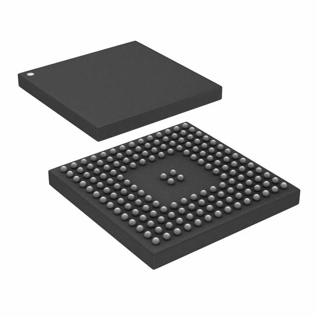
a total power consumption of 1.6 W. It is supplied in a 164-ball
chip scale package ball grid array for lower thermal impedance
and reduced package parasitics. No special power sequencing
is required. The clock receiver powers up muted to prevent
start-up noise.
PRODUCT HIGHLIGHTS
APPLICATIONS
1.
Broadband communications systems
CMTS/DVB
Cellular infrastructure
Point-to-point wireless
2.
3.
GENERAL DESCRIPTION
4.
The AD9789 is a flexible QAM encoder/interpolator/upconverter
combined with a high performance, 2400 MSPS, 14-bit RF digitalto-analog converter (DAC). The flexible digital interface can
accept up to four channels of complex data. The QAM encoder
supports constellation sizes of 16, 32, 64, 128, and 256 with
SRRC filter coefficients for all standards.
5.
Highly integrated and configurable QAM mappers, interpolators, and upconverters for direct synthesis of one to
four DOCSIS- or DVB-C-compatible channels in a block.
Low noise and intermodulation distortion (IMD) performance enable high quality synthesis of signals up to 1 GHz.
Flexible data interface supports LVDS for improved SFDR
or CMOS input data for less demanding applications.
Interface is configurable from 4-bit nibbles to 32-bit words
and can run at up to 150 MHz CMOS or 150 MHz LVDS
double data rate (DDR).
Manufactured on a CMOS process, the AD9789 uses a
proprietary switching technique that enhances dynamic
performance.
FUNCTIONAL BLOCK DIAGRAM
DCO
FS
RETIMER
DATA FORMATTER/
ASSEMBLER
150MHz
LVDS/CMOS
CMOS
16 TO 31
LVDS
FALL
DATA
QAM/
FILTER/
NCO
DATA
QAM/
FILTER/
NCO
DATA
QAM/
FILTER/
NCO
DATA
QAM/
FILTER/
NCO
16×
INTERPOLATOR
AND BPF
+ SCALARS
14-BIT
2.4GSPS
DAC
SPI
IRQ
RS
07852-001
32 INPUT
PINS
AND
2 PARITY
PINS
CMOS
0 TO 15
LVDS
RISE
Figure 1.
Rev. B
Document Feedback
Information furnished by Analog Devices is believed to be accurate and reliable. However, no
responsibility is assumed by Analog Devices for its use, nor for any infringements of patents or other
rights of third parties that may result from its use. Specifications subject to change without notice. No
license is granted by implication or otherwise under any patent or patent rights of Analog Devices.
Trademarks and registered trademarks are the property of their respective owners.
One Technology Way, P.O. Box 9106, Norwood, MA 02062-9106, U.S.A.
Tel: 781.329.4700
©2009-2019 Analog Devices, Inc. All rights reserved.
Technical Support
www.analog.com
�AD9789
Data Sheet
TABLE OF CONTENTS
Features .............................................................................................. 1
SPI Register Descriptions .......................................................... 29
Applications ....................................................................................... 1
Theory of Operation ...................................................................... 39
General Description ......................................................................... 1
Datapath Signal Processing ....................................................... 39
Product Highlights ........................................................................... 1
Digital Block Upconverter ........................................................ 43
Functional Block Diagram .............................................................. 1
Digital Interface Modes ............................................................. 45
Revision History ............................................................................... 2
Analog Modes of Operation ..................................................... 54
Detailed Functional Block Diagrams ............................................. 3
Analog Control Registers .......................................................... 55
Specifications..................................................................................... 4
Voltage Reference ....................................................................... 56
DC Specifications ......................................................................... 4
DAC Output Stages .................................................................... 56
Digital Specifications ................................................................... 5
Clocking the AD9789 ................................................................ 57
AC Specifications.......................................................................... 6
Mu Delay Controller .................................................................. 58
Absolute Maximum Ratings............................................................ 8
Interrupt Requests ...................................................................... 61
Thermal Resistance ...................................................................... 8
Recommended Start-Up Sequence .......................................... 62
ESD Caution .................................................................................. 8
Customer BIST Modes ................................................................... 63
Pin Configurations and Function Descriptions ........................... 9
Using the Internal PRN Generator to Test QAM Output AC
Performance ................................................................................ 63
Typical Performance Characteristics ........................................... 12
Terminology .................................................................................... 22
Serial Control Port.......................................................................... 23
Serial Control Port Pin Descriptions ....................................... 23
General Operation of Serial Control Port ............................... 23
Instruction Word (16 Bits) ........................................................ 24
MSB/LSB First Transfers............................................................ 24
Using the Internal Built-In Self-Test (BIST) to Test for Digital
Data Input Connectivity ............................................................. 63
QAM Constellation Maps ............................................................. 65
Channelizer Mode Pin Mapping for CMOS and LVDS ............ 68
Outline Dimensions ....................................................................... 74
Ordering Guide .......................................................................... 74
SPI Register Map............................................................................. 27
REVISION HISTORY
4/2019—Rev. A to Rev. B
Change to General Description Section ........................................ 1
Change to Digital 16x Tunable Band-Pass Filter Section .......... 44
Change to Retimer Operation Section ........................................ 49
Change to Endnote 1, Table 79 ..................................................... 62
7/2011—Rev. 0 to Rev. A
Change: DVB to DVB-C ............................................... Throughout
Changes to Table 2, DAC Clock Input (CLKP, CLKN): Added
DAC Clock Rate Parameter ............................................................. 5
Changes to Table 3, Dynamic Performance, DAC Update Rate
Parameter; Added Adjusted DAC Update Rate Parameter .........6
Changes to Captions for Figure 42, Figure 44, Figure 46,
Figure 49 .......................................................................................... 18
Changes to Digital 16x Tunable Band-Pass Filter Section, Third
Paragraph ......................................................................................... 44
Changes to Retimer and Latency Look-Up Tables Section,
Second Paragraph ........................................................................... 50
Changes to Captions for Figure 122, Figure 124, Figure 125 ... 65
4/2009—Revision 0: Initial Version
Rev. B | Page 2 of 76
�Data Sheet
AD9789
DETAILED FUNCTIONAL BLOCK DIAGRAMS
32 INPUT
PINS
4 TO
RETIMER 32 BITS
LVDS/CMOS
CMOS
16 TO 31
LVDS
FALL
DATA FORMATTER/
ASSEMBLER
DATAPATH
0
UP TO
32 BITS
DATAPATH
1
UP TO
32 BITS
P0
P1
FS
DCO
UP TO
32 BITS
UP TO
32 BITS
CLK
CTL
DATAPATH
2
16×
INTERPOLATOR
BPF
fC = 0 TO
fDAC/2
SUM
SCALE
BPF
DATAPATH
3
fC
Figure 2. Digital Signal Processing Functional Block Diagram
24-BIT NCO
0 TO fDAC /16
QAM
MAPPER
SRRC
2N
(N = 0 TO 5)
INPUT
SCALE
BYPASS
QAM
BYPASS
SRRC
RATE
CONVERTER
P/Q 24-BIT
(P/Q = 0.5 TO 1)
CH GAIN
0× TO 2×
Figure 3. Channel 0 Through Channel 3 Datapath Block Detail (I and Q Paths Are Identical So Only One Is Shown)
Rev. B | Page 3 of 76
07852-003
2
07852-002
CMOS
0 TO 15
LVDS
RISE
�AD9789
Data Sheet
SPECIFICATIONS
DC SPECIFICATIONS
AVDD33 = DVDD33 = 3.3 V, CVDD18 = DVDD18 = 1.8 V, DVDD15 = 1.5 V, fDAC = 2.4 GHz, IFS = 20 mA, unless otherwise noted.
Table 1.
Parameter
DAC RESOLUTION
ANALOG OUTPUTS
Offset Error
Gain Error (with Internal Reference)
Full-Scale Output Current (Monotonicity Guaranteed)
Output Compliance Range
Output Resistance
Output Capacitance
TEMPERATURE DRIFT
Gain
Reference Voltage
REFERENCE
Internal Reference Voltage
Output Resistance1
ANALOG SUPPLY VOLTAGES
AVDD33
CVDD18
DIGITAL SUPPLY VOLTAGES
DVDD33
DVDD18
DVDD15
SUPPLY CURRENTS AND POWER DISSIPATION
fDAC = 2.4 GSPS, fOUT = 930 MHz, IFS = 25 mA, Four Channels Enabled
IAVDD33
IDVDD18
ICVDD18
IDVDD33
CMOS Interface
LVDS Interface
IDVDD15
fDAC = 2.0 GSPS, fOUT = 70 MHz, IFS = 20 mA, CMOS Interface
IAVDD33
IDVDD18
ICVDD18
IDVDD33
IDVDD15 (Four Channels Enabled, All Signal Processing Enabled)
IDVDD15 (One Channel Enabled, 16× Interpolation Only)
Power Dissipation
fDAC = 2.4 GSPS, fOUT = 930 MHz, IFS = 25 mA, Four Channels Enabled
CMOS Interface
LVDS Interface
1
Min
8.66
−1.0
Typ
14
6.5
3.5
20.2
Max
Unit
Bits
70
1
% FSR
% FSR
mA
V
Ω
pF
135
25
ppm/°C
ppm/°C
1.2
5
V
kΩ
31.66
+1.0
3.14
1.71
3.3
1.8
3.47
1.89
V
V
3.14
1.71
1.43
3.3
1.8
1.5
3.47
1.89
1.58
V
V
V
Use an external amplifier to drive any external load.
Rev. B | Page 4 of 76
45
72
180
mA
mA
mA
42
16
640
mA
mA
mA
37.4
67.3
155.4
40.3
517
365
1.7
1.63
38.5
70.5
180
50.7
556
391
mA
mA
mA
mA
mA
mA
W
W
�Data Sheet
AD9789
DIGITAL SPECIFICATIONS
AVDD33 = DVDD33 = 3.3 V, CVDD18 = DVDD18 = 1.8 V, DVDD15 = 1.5 V, fDAC = 2.4 GHz, IFS = 20 mA, LVDS drivers and receivers
are compliant with the IEEE Std 1596.3-1996 reduced range link, unless otherwise noted.
Table 2.
Parameter
CMOS DATA INPUTS (D[31:0], P0, P1)
Input Voltage High, VIH
Input Voltage Low, VIL
Input Current High, IIH
Input Current Low, IIL
Input Capacitance
Setup Time, CMOS Data Input to CMOS_DCO1
Hold Time, CMOS Data Input to CMOS_DCO1
CMOS OUTPUTS (CMOS_FS, CMOS_DCO)
Output Voltage High, VOH
Output Voltage Low, VOL
Output Current High, IOH
Output Current Low, IOL
Maximum Clock Rate (CMOS_DCO)
CMOS_DCO to CMOS_FS Delay
LVDS DATA INPUTS (D[15:0]P, D[15:0]N, PARP, PARN)
Input Voltage Range, VIA or VIB
Input Differential Threshold, VIDTH
Input Differential Hysteresis, VIDTHH, VIDTHL
Input Differential Input Impedance, RIN
Maximum LVDS Input Rate
Setup Time, LVDS Differential Input Data to Differential DCOx2
Hold Time, LVDS Differential Input Data to Differential DCOx2
LVDS OUTPUTS (DCOP, DCON, FSP, FSN)
DCOP, FSP = VOA; DCON, FSN = VOB; 100 Ω Termination
Output Voltage High, VOA or VOB
Output Voltage Low, VOA or VOB
Output Differential Voltage, |VOD|
Output Offset Voltage, VOS
Output Impedance, Single Ended, RO
RO Mismatch Between A and B, ∆RO
Change in |VOD| Between 0 and 1, |∆VOD|
Change in VOS Between 0 and 1, ∆VOS
Output Current—Driver Shorted to Ground, ISA, ISB
Output Current—Drivers Shorted Together, ISAB
Power-Off Output Leakage, |IXA|, |IXB|
Maximum Clock Rate (DCOP, DCON)
DCOx to FSx Delay
DAC CLOCK INPUT (CLKP, CLKN)3
Differential Peak Voltage
Common-Mode Voltage
DAC Clock Rate
SERIAL PERIPHERAL INTERFACE
Maximum Clock Rate (fSCLK, 1/tSCLK)
Minimum Pulse Width High, tPWH
Minimum Pulse Width Low, tPWL
Minimum SDIO and CS to SCLK Setup, tDS
Min
Typ
2.0
3.3
0
−10
−10
Max
0.8
+10
+10
2
5.3
−1.4
2.4
0
3.3
0.4
12
12
150
0.28
0.85
825
−100
1575
+100
25
80
150
1.41
0.24
120
1375
1025
150
1150
40
200
150
0.12
1.4
Rev. B | Page 5 of 76
V
V
mA
mA
MHz
ns
mV
mV
mV
Ω
MSPS
ns
ns
0.37
2400
V
mV
MHz
250
1250
140
10
25
25
20
4
10
25
10
V
V
μA
μA
pF
ns
ns
mV
mV
mV
mV
Ω
%
mV
mV
mA
mA
mA
MHz
ns
1.8
900
20
20
Unit
MHz
ns
ns
ns
�AD9789
Data Sheet
Parameter
Minimum SCLK to SDIO Hold, tDH
Maximum SCLK to Valid SDIO and SDO, tDV
Minimum SCLK to Invalid SDIO and SDO, tDNV
INPUTS (SDIO, SCLK, CS)
Input Voltage High, VIH
Input Voltage Low, VIL
Input Current High, IIH
Input Current Low, IIL
OUTPUTS (SDO, SDIO)
Output Voltage High, VOH
Output Voltage Low, VOL
Output Current High, IOH
Output Current Low, IOL
1
2
3
Min
Typ
5
20
5
2.0
3.3
0
Max
−10
−10
0.8
+10
+10
2.4
0
3.6
0.4
Unit
ns
ns
ns
V
V
μA
μA
V
V
mA
mA
4
4
See the CMOS Interface Timing section for more information.
See the LVDS Interface Timing section for more information.
See the Clock Phase Noise Effects on AC Performance section for more information.
AC SPECIFICATIONS
AVDD33 = DVDD33 = 3.3 V, CVDD18 = DVDD18 = 1.8 V, DVDD15 = 1.5 V, fDAC = 2.4 GHz, IFS = 20 mA, digital scale = 0 dBFS, unless
otherwise noted.
Table 3.
Parameter
DYNAMIC PERFORMANCE
DAC Update Rate
Adjusted DAC Update Rate1
Output Settling Time (tST)
SPURIOUS-FREE DYNAMIC RANGE (SFDR)
fDAC = 2000 MSPS
fOUT = 100 MHz
fOUT = 316 MHz
fOUT = 550 MHz
fDAC = 2400 MSPS
fOUT = 100 MHz
fOUT = 316 MHz
fOUT = 550 MHz
fOUT = 850 MHz
TWO-TONE INTERMODULATION DISTORTION
(IMD)
fDAC = 2000 MSPS
fOUT = 100 MHz
fOUT = 316 MHz
fOUT = 550 MHz
fDAC = 2400 MSPS
fOUT = 100 MHz
fOUT = 316 MHz
fOUT = 550 MHz
fOUT = 850 MHz
NOISE SPECTRAL DENSITY (NSD)
1-Channel QAM
fOUT = 100 MHz
fOUT = 316 MHz
fOUT = 550 MHz
fOUT = 850 MHz
Test Conditions/Comments
To 0.025%
Min
Typ
Max
Unit
2400
150
13
MSPS
MSPS
ns
70
63
58
dBc
dBc
dBc
70
70
60
60
dBc
dBc
dBc
dBc
86
73
62
dBc
dBc
dBc
86
74
66
66
dBc
dBc
dBc
dBc
−167
−166.5
−166.5
−166.5
dBm/Hz
dBm/Hz
dBm/Hz
dBm/Hz
fOUT2 = fOUT1 + 1.25 MHz
fDAC = 2400 MSPS
POUT = −14.5 dBm
POUT = −15.5 dBm
POUT = −18 dBm
POUT = −18.5 dBm
Rev. B | Page 6 of 76
�Data Sheet
Parameter
ADJACENT CHANNEL LEAKAGE RATIO (ACLR)
1-Channel QAM
fOUT = 200 MHz (Harmonics)
fOUT = 200 MHz (Noise Floor)
fOUT = 500 MHz (Harmonics)
fOUT = 500 MHz (Noise Floor)
fOUT = 800 MHz (Harmonics)
fOUT = 800 MHz (Noise Floor)
2-Channel QAM
fOUT = 200 MHz (Harmonics)
fOUT = 200 MHz (Noise Floor)
fOUT = 500 MHz (Harmonics)
fOUT = 500 MHz (Noise Floor)
fOUT = 800 MHz (Harmonics)
fOUT = 800 MHz (Noise Floor)
4-Channel QAM
fOUT = 200 MHz (Harmonics)
fOUT = 200 MHz (Noise Floor)
fOUT = 500 MHz (Harmonics)
fOUT = 500 MHz (Noise Floor)
fOUT = 800 MHz (Harmonics)
fOUT = 800 MHz (Noise Floor)
WCDMA ACLR
Single Carrier
First Adjacent Channel
Second Alternate Channel
Third Alternate Channel
Single Carrier
First Adjacent Channel
Second Alternate Channel
Third Alternate Channel
Four Carrier
First Adjacent Channel
Second Alternate Channel
Third Alternate Channel
1
AD9789
Test Conditions/Comments
fDAC = 2293.76 MSPS measured in 6 MHz
channels
Min
Typ
Max
Unit
−76
−82
−74.5
−78
−69
−78
dBc
dBc
dBc
dBc
dBc
dBc
−77.5
−81
−68
−76
−66
−76
dBc
dBc
dBc
dBc
dBc
dBc
−75
−76
−69
−72
−67
−72
dBc
dBc
dBc
dBc
dBc
dBc
−70
−72.5
−74
dBc
dBc
dBc
−68
−70.4
−72.7
dBc
dBc
dBc
−63.5
−65.1
−66.9
dBc
dBc
dBc
fDAC = 2304 MSPS, mix mode second
Nyquist zone
fOUT = 1850 MHz
fOUT = 2100 MHz
fOUT = 2100 MHz
Adjusted DAC update rate is calculated as fDAC divided by the minimum required interpolation factor. For the AD9789, the minimum interpolation factor is 16. Thus,
with fDAC = 2400 MSPS, FDACadj = 2400 MSPS/16 = 150 MSPS.
Rev. B | Page 7 of 76
�AD9789
Data Sheet
ABSOLUTE MAXIMUM RATINGS
THERMAL RESISTANCE
Table 4.
Parameter
AVDD33 to AVSS
DVDD18 to DVSS
DVDD33 to DVSS
DVDD15 to DVSS
CVDD18 to AVSS
AVSS to DVSS
CLKP, CLKN to AVSS
FS, DCO to DVSS
CMOS and LVDS Data Inputs
to DVSS
IOUTN, IOUTP to AVSS
I120, VREF, IPTAT to AVSS
IRQ, CS, SCLK, SDO, SDIO, RESET
to DVSS
Junction Temperature
Storage Temperature Range
Rating
−0.3 V to +3.6 V
−0.3 V to +1.98 V
−0.3 V to +3.6 V
−0.3 V to +1.98 V
−0.3 V to +1.98 V
−0.3 V to +0.3 V
−0.3 V to CVDD18 + 0.3 V
−0.3 V to DVDD33 + 0.3 V
−0.3 V to DVDD33 + 0.3 V
θJA is specified for the worst-case conditions, that is, a device
soldered in a circuit board for surface-mount packages.
−1.0 V to AVDD33 + 0.3 V
−0.3 V to AVDD33 + 0.3 V
−0.3 V to DVDD33 + 0.3 V
ESD CAUTION
Table 5. Thermal Resistance
Package
Type
164-Ball
CSP_BGA
150°C
−65°C to +150°C
Stresses at or above those listed under Absolute Maximum
Ratings may cause permanent damage to the product. This is a
stress rating only; functional operation of the product at these
or any other conditions above those indicated in the operational
section of this specification is not implied. Operation beyond
the maximum operating conditions for extended periods may
affect product reliability.
Rev. B | Page 8 of 76
θJA
25.5
24.4
19.0
17.2
θJB
14.4
θJC
6.8
Unit
°C/W
°C/W
°C/W
°C/W
Notes
4-layer board, no vias
4-layer board, 4 PCB vias
8-layer board, 4 PCB vias
8-layer board, 16 PCB vias
�Data Sheet
AD9789
PIN CONFIGURATIONS AND FUNCTION DESCRIPTIONS
CVDD18
1
2
3
IOUTN
4
5
A
+
+
B
+
6
IOUTP
7
8
–
+
9
AVDD33
10 11
12 13 14
1
2
3
4
+
+
+
+
X
5
6
7
8
+
+
9
10 11
12 13 14
A
X
X
NC
B
+
X
X
I120
C
CLKN C
N
+
+
X
X
VREF
D
CLKP D
P
+
+
X
X
IPTAT
E
E
F
F
G
DVDD18
G
+
+
+
+
X
X
X
X
H
H
J
J
K
K
CS L
X
X
X
SB
NC
NC
L
SCLK M
CK
NC
NC
M
SDO N
DO
R
NC
NC
N
SDIO P
IO
I
NC
NC
AVSS
DVDD18
RESET
Figure 4. Clock and Analog Pins (Top View)
1
2
3
4
5
6
7
8
9
10 11
1
12 13 14
A
A
B
C
C
D
D
E
E
F
F
G
G
H
H
J
PARP
J
K
PARN
K
P1
31 27 23 19 15
11
7
M
P0
DVSS
+ DVDD15
X DVDD33
Figure 6. Digital Supply and SPI Pins (Top View)
B
L
IRQ
NC NO CONNECT
07852-006
X AVDD33
2
3
4
5
6
7
8
9
10 11
12 13 14
FSP
3
BU
CMOS_BUS
L
P+
15 13
11
9
P–
15 13
7
5
3
1
FS
FSN
6
2
CT
CMOS_CTRL
M
11
9
7
5
3
1
FS
DCOP
29 25 21 17 13
9
5
1
FS
CMOS_FS
N
14 12 10
8
6
4
2
0
DC
DCON
P
28 24 20 16 12
8
4
0
DC
CMOS_DCO
P
14 12 10
8
6
4
2
0
DC
D[31:0] CMOS DATA INPUTS
PARITY AND CONTROL INPUTS
07852-005
30 26 22 18 14 10
N
Figure 5. CMOS Mode Data Input Pins (Top View)
14 +LVDS
14 –LVDS
Figure 7. LVDS Mode Data Input Pins (Top View)
Rev. B | Page 9 of 76
07852-007
+ CVDD18
07852-004
P
�AD9789
Data Sheet
Table 6. Pin Function Descriptions
Pin No.
A1, A2, A3, A6, A9, A10, A11,
B1, B2, B3, B6, B7, B8, B9,
B10, B11, C2, C3, C6, C7, C8,
C9, C10, C11, D2, D3, D6, D7,
D8, D9, D10, D11, E1, E2, E3,
E4, E13, E14, F1, F2, F3, F4,
F11, F12, F13, F14
A4, A5, B4, B5, C4, C5, D4, D5
A7
A8
A12, A13, B12, B13, C12, C13,
D12, D13
A14
B14
C1
C14
Mnemonic
AVSS
Description
Analog Supply Ground.
CVDD18
IOUTN
IOUTP
AVDD33
1.8 V Clock Supply.
DAC Negative Output Current.
DAC Positive Output Current.
3.3 V Analog Supply.
NC
I120
CLKN
VREF
DVDD18
DVDD15
No Connect. Leave floating.
Tie this pin to analog ground with a 10 kΩ resistor to generate a 120 μA reference current.
Negative DAC Clock Input (DACCLK).
Band Gap Voltage Reference I/O. Decouple to analog ground with a 1 nF capacitor.
Output impedance is approximately 5 kΩ.
Positive DAC Clock Input (DACCLK).
Factory Test Pin. Output current, proportional to absolute temperature, is
approximately 10 μA at 25°C with a slope of approximately 20 nA/°C.
1.8 V Digital Supply.
1.5 V Digital Supply.
D1
D14
CLKP
IPTAT
E11, E12
G1, G2, G3, G4, G7, G8, G11,
G12, G13, G14
H1, H2, H3, H4, H7, H8, H11,
H12, H13, H14, J1, J2, J3, J4,
J11, J12, J13, J14
K1, K2, K3, K4, K11, K12, K13,
K14
L1
L2, L3, M2, M3, N3, N4, P3, P4
L4
L5
L6
L7
L8
L9
L10
L11
L12
L13
L14
DVSS
Digital Supply Ground.
DVDD33
3.3 V Digital Supply.
CS
NC
P1/PARP
D31/D15P
D27/D13P
D23/D11P
D19/D9P
D15/D7P
D11/D5P
D7/D3P
D3/D1P
FSP
CMOS_BUS
Active Low Chip Select for SPI.
Not Used. Leave unconnected.
CMOS/LVDS Parity Bit.
CMOS/LVDS Data Input.
CMOS/LVDS Data Input.
CMOS/LVDS Data Input.
CMOS/LVDS Data Input.
CMOS/LVDS Data Input.
CMOS/LVDS Data Input.
CMOS/LVDS Data Input.
CMOS/LVDS Data Input.
Positive LVDS Frame Sync (FSP) for Data Bus.
Active High Input. Configures data bus for CMOS inputs. Low input configures data bus
to accept LVDS inputs.
Qualifying Clock for SPI.
CMOS/LVDS Parity Bit.
CMOS/LVDS Data Input.
CMOS/LVDS Data Input.
CMOS/LVDS Data Input.
CMOS/LVDS Data Input.
CMOS/LVDS Data Input.
CMOS/LVDS Data Input.
CMOS/LVDS Data Input.
CMOS/LVDS Data Input.
Negative LVDS Frame Sync (FSN) for Data Bus.
M1
M4
M5
M6
M7
M8
M9
M10
M11
M12
M13
SCLK
P0/PARN
D30/D15N
D26/D13N
D22/D11N
D18/D9N
D14/D7N
D10/D5N
D6/D3N
D2/D1N
FSN
Rev. B | Page 10 of 76
�Data Sheet
AD9789
Pin No.
M14
Mnemonic
CMOS_CTRL
N1
N2
N5
N6
N7
N8
N9
N10
N11
N12
N13
N14
P1
P2
SDO
RESET
D29/D14P
D25/D12P
D21/D10P
D17/D8P
D13/D6P
D9/D4P
D5/D2P
D1/D0P
DCOP
CMOS_FS
SDIO
IRQ
P5
P6
P7
P8
P9
P10
P11
P12
P13
P14
D28/D14N
D24/D12N
D20/D10N
D16/D8N
D12/D6N
D8/D4N
D4/D2N
D0/D0N
DCON
CMOS_DCO
Description
Active High Input. Enables CMOS_DCO and CMOS_FS signals and disables DCOP/DCON
and FSP/FSN signals. Low input disables CMOS_DCO and CMOS_FS signals and enables
DCOP/DCON and FSP/FSN signals.
Serial Data Output for SPI.
Active High Input. Resets the AD9789.
CMOS/LVDS Data Input.
CMOS/LVDS Data Input.
CMOS/LVDS Data Input.
CMOS/LVDS Data Input.
CMOS/LVDS Data Input.
CMOS/LVDS Data Input.
CMOS/LVDS Data Input.
CMOS/LVDS Data Input.
Positive LVDS Data Clock Output (DCOP) for Data Bus.
CMOS Frame Sync for Data Bus.
Serial Data Input/Output for SPI.
Active Low, Open-Drain Interrupt Request Output. Pull up to DVDD33 with a 10 kΩ
resistor.
CMOS/LVDS Data Input.
CMOS/LVDS Data Input.
CMOS/LVDS Data Input.
CMOS/LVDS Data Input.
CMOS/LVDS Data Input.
CMOS/LVDS Data Input.
CMOS/LVDS Data Input.
CMOS/LVDS Data Input.
Negative LVDS Data Clock Output (DCON) for Data Bus.
CMOS Data Clock Output for Data Bus.
Rev. B | Page 11 of 76
�AD9789
Data Sheet
–40
–45
–45
–50
–50
–55
–55
–60
–60
SFDR (dBc)
–40
–65
–70
0
200
400
600
fOUT (MHz)
800
1000
–85
1200
–90
–45
–50
–50
HARMONIC LEVEL (dBc)
–45
–55
–60
–65
–70
–75
0dBFS
–3dBFS
–6dBFS
–12dBFS
0
200
400
600
fOUT (MHz)
800
1000
1200
1000
1200
–55
–60
–65
–70
–75
–90
0dBFS
–3dBFS
–6dBFS
–12dBFS
0
200
400
600
800
1000
1200
fOUT (MHz)
Figure 12. Third-Order Harmonic vs. fOUT over Digital Full Scale,
fDAC = 2.4 GHz, Full-Scale Current = 20 mA, Temperature = 25°C
–50
–45
–55
–50
–60
–55
–65
–60
–70
SFDR (dBc)
–40
–65
–70
–75
–75
–80
–85
32mA
20mA
8mA
–80
–85
0
200
400
600
800
1000
+85°C
+25°C
–40°C
–90
–95
1200
fOUT (MHz)
07852-011
SFDR (dBc)
800
–85
Figure 9. Second-Order Harmonic vs. fOUT over Digital Full Scale,
fDAC = 2.4 GHz, Full-Scale Current = 20 mA, Temperature = 25°C
–90
600
–80
07852-009
HARMONIC LEVEL (dBc)
–40
–90
400
Figure 11. SFDR vs. fOUT over Digital Full Scale, fDAC = 2.4 GHz,
Full-Scale Current = 20 mA, Temperature = 25°C
–40
–85
200
fOUT (MHz)
Figure 8. SFDR vs. fOUT over fDAC, Full-Scale Current = 20 mA,
Digital Scale = 0 dBFS, Temperature = 25°C
–80
0
Figure 10. SFDR vs. fOUT over Full-Scale Current, fDAC = 2.4 GHz,
Digital Scale = 0 dBFS, Temperature = 25°C
–100
0
200
400
600
800
1000
1200
fOUT (MHz)
Figure 13. SFDR vs. fOUT over Temperature, fDAC = 2.4 GHz,
Full-Scale Current = 20 mA, Digital Scale = 0 dBFS
Rev. B | Page 12 of 76
07852-008
–90
0dBFS
–3dBFS
–6dBFS
–12dBFS
–80
07852-010
–85
–70
–75
2.4GHz
2.2GHz
2GHz
1.6GHz
1GHz
–80
–65
07852-012
–75
07852-013
SFDR (dBc)
TYPICAL PERFORMANCE CHARACTERISTICS
�Data Sheet
AD9789
90
100
80
90
80
70
IMD (dBc)
60
50
0
100
200
300
400
500
600 700
fOUT (MHz)
800
900 1000 1100
30
100
90
90
80
200
300
400
500
600
700
800
900 1000 1100
70
70
IMD (dBc)
60
60
50
50
32mA
20mA
8mA
0
100
200
300
400
500
600 700
fOUT (MHz)
800
+85°C
+25°C
–40°C
40
900 1000 1100
30
07852-038
40
0
200
300
400
500
600
700
800
900 1000 1100
fOUT (MHz)
Figure 18. Third-Order IMD vs. fOUT over Temperature, fDAC = 2.4 GHz,
Full-Scale Current = 20 mA, Digital Scale = 0 dBFS
Figure 15. Third-Order IMD vs. fOUT over Full-Scale Current, fDAC = 2.4 GHz,
Digital Scale = 0 dBFS, Temperature = 25°C
–155
–157
–157
–159
–159
–161
–161
NSD (dBm/Hz)
–155
–163
–165
–167
–169
–163
–165
–167
–169
2.4GHz
2.0GHz
1.6GHz
–173
0
200
400
600
fOUT (MHz)
800
1000
+85°C
+25°C
–40°C
–171
–173
1200
–175
07852-016
–171
–175
100
07852-041
IMD (dBc)
100
Figure 17. Third-Order IMD vs. fOUT over Digital Full Scale, fDAC = 2.4 GHz,
Full-Scale Current = 20 mA, Temperature = 25°C
80
NSD (dBm/Hz)
0
fOUT (MHz)
Figure 14. Third-Order IMD vs. fOUT over fDAC, Full-Scale Current = 20 mA,
Digital Scale = 0 dBFS, Temperature = 25°C
30
0dBFS
–3dBFS
–6dBFS
–12dBFS
40
07852-034
40
30
50
2.4GHz
2.0GHz
1.6GHz
1.0GHz
07852-037
60
Figure 16. NSD vs. fOUT over fDAC, 1-Channel QAM, Full-Scale Current = 20 mA
0
200
400
600
fOUT (MHz)
800
1000
1200
07852-019
IMD (dBc)
70
Figure 19. NSD vs. fOUT over Temperature, 1-Channel QAM, fDAC = 2.4 GHz,
Full-Scale Current = 20 mA
Rev. B | Page 13 of 76
�AD9789
Data Sheet
–5
DOCSIS3
–40°C
0°C
+25°C
+85°C
ACLR (dBc)
–25
–35
–45
–45
–55
–65
–65
–75
–75
–85
50
250
450
650
FREQUENCY (MHz)
850
–85
50
Figure 20. ACLR Performance over Temperature, 1-Channel QAM,
fDAC = 2.3 GHz, Full-Scale Current = 20 mA, fOUT = 200 MHz, Sum Scale = 48
(DOCSIS SPEC Is −73 dBc; Harmonic Exception Is −63 dBc)
–55
–60
–60
HARMONIC LEVEL (dBc)
–55
–65
–70
–75
DOCSIS3
25°C
65°C
85°C
–80
–85
0
100
200
300
400
500 600
fOUT (MHz)
700
800
900
250
350
450 550
650
FREQUENCY (MHz)
750
1000
850
950
–65
–70
–75
DOCSIS3
25°C
65°C
85°C
–80
Figure 21. Second-Order Harmonic Performance vs. fOUT over Temperature,
1-Channel QAM, fDAC = 2.3 GHz, Full-Scale Current = 20 mA, Sum Scale = 48
(DOCSIS SPEC Is −73 dBc; Harmonic Exception Is −63 dBc)
–85
0
100
200
300
400
500
600
700
800
900
fOUT (MHz)
1000
Figure 24. Third-Order Harmonic Performance vs. fOUT over Temperature,
1-Channel QAM, fDAC = 2.3 GHz, Full-Scale Current = 20 mA, Sum Scale = 48
(DOCSIS SPEC Is −73 dBc; Harmonic Exception Is −63 dBc)
–55
–5
DOCSIS3
25°C
65°C
85°C
–60
150
Figure 23. ACLR Performance over Temperature, 1-Channel QAM,
fDAC = 2.3 GHz, Full-Scale Current = 20 mA, fOUT = 800 MHz, Sum Scale = 48
(DOCSIS SPEC Is −73 dBc)
07852-014
HARMONIC LEVEL (dBc)
–35
–55
07852-015
ACLR (dBc)
–25
DOCSIS3
–40°C
0°C
+25°C
+85°C
–15
07852-017
–15
07852-018
–5
–15
DOCSIS3
2.3GHz
2.2GHz
2.4GHz
–25
ACLR (dBc)
ACLR (dBc)
–65
–70
–35
–45
–55
–75
–65
–80
100
200
300
400
500 600
fOUT (MHz)
700
800
900
1000
–85
50
Figure 22. Noise Floor vs. fOUT over Temperature (ACLR Measured Beyond 30 MHz),
1-Channel QAM, fDAC = 2.3 GHz, Full-Scale Current = 20 mA, Sum Scale = 48
(DOCSIS SPEC Is −73 dBc)
250
450
650
FREQUENCY (MHz)
850
1050
07852-039
0
07852-031
–85
–75
Figure 25. ACLR Performance over fDAC, 1-Channel QAM, fOUT = 850 MHz,
Full-Scale Current = 20 mA, Temperature = 25°C, Sum Scale = 48
(DOCSIS SPEC Is −73 dBc)
Rev. B | Page 14 of 76
�Data Sheet
AD9789
0
–5
DOCSIS3
CMOS
LVDS
–10
–20
DOCSIS3
25°C
65°C
85°C
–15
–25
ACLR (dBc)
–40
–50
–65
–70
100
200
300
400 500 600 700
FREQUENCY (MHz)
800
900
1000
Figure 26. ACLR Performance for CMOS and LVDS Interfaces, 1-Channel QAM,
fOUT = 840 MHz, fDAC = 2.4 GHz, Full-Scale Current = 20 mA, Sum Scale = 48
(DOCSIS SPEC Is −73 dBc)
450
650
FREQUENCY (MHz)
850
1050
Figure 29. ACLR Performance over Temperature, 2-Channel QAM,
fOUT = 200 MHz, fDAC = 2.3 GHz, Full-Scale Current = 25 mA, Sum Scale = 32
(DOCSIS SPEC Is −70 dBc; Harmonic Exception Is −63 dBc)
DOCSIS3
25°C
65°C
85°C
–60
HARMONIC LEVEL (dBc)
–25
–35
–45
–55
–65
–65
–70
–75
DOCSIS3
25°C
65°C
85°C
–80
–75
250
450
650
FREQUENCY (MHz)
850
–85
07852-042
–85
50
1050
0
100
200
300
400
500
600
700
800
900
1000
fOUT (MHz)
Figure 27. ACLR Performance over Temperature, 2-Channel QAM,
fOUT = 800 MHz, fDAC = 2.3 GHz, Full-Scale Current = 25 mA, Sum Scale = 32
(DOCSIS SPEC Is −70 dBc)
07852-045
–15
Figure 30. Second Harmonic Performance vs. fOUT over Temperature,
2-Channel QAM, fDAC = 2.3 GHz, Full-Scale Current = 25 mA, Sum Scale = 32
(DOCSIS SPEC Is −70 dBc; Harmonic Exception Is −63 dBc)
–55
–55
–60
–65
–65
ACLR (dBc)
–60
–70
–75
DOCSIS3
25°C
65°C
85°C
–70
–75
DOCSIS3
25°C
65°C
85°C
0
100
200
300
400
500
600
fOUT (MHz)
700
800
900
1000
–80
–85
07852-043
–80
–85
250
–55
–5
ACLR (dBc)
–85
50
07852-040
0
07852-044
–75
–80
HARMONIC LEVEL (dBc)
–45
–55
–60
–90
–35
Figure 28. Third-Order Harmonic Performance vs. fOUT over Temperature,
2-Channel QAM, fDAC = 2.3 GHz, Full-Scale Current = 25 mA, Sum Scale = 32
(DOCSIS SPEC Is −70 dBc; Harmonic Exception Is −63 dBc)
0
100
200
300
400
500
600
fOUT (MHz)
700
800
900
1000
07852-046
ACLR (dBc)
–30
Figure 31. Noise Floor vs. fOUT over Temperature (ACLR Measured Beyond 30 MHz),
2-Channel QAM, fDAC = 2.3 GHz, Full-Scale Current = 25 mA, Sum Scale = 32
(DOCSIS SPEC Is −70 dBc)
Rev. B | Page 15 of 76
�AD9789
Data Sheet
0
0
–10
DOCSIS3
–40°C
0°C
+25°C
+85°C
ACLR (dBc)
–40
–50
–40
–50
–60
–60
–70
–70
–80
50
250
450
650
FREQUENCY (MHz)
850
1050
–80
50
Figure 32. ACLR Performance over Temperature, 4-Channel QAM,
fOUT = 200 MHz, fDAC = 2.3 GHz, Full-Scale Current = 25 mA, Sum Scale = 20
(DOCSIS SPEC Is −67 dBc; Harmonic Exception Is −63 dBc)
–55
–60
–60
HARMONIC LEVEL (dBc)
–55
–65
–70
–75
DOCSIS3
25°C
65°C
85°C
–80
0
100
200
300
400
500 600
fOUT (MHz)
700
800
900
1000
1050
–65
–70
–75
–85
DOCSIS3
25°C
65°C
85°C
0
100
200
300
400
500
600
700
800
900
1000
fOUT (MHz)
Figure 36. Third-Order Harmonic Performance vs. fOUT over Temperature,
4-Channel QAM, fDAC = 2.3 GHz, Full-Scale Current = 25 mA, Sum Scale = 20
(DOCSIS SPEC Is −67 dBc; Harmonic Exception Is −63 dBc)
0
–55
–10
–60
–20
ACLR (dBc)
–65
ACLR (dBc)
850
–80
Figure 33. Second-Order Harmonic Performance vs. fOUT over Temperature,
4-Channel QAM, fDAC = 2.3 GHz, Full-Scale Current = 25 mA, Sum Scale = 20
(DOCSIS SPEC Is −67 dBc; Harmonic Exception Is −63 dBc)
–70
–75
100
200
300
400
500 600
fOUT (MHz)
700
800
900
1000
–30
–40
–50
–70
–80
50
07852-028
0
DOCSIS3
2.3GHz
2.2GHz
2.4GHz
–60
DOCSIS3
25°C
65°C
85°C
–80
–85
450
650
FREQUENCY (MHz)
Figure 34. Noise Floor vs. fOUT over Temperature (ACLR Measured Beyond 30 MHz),
4-Channel QAM, fDAC = 2.3 GHz, Full-Scale Current = 25 mA, Sum Scale = 20
(DOCSIS SPEC Is −67 dBc)
250
450
650
FREQUENCY (MHz)
850
1050
07852-047
–85
250
Figure 35. ACLR Performance over Temperature, 4-Channel QAM,
fOUT = 800 MHz, fDAC = 2.3 GHz, Full-Scale Current = 25 mA, Sum Scale = 20
(DOCSIS SPEC Is −67 dBc)
07852-026
HARMONIC LEVEL (dBc)
–30
07852-029
–30
DOCSIS3
–40°C
0°C
+25°C
+85°C
–20
07852-027
ACLR (dBc)
–20
07852-030
–10
Figure 37. ACLR Performance over fDAC, 4-Channel QAM, fOUT = 850 MHz,
Full-Scale Current = 25 mA, Temperature = 25°C, Sum Scale = 20
(DOCSIS SPEC Is −67 dBc)
Rev. B | Page 16 of 76
�Data Sheet
AD9789
RMS RESULTS
CARRIER POWER
–18.10dBm/
6.00000MHz
VBW 560kHz
FREQ.
OFFSET
3.375MHz
6.375MHz
12.00MHz
18.00MHz
REF BW
750.0kHz
5.250MHz
6.000MHz
6.000MHz
SPAN 42MHz
SWEEP 39.12ms (601 PTS)
LOWER
dBc
dBm
–65.57 –83.66
–75.01 –93.11
–76.83 –94.92
–77.17 –95.26
UPPER
dBc
dBm
–68.98 –87.07
–74.62 –92.71
–76.46 –94.55
–76.56 –94.66
CENTER 840.00MHz
RES BW 30kHz
Figure 38. 1-Channel QAM ACLR, fOUT = 840 MHz, Temperature = 25°C,
Sum Scale = 48, Full-Scale Current = 20 mA, Span = 42 MHz
CENTER 840.00MHz
RES BW 30kHz
RMS RESULTS
CARRIER POWER
–21.75dBm/
6.00000MHz
VBW 300kHz
FREQ.
OFFSET
3.375MHz
6.375MHz
12.00MHz
18.00MHz
REF BW
750.0kHz
5.250MHz
6.000MHz
6.000MHz
SPAN 18MHz
SWEEP 58.4ms (601 PTS)
Figure 40. 1-Channel QAM ACLR, fOUT = 840 MHz, Temperature = 25°C,
Sum Scale = 48, Full-Scale Current = 20 mA, Span = 18 MHz
REF –35.91dBm
SPAN 42MHz
SWEEP 136.2ms (601 PTS)
LOWER
UPPER
dBc
dBm
dBc
dBm
–71.64 –93.39 –72.50 –94.25
–73.71 –95.47 –66.72 –88.47
–73.58 –95.33
0.50 –21.10
–73.70 –95.45 –66.72 –88.48
VBW 300kHz
FREQ.
LOWER
UPPER
OFFSET REF BW
dBc
dBm
dBc
dBm
RMS RESULTS
CARRIER POWER 3.375MHz 750.0kHz –73.99 –91.97 –74.93 –92.91
6.375MHz 5.250MHz –74.94 –92.92 –75.35 –93.33
–17.98dBm/
6.00000MHz
ATTEN 2dB
START 831.00MHz
RES BW 30kHz
07852-061
REF –35.91dBm
ATTEN 2dB
RMS RESULTS
CARRIER POWER
–21.29dBm/
6.00000MHz
Figure 39. 2-Channel QAM ACLR, fOUT = 840 MHz, Sum Scale = 32,
Full-Scale Current = 25 mA, Span = 42 MHz, Channel 1
ATTEN 2dB
VBW 300kHz
FREQ.
OFFSET
3.375MHz
6.375MHz
12.00MHz
18.00MHz
STOP 873MHz
SWEEP 136.2ms (601 PTS)
LOWER
REF BW
dBc
dBm
750.0kHz –70.07 –92.16
5.250MHz –69.05 –90.34
6.000MHz –0.49 –21.78
6.000MHz –66.61 –87.90
UPPER
dBc
dBm
–73.20 –94.49
–73.87 –95.16
–73.29 –94.58
–73.98 –95.27
Figure 41. 2-Channel QAM ACLR, fOUT = 840 MHz, Sum Scale = 32,
Full-Scale Current = 25 mA, Span = 42 MHz, Channel 2
Rev. B | Page 17 of 76
07852-066
CENTER 840.00MHz
RES BW 56kHz
REF –32.76dBm
07852-023
ATTEN 2dB
07852-020
REF –32.76dBm
�AD9789
Data Sheet
VBW 300kHz
SPAN 18MHz
SWEEP 58.4ms (601 PTS)
FREQ.
LOWER
UPPER
OFFSET REF BW
dBc
dBm
dBc
dBm
RMS RESULTS
CARRIER POWER 3.375MHz 750.0kHz –75.37 –96.93 –75.56 –97. 11
–21.56dBm/
6.375MHz 5.250MHz –73.85 –95.41 –72.54 –94.10
6.00000MHz
CENTER 852.00MHz
RES BW 30kHz
Figure 42. Zoomed 2-Channel QAM ACLR, fOUT = 840 MHz, Sum Scale = 32,
Full-Scale Current = 25 mA, Span = 18 MHz, Channel 1
CENTER 834.00MHz
RES BW 30kHz
VBW 300kHz
RMS RESULTS
CARRIER POWER
–23.63dBm/
6.00000MHz
FREQ.
OFFSET
3.375MHz
6.375MHz
12.00MHz
18.00MHz
REF BW
750.0kHz
5.250MHz
6.000MHz
6.000MHz
SPAN 42MHz
SWEEP 136.2ms (601 PTS)
ATTEN 2dB
CENTER 852.00MHz
VBW 300kHz
RES BW 30kHz
Figure 43. 4-Channel QAM ACLR, fOUT = 840 MHz, Temperature = 25°C,
Sum Scale = 20, Full-Scale Current = 25 mA, Span = 42 MHz, Channel 1
SPAN 18MHz
SWEEP 58.4ms (601 PTS)
Figure 44. Zoomed 2-Channel QAM ACLR, fOUT = 840 MHz, Sum Scale = 32,
Full-Scale Current = 25 mA, Span = 18 MHz, Channel 2
REF –35.96dBm
LOWER
UPPER
dBc
dBm
dBc
dBm
–70.33 –93.96 –11.07 –34.70
–69.04 –92.67 –0.49 –24.12
–70.38 –94.01
0.00 –23.63
–71.02 –94.65
0.43 –23.20
VBW 300kHz
FREQ.
LOWER
UPPER
OFFSET REF BW
dBc
dBm
dBc
dBm
RMS RESULTS
CARRIER POWER 3.375MHz 750.0kHz –75.51 –96.54 –75.17 –96.20
–21.03dBm/
6.375MHz 5.250MHz –72.55 –93.58 –73.90 –94.93
6.00000MHz
ATTEN 2dB
07852-021
REF –35.96dBm
ATTEN 2dB
RMS RESULTS
CARRIER POWER
–23.23dBm/
6.00000MHz
FREQ.
OFFSET
3.375MHz
6.375MHz
12.00MHz
18.00MHz
REF BW
750.0kHz
5.250MHz
6.000MHz
6.000MHz
SPAN 42MHz
SWEEP 136.2ms (601 PTS)
LOWER
dBc
dBm
–11.10 –34.32
–0.75 –23.98
–0.59 –23.81
–0.35 –23.58
UPPER
dBc
dBm
–72.19 –95.42
–68.97 –92.20
–70.32 –93.55
–70.70 –93.93
07852-022
CENTER 840.00MHz
RES BW 30kHz
REF –35.91dBm
07852-067
ATTEN 2dB
07852-065
REF –35.91dBm
Figure 45. 4-Channel QAM ACLR, fOUT = 840 MHz, Temperature = 25°C,
Sum Scale = 20, Full-Scale Current = 25 mA, Span = 42 MHz, Channel 4
Rev. B | Page 18 of 76
�Data Sheet
AD9789
CENTER 834.00MHz
RES BW 30kHz
VBW 300kHz
REF –35.96dBm
SPAN 18MHz
SWEEP 58.4ms (601 PTS)
CENTER 852.00MHz
RES BW 30kHz
FREQ.
LOWER
UPPER
OFFSET REF BW
dBc
dBm
dBc
dBm
RMS RESULTS
CARRIER POWER 3.375MHz 750.0kHz –72.95 –96.56 –10.86 –34.48
6.375MHz 5.250MHz –69.38 –92.99 –0.51 –24.13
–23.62dBm/
6.00000MHz
Figure 49. Zoomed 4-Channel QAM ACLR, fOUT = 840 MHz, Temperature =
25°C, Sum Scale = 20, Full-Scale Current = 25 mA, Span = 18 MHz, Channel 4
50
50
48
48
46
46
44
44
42
42
40
38
38
36
+25°C
+85°C
–40°C
32
150
250
350
450
550 650
fOUT (MHz)
750
850
950
+25°C
+85°C
–40°C
34
32
30
50
07852-032
34
150
250
350
450
550
650
750
850
950
fOUT (MHz)
Figure 47. Modulation Error Ratio, Equalized, 1-Channel 256-QAM,
fDAC = 2.29376 GHz, Full-Scale Current = 20 mA, Sum Scale = 48
(Equalization Filter from Demodulation Toolbox on Spectrum Analyzer Used)
Figure 50. Modulation Error Ratio, Equalized, 4-Channel 256-QAM,
fDAC = 2.29376 GHz, Full-Scale Current = 25 mA, Sum Scale = 20
(Equalization Filter from Demodulation Toolbox on Spectrum Analyzer Used)
50
50
48
48
46
46
44
44
42
42
MER (dB)
40
38
36
40
38
36
+25°C
+85°C
–40°C
32
150
250
350
450
550 650
fOUT (MHz)
750
850
950
+25°C
+85°C
–40°C
34
32
30
50
07852-033
34
150
250
350
450
550
fOUT (MHz)
Figure 48. Modulation Error Ratio, Unequalized, 1-Channel 256-QAM,
fDAC = 2.29376 GHz, Full-Scale Current = 20 mA, Sum Scale = 48
650
750
850
950
07852-036
MER (dB)
40
07852-035
36
30
50
SPAN 18MHz
SWEEP 58.4ms (601 PTS)
VBW 300kHz
FREQ.
LOWER
UPPER
OFFSET REF BW
dBc
dBm
dBc
dBm
RMS RESULTS
CARRIER POWER 3.375MHz 750.0kHz –11.20 –34.40 –74.44 –97.64
6.375MHz 5.250MHz –0.77 –23.96 –69.07 –92.26
–23.20dBm/
6.00000MHz
MER (dB)
MER (dB)
Figure 46. Zoomed 4-Channel QAM ACLR, fOUT = 840 MHz, Temperature =
25°C, Sum Scale = 20, Full-Scale Current = 25 mA, Span = 18 MHz, Channel 1
30
50
ATTEN 2dB
07852-025
ATTEN 2dB
07852-024
REF –35.96dBm
Figure 51. Modulation Error Ratio, Unequalized, 4-Channel 256-QAM,
fDAC = 2.29376 GHz, Full-Scale Current = 25 mA, Sum Scale = 20
Rev. B | Page 19 of 76
�AD9789
Data Sheet
REF –32.62dBm
80
ATTEN 0dB
75
70
65
60
SFDR (dBc)
55
50
45
40
35
30
25
20
CENTER 2.100GHz
RES BW 30kHz
Figure 52. SFDR vs. fOUT in Mix Mode, fDAC = 2.4 GHz, Full-Scale Current = 20 mA
(Second Nyquist Zone Performance)
90
RMS RESULTS
CARRIER POWER
–19.95dBm/
3.84000MHz
85
VBW 300kHz
FREQ.
OFFSET
5.000MHz
10.00MHz
15.00MHz
20.00MHz
25.00MHz
REF BW
3.840MHz
3.840MHz
3.840MHz
3.840MHz
3.840MHz
SPAN 53.84MHz
SWEEP 174.6ms (601 PTS)
LOWER
dBc
dBm
–68.93 –88.88
–71.31 –91.26
–73.43 –93.37
–75.12 –95.07
–75.60 –95.55
UPPER
dBc
dBm
–67.99 –87.94
–70.42 –90.37
–72.68 –92.63
–74.89 –94.84
–76.51 –96.46
07852-092
10
1200 1300 1400 1500 1600 1700 1800 1900 2000 2100 2200 2300 2400
fOUT (MHz)
07852-068
15
Figure 55. One-Carrier WCDMA ACLR in Mix Mode, fOUT = 2.1 GHz,
fDAC = 2304 MHz, Full-Scale Current = 20 mA
80
75
IMD (dBc)
70
REF –38.62dBm
65
ATTEN 2dB
60
55
50
45
40
30
1200 1300 1400 1500 1600 1700 1800 1900 2000 2100 2200 2300 2400
fOUT (MHz)
07852-076
35
Figure 53. IMD vs. fOUT in Mix Mode, fDAC = 2.4 GHz, Full-Scale Current = 20 mA
(Second Nyquist Zone Performance)
–45
–50
CENTER 2.102 50GHz
RES BW 30kHz
VBW 300kHz
FIRST ADJACENT CHANNE L
SECOND ADJACENT CHANNE L
THIRD ADJACENT CHANNE L
FIFTH ADJACENT CHANNE L
RMS RESULTS
CARRIER POWER
–26.06dBm/
3.84000MHz
ACLR (dBc)
–55
–60
–65
REF BW
3.840MHz
3.840MHz
3.840MHz
3.840MHz
3.840MHz
3.840MHz
LOWER
dBc
dBm
–0.25 –26.31
–0.42 –26.48
–64.07 –90.13
–65.36 –91.42
–66.86 –92.92
–67.83 –93.89
UPPER
dBc
dBm
–0.42 –26.47
–63.50 –89.56
–65.13 –91.18
–66.97 –93.03
–68.70 –94.76
–68.64 –94.70
Figure 56. Four-Carrier WCDMA ACLR in Mix Mode, fOUT = 2.1 GHz,
fDAC = 2304 MHz, Full-Scale Current = 20 mA
–70
–75
07852-075
–80
–85
1150 1250 1350 1450 1550 1650 1750 1850 1950 2050 2150 2250
fOUT (MHz)
FREQ.
OFFSET
5.000MHz
10.00MHz
15.00MHz
20.00MHz
25.00MHz
30.00MHz
SPAN 63.84MHz
SWEEP 207ms (601 PTS)
Figure 54. ACLR vs. fOUT in Mix Mode with One-Carrier WCDMA, fDAC = 2304 MHz,
Full-Scale Current = 20 mA (Second Nyquist Zone Performance)
Rev. B | Page 20 of 76
07852-093
–40
�Data Sheet
AD9789
1100
2000
AVDD33
DVDD33 (LVDS)
DVDD33 (CMOS)
DVDD18
DVDD15
CVDD18
1600
700
600
500
400
300
1000
800
600
100
200
1.2
1.4
1.6
1.8
fDAC (GHz)
2.0
2.2
2.4
0
1.0
500
1200
POWER DISSIPATION (mW)
600
400
300
200
1.6
1.8
2.0
2.2
2.4
TOTAL (CMOS)
TOTAL (LVDS)
1000
800
600
400
200
1.2
1.4
1.6
1.8
2.0
2.2
2.4
fDAC (GHz)
0
1.0
07852-095
0
1.0
180
160
140
AVDD33
120
100
80
60
40
14
16 18 20 22 24 26
FULL-SCALE CURRENT (mA)
28
30
32
07852-098
20
12
1.6
1.8
2.0
2.2
2.4
Figure 61. Total Power Dissipation vs. fDAC, 16× Interpolation,
One Channel Enabled, fOUT = 70 MHz, Full-Scale Current = 20 mA
200
10
1.4
fDAC (GHz)
Figure 58. Power Dissipation by Supply vs. fDAC, 16× Interpolation,
One Channel Enabled, fOUT = 70 MHz, Full-Scale Current = 20 mA
8
1.2
Figure 59. AVDD33 Power Dissipation vs. Full-Scale Current
Rev. B | Page 21 of 76
07852-097
100
0
1.4
Figure 60. Total Power Dissipation vs. fDAC, 4-Channel DOCSIS, fOUT = 915 MHz,
Full-Scale Current = 25 mA (Datapath Configuration: QAM Encoder On,
SRRC Filter On, Four 2× Interpolation Filters On)
1400
AVDD33
DVDD33 (LVDS)
DVDD33 (CMOS)
DVDD18
DVDD15
CVDD18
1.2
fDAC (GHz)
700
POWER DISSIPATION (mW)
1200
400
Figure 57. Power Dissipation by Supply vs. fDAC, 4-Channel DOCSIS, fOUT = 915 MHz,
Full-Scale Current = 25 mA (Datapath Configuration: QAM Encoder On,
SRRC Filter On, Four 2× Interpolation Filters On)
POWER DISSIPATION (mW)
1400
200
0
1.0
TOTAL (CMOS)
TOTAL (LVDS)
07852-096
800
07852-094
POWER DISSIPATION (mW)
900
1800
POWER DISSIPATION (mW)
1000
�AD9789
Data Sheet
TERMINOLOGY
Monotonicity
A DAC is monotonic if the output either increases or remains
constant as the digital input increases.
Offset Error
Offset error is the deviation of the output current from the ideal
of 0. For IOUTP, 0 mA output is expected when all inputs are
set to 0. For IOUTN, 0 mA output is expected when all inputs
are set to 1.
Spurious-Free Dynamic Range (SFDR)
SFDR is the difference, in dB, between the peak amplitude of
the output signal and the peak spurious signal over the specified
bandwidth.
Noise Spectral Density (NSD)
NSD is the converter noise power per unit of bandwidth. NSD
is usually specified in dBm/Hz in the presence of a 0 dBm fullscale signal.
Gain Error
Gain error is the difference between the actual and ideal output
span. The actual span is determined by the output when all inputs
are set to 1s minus the output when all inputs are set to 0s.
Adjacent Channel Leakage Ratio (ACLR)
The adjacent channel leakage (power) ratio is the ratio, in dBc,
between the measured power within a channel relative to its
adjacent channels.
Temperature Drift
Modulation Error Ratio (MER)
Modulated signals create a discrete set of output values referred
to as a constellation. Each symbol creates an output signal corresponding to one point on the constellation. MER is a measure
of the discrepancy between the average output symbol magnitude
and the rms error magnitude of the individual symbol.
Temperature drift is specified as the maximum change from the
ambient (25°C) value to the value at either TMIN or TMAX. For offset,
gain, and reference drift, the drift is reported in ppm per °C.
Power Supply Rejection (PSR)
PSR is the maximum change in the full-scale output as the
supplies are varied from nominal to minimum and maximum
specified voltages.
Output Compliance Range
The output compliance range is the range of allowable voltage
at the output of a current output DAC. Operation beyond the
maximum compliance limits may cause either output stage
saturation or breakdown, resulting in nonlinear performance.
Intermodulation Distortion (IMD)
IMD is the result of two or more signals at different frequencies
mixing together. Many products are created according to the
formula af1 ± bf2, where a and b are integer values.
Rev. B | Page 22 of 76
�Data Sheet
AD9789
SERIAL CONTROL PORT
The AD9789 serial control port is a flexible, synchronous serial
communications port that allows an easy interface to many
industry-standard microcontrollers and microprocessors. The
AD9789 serial control port is compatible with most synchronous
transfer formats, including both the Motorola SPI® and Intel® SSR
protocols. The serial control port allows read/write access to all
registers that configure the AD9789. Single- or multiple-byte
transfers are supported, as well as MSB first or LSB first transfer
formats. The AD9789 serial control port can be configured for a
single bidirectional I/O pin (SDIO only) or for two unidirectional
I/O pins (SDIO/SDO). By default, the AD9789 is in unidirectional
long instruction mode (long instruction mode is the only
instruction mode supported).
SERIAL CONTROL PORT PIN DESCRIPTIONS
The SCLK (serial clock) pin is the serial shift clock. This pin is
an input. SCLK is used to synchronize serial control port reads
and writes. Write data bits are registered on the rising edge of
this clock, and read data bits are registered on the falling edge.
This pin is internally pulled down by a 30 kΩ resistor to ground.
SDIO (serial data input/output) is a dual-purpose pin that acts
as an input only (unidirectional mode) or as both an input and
an output (bidirectional mode). The AD9789 defaults to the
unidirectional I/O mode (Register 0x00[7] = 0).
The SDO (serial data output) pin is used only in the unidirectional
I/O mode as a separate output pin for reading back data.
CS (chip select bar) is an active low control that gates the read
and write cycles. When CS is high, SDO and SDIO are in a high
impedance state. This pin is internally pulled up by a 30 kΩ
resistor to DVDD33.
M1
CS
L1
SDO
N1
SDIO
P1
AD9789
SERIAL
CONTROL
PORT
07852-048
SCLK
Figure 62. Serial Control Port
GENERAL OPERATION OF SERIAL CONTROL PORT
A write or read operation to the AD9789 is initiated by pulling
CS low. CS stall high is supported in modes where three or
fewer bytes of data (plus the instruction data) are transferred
(see Table 7). In these modes, CS can temporarily return high
on any byte boundary, allowing time for the system controller
to process the next byte. CS can go high on byte boundaries
only and can go high during either part (instruction or data)
of the transfer.
During CS stall high mode, the serial control port state machine
enters a wait state until all data is sent. If the system controller
decides to abort the transfer before all of the data is sent, the
state machine must be reset by either completing the remaining
transfers or by returning CS low for at least one complete SCLK
cycle (but less than eight SCLK cycles). Raising CS on a nonbyte
boundary terminates the serial transfer and flushes the buffer.
In streaming mode (see Table 7), any number of data bytes can
be transferred in a continuous stream. The register address is
automatically incremented or decremented (see the MSB/LSB
First Transfers section). CS must be raised at the end of the last
byte to be transferred, thereby ending streaming mode.
Communication Cycle—Instruction Plus Data
There are two parts to a communication cycle with the AD9789.
In the first part, a 16-bit instruction word is written to the
AD9789, coincident with the first 16 SCLK rising edges. The
instruction word provides the AD9789 serial control port with
information regarding the data transfer, which is the second
part of the communication cycle. The instruction word defines
whether the upcoming data transfer is a read or a write, the
number of bytes in the data transfer, and the starting register
address for the first byte of the data transfer.
Write
If the instruction word is for a write operation, the second part
of the communication cycle is the transfer of data into the serial
control port buffer of the AD9789. Data bits are registered on
the rising edge of SCLK.
The length of the transfer (one, two, or three bytes or streaming
mode) is indicated by two bits (N1 and N0) in the instruction byte.
When the transfer is one, two, or three bytes (but not streaming
mode), CS can be raised after each sequence of eight bits to stall
the bus, except after the last byte, where it ends the cycle. When
the bus is stalled, the serial transfer resumes when CS is lowered.
Raising CS on a nonbyte boundary resets the serial control port.
During a write, streaming mode does not skip reserved or blank
registers; therefore, the user must know what bit pattern to write
to the reserved registers to preserve proper operation of the
part. It does not matter what data is written to blank registers.
Most writes to the control registers immediately reconfigure the
device. However, Register 0x16 through Register 0x1D do not
directly control device operation. They provide data to internal
logic that must perform additional operations on the data before
it is downloaded and the device configuration is changed. For
any updates to Register 0x16 through Register 0x1D to take
effect, the FREQNEW bit (Register 0x1E[7]) must be set to 1
(this bit is self-clearing). Any number of bytes of data can be
changed before updating registers. Setting the FREQNEW bit
simultaneously updates Register 0x16 through Register 0x1D.
In a similar fashion, any changes to Register 0x22 and Register
0x23 require PARMNEW (Register 0x24[7]) to be toggled from
a low state to a high state before the new values take effect.
Unlike the FREQNEW bit, PARMNEW is not self-clearing.
Rev. B | Page 23 of 76
�AD9789
Data Sheet
Read
If the instruction word is for a read operation, the next N × 8
SCLK cycles clock out the data from the address specified in the
instruction word, where N is 1 to 3 as determined by Bits[N1:N0].
If N = 4, the read operation is in streaming mode, continuing
until CS is raised. Streaming mode does not skip over reserved
or blank registers. The readback data is valid on the falling edge
of SCLK.
The default mode of the AD9789 serial control port is the unidirectional mode. In unidirectional mode, the readback data
appears on the SDO pin. It is also possible to set the AD9789 to
bidirectional mode using the SDIO_DIR bit (Register 0x00[7]).
In bidirectional mode, both the sent data and the readback data
appear on the SDIO pin.
A readback request reads the data that is in the serial control port
buffer area or the data in the active registers (see Figure 63).
The AD9789 supports only the long instruction mode; therefore,
Register 0x00[4:3] reads 11 (this register uses mirrored bits).
Long instruction mode is the default at power-up or reset, and
writing to these bits has no effect.
SDO
CS
SERIAL
CONTROL
PORT
FREQNEW
WRITE REGISTER 0x1E = 0x10
TO UPDATE REGISTERS
07852-049
SDIO
ACTIVE REGISTERS
SCLK
BUFFER REGISTERS
The AD9789 uses Register Address 0x00 to Register Address 0x55.
Figure 63. Relationship Between Serial Control Port Buffer Registers and
Active Registers of the AD9789
INSTRUCTION WORD (16 BITS)
The MSB of the instruction word is R/W, which indicates
whether the instruction is a read or a write. The next two bits,
N1 and N0, indicate the length of the transfer in bytes. The final
13 bits (Bits[A12:A0]) are the address at which to begin the read
or write operation.
For a write, the instruction word is followed by the number of
bytes of data indicated by Bits[N1:N0] (see Table 7).
Table 7. Byte Transfer Count
N1
0
0
1
1
N0
0
1
0
1
Bytes to Transfer
1
2
3
Streaming mode
Bits[A12:A0] select the address within the register map that is
written to or read from during the data transfer portion of the
communication cycle. Only Bits[A6:A0] are needed to cover the
range of the 0x55 registers used by the AD9789. Bits[A12:A7]
must always be 0. For multibyte transfers, this address is the
starting byte address. In MSB first mode, subsequent bytes
increment the address.
MSB/LSB FIRST TRANSFERS
The AD9789 instruction word and byte data can be MSB first or
LSB first. Any data written to Register 0x00 must be mirrored,
the upper four bits (Bits[7:4]) with the lower four bits (Bits [3:0]).
This makes it irrelevant whether LSB first or MSB first is in
effect. As an example of this mirroring, the default setting for
Register 0x00[7:0] is 0x18, which mirrors Bit 4 and Bit 3. These
bits set the long instruction mode (the default and the only
mode supported). The default for the AD9789 is MSB first.
When LSB first is set by Register 0x00[1] and Register 0x00[6],
it takes effect immediately. In multibyte transfers, subsequent
bytes reflect any changes in the serial port configuration.
When MSB first mode is active, the instruction and data bytes
must be written from MSB to LSB. Multibyte data transfers in
MSB first format start with an instruction byte that includes the
register address of the most significant data byte. Subsequent
data bytes must follow in order from the high address to the low
address. In MSB first mode, the serial control port internal
address generator decrements for each data byte of the multibyte transfer cycle.
When LSB first mode is active, the instruction and data bytes
must be written from LSB to MSB. Multibyte data transfers in
LSB first format start with an instruction byte that includes the
register address of the least significant data byte followed by
multiple data bytes. The internal byte address generator of the
serial control port increments for each byte of the multibyte
transfer cycle.
The AD9789 serial control port register address decrements
from the register address just written toward 0x00 for multibyte
I/O operations if the MSB first mode is active (default). If the
LSB first mode is active, the register address of the serial control
port increments from the address just written toward 0x55 for
multibyte I/O operations.
Streaming mode always terminates when it reaches Address 0x2F.
Note that unused addresses are not skipped during multibyte I/O
operations.
Table 8. Streaming Mode (No Addresses Are Skipped)
Write Mode
LSB First
MSB First
Rev. B | Page 24 of 76
Address Direction
Increment
Decrement
Stop Sequence
0x02D, 0x02E, 0x02F, stop
0x001, 0x000, 0x02F, stop
�Data Sheet
AD9789
Table 9. Serial Control Port, 16-Bit Instruction Word, MSB First
MSB
I15
I14
I13
I12
I11
I10
I9
I8
I7
I6
I5
I4
I3
I2
I1
LSB
I0
R/W
N1
N0
A12
A11
A10
A9
A8
A7
A6
A5
A4
A3
A2
A1
A0
CS
SCLK DON'T CARE
SDIO DON'T CARE
R/W N1 N0 A12 A11 A10 A9 A8 A7 A6 A5 A4 A3 A2 A1 A0
D7 D6 D5 D4 D3 D2 D1 D0 D7 D6 D5 D4 D3 D2 D1 D0
16-BIT INSTRUCTION HEADER
REGISTER (N) DATA
DON'T CARE
REGISTER (N – 1) DATA
07852-050
DON'T CARE
Figure 64. Serial Control Port Write—MSB First, 16-Bit Instruction, Two Bytes of Data
CS
SCLK
DON'T CARE
SDIO
DON'T CARE
D7 D6 D5 D4 D3 D2 D1 D0 D7 D6 D5 D4 D3 D2 D1 D0 D7 D6 D5 D4 D3 D2 D1 D0 D7 D6 D5 D4 D3 D2 D1 D0
16-BIT INSTRUCTION HEADER
REGISTER (N) DATA
REGISTER (N – 1) DATA REGISTER (N – 2) DATA
REGISTER (N – 3) DATA
DON'T
CARE
07852-051
SDO
DON'T CARE
R/W N1 N0 A12 A11 A10 A9 A8 A7 A6 A5 A4 A3 A2 A1 A0
Figure 65. Serial Control Port Read—MSB First, 16-Bit Instruction, Four Bytes of Data
tDS
tHI
tS
tDH
CS
DON'T CARE
SDIO
DON'T CARE
DON'T CARE
N1
R/W
N0
A12
A11
A10
A9
A8
A7
A6
A5
D4
D3
D2
D1
D0
DON'T CARE
07852-052
SCLK
tC
tCLK
tLO
Figure 66. Serial Control Port Write—MSB First, 16-Bit Instruction, Timing Measurements
CS
tDV
SDIO
SDO
DATA BIT N
DATA BIT N – 1
07852-053
SCLK
Figure 67. Timing Diagram for Serial Control Port Register Read
CS
SCLK DON'T CARE
A0 A1 A2 A3 A4
A5 A6 A7 A8 A9 A10 A11 A12 N0 N1 R/W D0 D1 D2 D3 D4 D5 D6 D7 D0
16-BIT INSTRUCTION HEADER
REGISTER (N) DATA
D1 D2 D3 D4 D5 D6 D7
REGISTER (N + 1) DATA
Figure 68. Serial Control Port Write—LSB First, 16-Bit Instruction, Two Bytes of Data
Rev. B | Page 25 of 76
DON'T CARE
07852-054
SDIO DON'T CARE
DON'T CARE
�AD9789
Data Sheet
tS
tC
CS
tCLK
tHI
SCLK
tLO
tDS
SDIO
BIT N
BIT N + 1
Figure 69. Serial Control Port Timing—Write
Table 10. Serial Control Port Timing
Parameter
tDS
tDH
tCLK
tS
tC
tHI
tLO
tDV
Description
Setup time between data and rising edge of SCLK
Hold time between data and rising edge of SCLK
Period of the clock
Setup time between CS falling edge and SCLK rising edge (start of communication cycle)
Setup time between SCLK rising edge and CS rising edge (end of communication cycle)
Minimum period that SCLK should be in a logic high state
Minimum period that SCLK should be in a logic low state
SCLK to valid SDIO and SDO (see Figure 67)
Rev. B | Page 26 of 76
07852-055
tDH
�Data Sheet
AD9789
SPI REGISTER MAP
Do not write to the following registers unless instructed otherwise: Register 0x34, Register 0x35, Register 0x37, Register 0x3B, Register 0x3F,
or Register 0x40 through Register 0x55.
Table 11. Register Map
Addr
0x00
0x01
0x02
0x03
0x04
0x05
0x06
0x07
0x08
0x09
0x0A
0x0B
0x0C
0x0D
0x0E
0x0F
0x10
0x11
0x12
0x13
0x14
0x15
0x16
0x17
0x18
0x19
0x1A
0x1B
0x1C
0x1D
0x1E
0x1F
0x20
0x21
0x22
0x23
0x24
0x25
0x26
0x27
0x28
0x29
Register Name
SPI control
Saturation
counter
Parity counter
Interrupt enable
Interrupt
status/clear
Channel enable
Bypass
QAM/SRRC
configuration
Summing node
scalar
Input scalar
NCO 0 frequency
tuning word
Bit 7
SDIO_DIR
Bit 6
LSBFIRST
Bit 5
RESET
PARERR
PARERR
BISTDONE
BISTDONE
PARMSET
PARMSET
QAM
SRRC
Reserved
PARCNT[7:0]
PARMCLR
LOCKACQ
PARMCLR
LOCKACQ
Reserved
Reserved
ALPHA[1:0]
Reserved
Bit 2
Bit 1
Bit 0
LOCKLOST
LOCKLOST
SATERR
SATERR
Reserved
Reserved
CHANEN[3:0]
INT[4:0]
MAPPING[2:0]
NCO 3 frequency
tuning word
Rate converter
denominator (Q)
Rate converter
numerator (P)
Interpolating BPF
center frequency
FREQNEW
CMOS_BUS
BIN
Reserved
PARMNEW
Reserved
CMOS_CTRL
Reserved
BUSWDTH[1:0]
DCODIV[2:0]
DSCPHZ[3:0]
DCO_INV
IF_MODE
DATWDTH
CMPLX
Reserved
CHAN0GAIN[7:0]
CHAN1GAIN[7:0]
CHAN2GAIN[7:0]
CHAN3GAIN[7:0]
Reserved
Rev. B | Page 27 of 76
0x00
0x00
0x00
0x0D
INSCALE[7:0]
FTW0[7:0]
FTW0[15:8]
FTW0[23:16]
FTW1[7:0]
FTW1[15:8]
FTW1[23:16]
FTW2[7:0]
FTW2[15:8]
FTW2[23:16]
FTW3[7:0]
FTW3[15:8]
FTW3[23:16]
Q[7:0]
Q[15:8]
Q[23:16]
P[7:0]
P[15:8]
P[23:16]
FC[7:0]
FC[15:8]
Reserved
NCO 2 frequency
tuning word
Default
0x18
0x00
0x00
0x00
0x01
SUMSCALE[7:0]
NCO 1 frequency
tuning word
Frequency update
Hardware version
Interface
configuration
Data control
DCO frequency
Internal clock
phase adjust
Parameter update
Channel 0 gain
Channel 1 gain
Channel 2 gain
Channel 3 gain
Spectrum shaping
Bit 4
Bit 3
LNG_INST
SATCNT[7:0]
VER[3:0]
CHANPRI
PAR[1:0]
LTNCY[2:0]
ONES[3:0]
SNCPHZ[3:0]
0x20
0x00
0x00
0x00
0x00
0x00
0x00
0x00
0x00
0x00
0x00
0x00
0x00
0x00
0x00
0x80
0x00
0x00
0x80
0x00
0x00
0x00
0x03
0xC8
0x61
0x1F
0x85
SPEC_INV
0x00
0x80
0x80
0x80
0x80
0x00
�AD9789
Addr
0x2F
0x30
0x31
0x32
0x33
0x34
0x35
0x36
0x37
0x38
0x39
0x3A
0x3B
0x3C
0x3D
0x3E
0x3F
0x40
0x41
0x42
0x43
0x44
0x45
0x46
0x47
0x48
0x49
0x4A
0x4B
0x4C
0x4D
0x50
0x51
0x52
0x53
0x54
0x55
Register Name
Mu Delay
Control 1
Mu control duty
cycle
Clock Receiver 1
Clock Receiver 2
Mu Delay
Control 2
Reserved
Reserved
DAC bias
Reserved
DAC decoder
Mu Delay
Control 3
Mu Delay
Control 4
Reserved
Full-Scale
Current 1
Full-Scale
Current 2
Phase detector
control
Reserved
BIST control
BIST status
BIST zero
padding length
Data Sheet
Bit 7
SEARCH_
TOL
Duty cycle
correct
enable
CLK_DIS
MU_CLKDIS
Bit 6
SEARCH_ERR
Bit 5
TRACK_
ERR
BIST Signature 1
Bit 2
Bit 1
GUARDBAND[4:0]
Bit 0
MANUAL_ADJ[5:0]
(Factory test only)
CLKN_CML[3:0]
Reserved
PSIGN
SLOPE
MODE[1:0]
NSIGN
MU_EN
MSEL[1:0]
DAC decoder mode
SEARCH_DIR[1:0]
MUPHZ[4:0]
Reserved
CMP_BST
CLKSHDN
BDONE
INPUTSEL
Reserved
S0ENABL
S1ENABL
BCLKDIV[3:0]
S0RDEN
S0PRNG
S0CLKDIV[3:0]
S1RDEN
S1PRNG
S1CLKDIV[3:0]
0xF0
0x3F
0x42
0x00
0xCA
0x03
0x00
0x00
0x40
MUDLY[8:1]
0x00
Reserved
FSC[7:0]
0x00
0x00
Reserved
PHZ_PD
Default
0x0B
0x40
Reserved
CLKP_CML[3:0]
MUSAMP
GAIN[1:0]
Reserved
Reserved
Reserved
Reserved
Reserved
BIST vector
length
BIST clock adjust
Sign 0 control
Sign 0 clock
adjust
Sign 1 control
Sign 1 clock
adjust
RegFnl0Freq
RegFnl1Freq
BIST Signature 0
Bit 3
INC_DEC
(Factory)
PDBIAS
MUDLY[0]
Bit 4
FSC[9:8]
AUTO_CAL
PHZ_DET_BIAS[3:0]
Reserved
BENABLE
BSTATUS[6:0]
PADLEN[7:0]
PADLEN[15:8]
VECTLEN[7:0]
VECTLEN[15:8]
VECTLEN[23:16]
S0ZERO
S0NEG
S1ZERO
S1NEG
Final Rate/Offset Control 0 [7:0]
Final Rate/Offset Control 1 [7:0]
SGN0[7:0]
SGN0[15:8]
SGN0[23:16]
SGN1[7:0]
SGN1[15:8]
SGN1[23:16]
Rev. B | Page 28 of 76
0x02
0x18
BCLKPHZ[3:0]
S0FNLCH
S0SEL[1:0]
S0CLKPHZ[3:0]
0x00
0x00
0x00
0x00
0x00
0x00
0x00
0x00
0x00
0x00
0x00
S1FNLCH
S1SEL[1:0]
S1CLKPHZ[3:0]
0x00
0x00
BMODE[3:0]
0x00
0x00
0x00
0x00
0x00
0x00
0x00
0x00
�Data Sheet
AD9789
SPI REGISTER DESCRIPTIONS
Table 12. SPI Control Register (Address 0x00)
Bit
7
Bit Name
SDIO_DIR
6
LSBFIRST
5
RESET
4
[3:0]
LNG_INST
Description
This bit configures the SDIO pin as an input-only pin or as a bidirectional input/output pin. Both choices conform
to the SPI standard.
0 = input only.
1 = bidirectional (input/output).
This bit configures the SPI interface for MSB first or LSB first mode. Both choices conform to the SPI standard.
0 = MSB first.
1 = LSB first.
When set to 1, this bit resets the part. After the part is reset, 0 is written to this bit on the next cycle.
0 = no reset.
1 = software reset.
This bit sets the SPI to long instruction mode; 1 is the only valid value.
These bits should mirror Bits[7:4]. Bit 3 should mirror Bit 4, Bit 2 should mirror Bit 5, Bit 1 should mirror Bit 6, and
Bit 0 should mirror Bit 7.
Table 13. Saturation Counter Register (Address 0x01)
Bit
[7:0]
Bit Name
SATCNT[7:0]
Description
This read-only register contains the saturation counter. This register reflects the number of samples at the output of
the SUMSCALE gain block that overrange the datapath and are digitally clipped. The count is cleared by writing
a 1 to Register 0x04, Bit 1.
Table 14. Parity Counter Register (Address 0x02)
Bit
[7:0]
Bit Name
PARCNT[7:0]
Description
This read-only register contains the input data parity error counter. The count is cleared by writing a 1 to
Register 0x04, Bit 7.
Table 15. Interrupt Enable Register (Address 0x03)
Bit
7
Name
PARERR
6
BISTDONE
5
PARMSET
4
PARMCLR
3
LOCKACQ
2
LOCKLOST
1
SATERR
0
Reserved
Description
Setting this bit to 1 enables a PARERR flag to generate an interrupt request. Generating an interrupt request
results in Interrupt Bit 7 being set in Register 0x04 and the IRQ pin going low.
Setting this bit to 1 enables a BISTDONE flag to generate an interrupt request. Generating an interrupt request
results in Interrupt Bit 6 being set in Register 0x04 and the IRQ pin going low.
Setting this bit to 1 enables a PARMS_SET flag to generate an interrupt request. Generating an interrupt request
results in Interrupt Bit 5 being set in Register 0x04 and the IRQ pin going low.
Setting this bit to 1 enables a PARMS_CLR flag to generate an interrupt request. Generating an interrupt request
results in Interrupt Bit 4 being set in Register 0x04 and the IRQ pin going low.
Setting this bit to 1 enables a LOCKACQ flag to generate an interrupt request. Generating an interrupt request
results in Interrupt Bit 3 being set in Register 0x04 and the IRQ pin going low.
Setting this bit to 1 enables a LOCKLOST flag to generate an interrupt request. Generating an interrupt request
results in Interrupt Bit 2 being set in Register 0x04 and the IRQ pin going low.
Setting this bit to 1 enables a SATERR (overflow into 16× interpolator) flag to generate an interrupt request.
Generating an interrupt request results in Interrupt Bit 1 being set in Register 0x04 and the IRQ pin going low.
Reserved.
Rev. B | Page 29 of 76
�AD9789
Data Sheet
Table 16. Interrupt Status/Clear Register (Address 0x04)
Bit
7
6
5
Name
PARERR
BISTDONE
PARMSET
4
PARMCLR
3
2
LOCKACQ
LOCKLOST
1
SATERR
0
Reserved
Description
If this bit is set to 1, one or more parity errors has occurred. Writing a 1 to this bit clears the interrupt.
If this bit is set to 1, the BIST has reached the terminal state. Writing a 1 to this bit clears the interrupt.
If this bit is set to 1, the parameter update register (Address 0x24) has been updated. Writing a 1 to this bit clears
the interrupt.
If this bit is set to 1, the parameter update register (Address 0x24) has been cleared. Writing a 1 to this bit clears
the interrupt.
If this bit is set to 1, proper data handoff between the digital engine and the DAC core is occurring.
If this bit is set to 1, proper data handoff between the digital engine and the DAC core has been lost. Writing a 1
to this bit clears the interrupt.
If this bit is set to 1, one or more saturation errors (overflow into 16× interpolator) has occurred. Writing a 1 to
this bit clears the interrupt.
Reserved.
Table 17. Channel Enable Register (Address 0x05)
Bit
[7:4]
[3:0]
Bit Name
Reserved
CHANEN[3:0]
Description
Reserved.
A Logic 1 in any bit position enables the corresponding channel; 0000 means that all channels are disabled.
Setting
Channels Enabled
0000
All channels disabled.
0001
Channel 0 enabled.
0010
Channel 1 enabled.
0011
Channel 0 and Channel 1 enabled.
…
…
1110
Channel 1, Channel 2, and Channel 3 enabled.
1111
All channels enabled.
Table 18. Bypass Register (Address 0x06)
Bit
7
6
5
[4:0]
Bit Name
QAM
SRRC
Reserved
INT[4:0]
Description
If this bit is set to 1, the QAM mappers are bypassed.
If this bit is set to 1, the square root raised cosine (SRRC) filters are bypassed.
Reserved.
A Logic 1 in any bit position bypasses the corresponding interpolation filter. The preferred order for bypassing
interpolation filters is to first bypass Filter 0, then Filter 1, and so on.
Setting
Interpolation Filters Bypassed
00000
All interpolation filters enabled.
00001
Interpolation Filter 0 bypassed.
00010
Interpolation Filter 1 bypassed.
00011
Interpolation Filter 0 and Interpolation Filter 1 bypassed.
…
…
01111
Interpolation Filter 0, Interpolation Filter 1, Interpolation Filter 2, and Interpolation Filter 3
bypassed.
…
…
11111
All interpolation filters bypassed.
Rev. B | Page 30 of 76
�Data Sheet
AD9789
Table 19. QAM/SRRC Configuration Register (Address 0x07)
Bit
[7:6]
[5:4]
Bit Name
Reserved
ALPHA[1:0]
3
[2:0]
Reserved
MAPPING[2:0]
Description
Reserved.
These bits set the SRRC filter alpha.
Setting
Alpha Filter
00
0.12
01
0.18
10
0.15
11
0.13
Reserved.
These bits set the QAM encoding.
Setting
QAM Encoding
000
DOCSIS 64-QAM
001
DOCSIS 256-QAM
010
DVB-C 16-QAM
011
DVB-C 32-QAM
100
DVB-C 64-QAM
101
DVB-C 128-QAM
110
DVB-C 256-QAM
111
Unused
Table 20. Summing Node Scalar Register (Address 0x08)
Bit
[7:0]
Bit Name
SUMSCALE[7:0]
Description
This register sets the value of the 2.6 multiplier that is applied to the output of the channel summing node.
Setting
2.6 Multiplier
00000000
0
00000001
0.015625
00000010
0.03125
…
…
00001101
0.203125 (default)
…
…
11111110
3.96875
11111111
3.984375
Table 21. Input Scalar Register (Address 0x09)
Bit
[7:0]
Bit Name
INSCALE[7:0]
Description
This register sets the value of the 3.5 multiplier that is applied to the input data. This scaling block is in parallel
with the QAM encoder block and is used when the QAM encoder block is bypassed.
Setting
3.5 Multiplier
00000000
0
00000001
0.03125
00000010
0.0625
…
…
00100000
1 (default)
…
…
11111110
7.9375
11111111
7.96875
Rev. B | Page 31 of 76
�AD9789
Data Sheet
The three NCO 0 frequency tuning word registers together compose the 24-bit frequency tuning word for NCO 0. For more information
about programming these registers, see the Baseband Digital Upconverter section.
Table 22. NCO 0 Frequency Tuning Word Registers (Address 0x0A to Address 0x0C)
Address
0x0A
0x0B
0x0C
Bit Name
FTW0[7:0]
FTW0[15:8]
FTW0[23:16]
Description
Frequency tuning word for NCO 0, Bits[7:0]
Frequency tuning word for NCO 0, Bits[15:8]
Frequency tuning word for NCO 0, Bits[23:16]
The three NCO 1 frequency tuning word registers together compose the 24-bit frequency tuning word for NCO 1. For more information
about programming these registers, see the Baseband Digital Upconverter section.
Table 23. NCO 1 Frequency Tuning Word Registers (Address 0x0D to Address 0x0F)
Address
0x0D
0x0E
0x0F
Bit Name
FTW1[7:0]
FTW1[15:8]
FTW1[23:16]
Description
Frequency tuning word for NCO 1, Bits[7:0]
Frequency tuning word for NCO 1, Bits[15:8]
Frequency tuning word for NCO 1, Bits[23:16]
The three NCO 2 frequency tuning word registers together compose the 24-bit frequency tuning word for NCO 2. For more information
about programming these registers, see the Baseband Digital Upconverter section.
Table 24. NCO 2 Frequency Tuning Word Registers (Address 0x10 to Address 0x12)
Address
0x10
0x11
0x12
Bit Name
FTW2[7:0]
FTW2[15:8]
FTW2[23:16]
Description
Frequency tuning word for NCO 2, Bits[7:0]
Frequency tuning word for NCO 2, Bits[15:8]
Frequency tuning word for NCO 2, Bits[23:16]
The three NCO 3 frequency tuning word registers together compose the 24-bit frequency tuning word for NCO 3. For more information
about programming these registers, see the Baseband Digital Upconverter section.
Table 25. NCO 3 Frequency Tuning Word Registers (Address 0x13 to Address 0x15)
Address
0x13
0x14
0x15
Bit Name
FTW3[7:0]
FTW3[15:8]
FTW3[23:16]
Description
Frequency tuning word for NCO 3, Bits[7:0]
Frequency tuning word for NCO 3, Bits[15:8]
Frequency tuning word for NCO 3, Bits[23:16]
The three rate converter denominator (Q) registers together compose the 24-bit denominator for the rate converter decimation ratio. For
more information about programming these registers, see the Sample Rate Converter section.
Table 26. Rate Converter Denominator (Q) Registers (Address 0x16 to Address 0x18)
Address
0x16
0x17
0x18
Bit Name
Q[7:0]
Q[15:8]
Q[23:16]
Description
Rate converter denominator, Bits[7:0]
Rate converter denominator, Bits[15:8]
Rate converter denominator, Bits[23:16]
The three rate converter numerator (P) registers together compose the 24-bit numerator for the rate converter decimation ratio. For more
information about programming these registers, see the Sample Rate Converter section.
Table 27. Rate Converter Numerator (P) Registers (Address 0x19 to Address 0x1B)
Address
0x19
0x1A
0x1B
Bit Name
P[7:0]
P[15:8]
P[23:16]
Description
Rate converter numerator, Bits[7:0]
Rate converter numerator, Bits[15:8]
Rate converter numerator, Bits[23:16]
Rev. B | Page 32 of 76
�Data Sheet
AD9789
The two interpolating BPF center frequency registers together compose the 16-bit center frequency of the 16× band-pass interpolation
filter. For more information about programming these registers, see the Digital 16× Tunable Band-Pass Filter section.
Table 28. Interpolating BPF Center Frequency Registers (Address 0x1C and Address 0x1D)
Address
0x1C
0x1D
Bit Name
FC[7:0]
FC[15:8]
Description
Center frequency, Bits[7:0]
Center frequency, Bits[15:8]
Table 29. Frequency Update Register (Address 0x1E)
Bit
7
Name
FREQNEW
[6:0]
Reserved
Description
Setting this bit to 1 updates the derived registers in the AD9789. This bit must be set for changes to Register 0x16
through Register 0x1D to take effect. This self-clearing bit is reset to 0 after the derived registers are updated.
Reserved.
Table 30. Hardware Version Register (Address 0x1F)
Bit
[7:4]
[3:0]
Name
Reserved
VER[3:0]
Description
Reserved.
This read-only register indicates the version of the chip (0011).
Table 31. Interface Configuration Register (Address 0x20)
Bit
7
6
5
4
3
Bit Name
CMOS_BUS
CMOS_CTRL
Reserved
DCO_INV
IF_MODE
2
CHANPRI
[1:0]
PAR[1:0]
Description
This bit reflects the state of the CMOS_BUS pin (L14).
This bit reflects the state of the CMOS_CTRL pin (M14).
Reserved.
When set to 1, the DCO pin is inverted.
This bit sets the data interface mode.
0 = channelizer mode. Supports all available interface widths and 8- and 16-bit word widths. Supports maximum
fBAUD of fDAC/48.
1 = quadrature digital upconverter (QDUC) mode. Supports 32-bit interface, 16-bit word mode only. Supports
maximum fBAUD of fDAC/16.
This bit selects the channel prioritization value (used in channelizer mode only).
0 = device expects input samples only for those channels that are enabled.
1 = device expects data for all four channels. Data for disabled channels is expected and must be sent, but this
data is discarded by the AD9789.
These bits set the parity checking. For more information, see the Parity section.
Setting
Parity Checking
00
Parity checking deactivated
01
IQ parity (a value of 0 is expected on the I channel and a value of 1 is expected on the
Q channel)
10
Even parity
11
Odd parity
Rev. B | Page 33 of 76
�AD9789
Data Sheet
Table 32. Data Control Register (Address 0x21)
Bit
7
Bit Name
BIN
[6:5]
BUSWDTH[1:0]
4
DATWDTH
3
CMPLX
[2:0]
LTNCY[2:0]
Description
This bit selects the coding for the device.
0 = twos complement coding.
1 = straight binary coding.
These bits set the input data bus width for the device.
Setting
Input Bus Width
00
4 bits
01
8 bits
10
16 bits
11
32 bits
This bit sets the data-word width that is sent to the datapaths.
0 = 8-bit data-word.
1 = 16-bit data-word.
This bit configures the datapath for real or complex data.
0 = real data.
1 = complex data.
These bits set the turnaround latency from the FS pulse to the internal data sampling time. For more information, see
the Latency Register section.
Setting
Latency
000
Input data begins to be sampled at approximately the first rising edge of DCO after FS goes low.
001
Input data begins to be sampled at approximately the second rising edge of DCO after FS goes low.
…
…
111
Input data begins to be sampled at approximately the eighth rising edge of DCO after FS goes low.
Table 33. DCO Frequency Register (Address 0x22)
Bit
7
[6:4]
Bit Name
Reserved
DCODIV[2:0]
[3:0]
ONES[3:0]
Description
Reserved.
These bits configure the data clock output (DCO) frequency.
Setting
DCO Clock Frequency
000
DCO clock disabled
001
fDACCLK/16
010
fDACCLK/32
011
Invalid
100
fDACCLK/64
101
Invalid
11x
Invalid
These bits always read back 1111.
Rev. B | Page 34 of 76
�Data Sheet
AD9789
Table 34. Internal Clock Phase Adjust Register (Address 0x23)
Bit
[7:4]
Bit Name
DSCPHZ[3:0]
[3:0]
SNCPHZ[3:0]
Description
The data sampling clock (DSC) is an internal clock that is used to sample the input data. This clock can occur on
1 of 16 phases to optimize the setup and hold timing of the data interface.
Setting
Selected Phase
0000
Earliest clock phase
0001
Second earliest clock phase that occurs 1/16 of a DSC cycle later
…
…
1111
Last available clock phase
The synchronization clock (SNC) is an internal clock that is used to synchronize the digital datapath clock with
the DAC clock. This clock can occur on 1 of 16 phases to optimize the DAC-to-datapath timing.
Setting
Selected Phase
0000
Earliest clock phase
0001
Second earliest clock phase that occurs 1/16 of a DSC cycle later
…
…
1111
Last available clock phase
Table 35. Parameter Update Register (Address 0x24)
Bit
7
Name
PARMNEW
[6:0]
Reserved
Description
This bit must transition from 0 to 1 for changes to Register 0x22 and Register 0x23 to take effect. Assuming that
this bit was previously set to 0, writing a 1 to this bit causes the readback value of the bit to reflect the state of
the chip. (The state of the chip is updated very quickly; for this reason, users with slow SPI implementations may
never read back a 0 after an update.)
0 = values have not been updated.
1 = values have been updated.
Reserved.
Table 36. Channel Gain Registers (Address 0x25 to Address 0x28)
Address
0x25
0x26
0x27
0x28
Register Name
Channel 0 gain
Channel 1 gain
Channel 2 gain
Channel 3 gain
Bit Name
CHAN0GAIN[7:0]
CHAN1GAIN[7:0]
CHAN2GAIN[7:0]
CHAN3GAIN[7:0]
Description
These registers configure a value for the 1.7 multiplier applied to each individual
channel just prior to the SUMSCALE block. The range of the channel gain is 0 to
1.9921875 with a step size of 0.0078125. To mute an individual channel, set the
scale factor to 0.
Setting
Channel Gain
00000000
0
00000001
0.0078125
…
…
11111111
1.9921875
Table 37. Spectrum Shaping Register (Address 0x29)
Bit
[7:1]
0
Name
Reserved
SPEC_INV
Description
Reserved.
Setting this bit to 1 spectrally inverts the signal, effectively multiplying the Q data by −1.
Rev. B | Page 35 of 76
�AD9789
Data Sheet
Table 38. Mu Delay Control 1 Register (Address 0x2F)
Bit
7
Bit Name
SEARCH_TOL
6
SEARCH_ERR
5
TRACK_ERR
[4:0]
GUARDBAND[4:0]
Description
This bit specifies the accuracy of the phase search. The optimal value for this bit is 1.
0 = not exact: the search can find a phase within two values of the desired phase.
1 = exact: the search finds the exact phase specified.
This bit configures the search behavior when an error is encountered.
0 = stop on error.
1 = retry on error.
This bit configures the track behavior if the controller does not find the desired phase. The optimal value for this
bit is 0.
0 = continue on error.
1 = reset on error.
These bits set the guard band value. The guard band is defined as follows:
GUARDBAND[4:0] × 8 = number of mu delay codes of guard band from the endpoints
If the search mode is alternating, the search proceeds in both directions until the guard band is reached in one
direction. When the guard band is reached, the search continues only in the opposite direction. If the desired
phase is not found before the guard band is reached in the second direction, the search reverts to the alternating
mode and continues looking within the guard band. The search fails if the mu delay reaches the endpoints. For
more information, see the Mu Delay Controller section.
Setting
Guard Band
00000
0
…
…
01011
11 (default)
…
…
11111
31
Table 39. Mu Control Duty Cycle Register (Address 0x30)
Bit
7
Bit Name
Duty cycle
correct enable
6
[5:0]
INC_DEC
MANUAL_ADJ[5:0]
Description
Setting this bit to 1 turns on the mu control duty cycle correction circuitry. Turn on this function before
enabling the mu controller. Along with the phase comparator boost (enabled in Register 0x3E[5]), this
function allows for more robust operation of the mu controller over the entire operating speed of the part.
Reserved (factory use only).
Reserved (factory use only).
Table 40. Clock Receiver 1 Register (Address 0x31)
Bit
[7:4]
Bit Name
CLKN_CML[3:0]
[3:0]
Reserved
Description
These bits adjust the common-mode level at the CLKN pin. The recommended value for these bits and the
CLKP_CML[3:0] bits is 0xF. For more information, see the Optimizing the Clock Common-Mode Voltage section.
Reserved.
Table 41. Clock Receiver 2 Register (Address 0x32)
Bit
7
Bit Name
CLK_DIS
6
5
Reserved
PSIGN
[4:1]
CLKP_CML[3:0]
0
NSIGN
Description
This bit disables or enables the clock receiver. When the AD9789 powers up, this bit is set to 0 to prevent
severe output noise that occurs on power-up with no clock. When the DAC clock is stable, set this bit to 1.
0 = disabled.
1 = enabled.
Reserved (factory use only; leave at default value).
This bit specifies the sign for the CLKP_CML bits.
0 = negative (recommended).
1 = positive.
These bits adjust the common-mode level at the CLKP pin. The recommended value for these bits and the
CLKN_CML[3:0] bits is 0xF. For more information, see the Optimizing the Clock Common-Mode Voltage section.
This bit specifies the sign for the CLKN_CML bits.
0 = negative (recommended).
1 = positive.
Rev. B | Page 36 of 76
�Data Sheet
AD9789
Table 42. Mu Delay Control 2 Register (Address 0x33)
Bit
7
Bit Name
MU_CLKDIS
6
SLOPE
[5:4]
MODE[1:0]
3
MUSAMP
[2:1]
GAIN[1:0]
0
MU_EN
Description
This bit disables or enables the clock to the mu delay controller.
0 = enabled.
1 = disabled.
This bit configures the desired slope for the phase measurement of the mu delay. When the desired phase is
measured, the slope of the phase measurement is calculated and compared to the value of this bit. For optimal
ac performance, the best setting for the search is a positive slope and a phase value of 14.
0 = negative.
1 = positive.
These bits configure the mode of operation for the mu controller.
00 = search and track (recommended).
01 = track only.
10 = search only.
11 = invalid.
Transitioning this bit from 0 to 1 enables the user to read back the mu delay value that the controller locked to
(the MUDLY bits in Register 0x39 and Register 0x3A), as well as the phase that it locked to (the MUPHZ bits in
Register 0x39).
0 = no action.
1 = transition from 0 to 1 captures the readback of the mu controller phase and delay.
These bits set the tracking rate of the mu controller.
00 = slowest tracking.
01 = nominal tracking (recommended).
10 = fastest tracking.
11 = invalid (do not use).
This bit enables or disables the mu controller. Before enabling the mu controller, turn on both the phase comparator
boost (Register 0x3E[5]) and the mu control duty cycle correction circuitry (Register 0x30[7]). Both of these
functions allow for more robust operation of the mu controller over the entire operating speed of the part.
0 = mu controller off (manual mode).
1 = mu controller on (auto mode).
Table 43. DAC Bias Register (Address 0x36)
Bit
7
[6:2]
[1:0]
Bit Name
PDBIAS
Reserved
MSEL[1:0]
Description
Setting this bit to 1 powers down the DAC circuitry.
Reserved.
These bits set the mirror roll-off frequency control, which can be used to adjust the noise contribution of the
internal current mirror to optimize the 1/f noise.
00 = bypass the mirror roll-off frequency control.
01 = narrowest bandwidth.
10 = medium bandwidth.
11 = widest bandwidth.
Table 44. DAC Decoder Register (Address 0x38)
Bit
[7:2]
[1:0]
Bit Name
Reserved
DAC decoder
mode
Description
Reserved.
These bits set the decoder mode for the DAC. It is recommended that normal mode (the default) be used.
00 = normal mode.
01 = return to zero mode.
10 = mix mode.
11 = invalid.
Rev. B | Page 37 of 76
�AD9789
Data Sheet
Table 45. Mu Delay Control 3 Register (Address 0x39)
Bit
7
Bit Name
MUDLY[0]
[6:5]
SEARCH_DIR[1:0]
[4:0]
MUPHZ[4:0]
Description
This bit is the LSB of the mu delay value. Along with Bits[7:0] in Register 0x3A, this bit configures the
programmable mu delay; the search algorithm begins at this specified mu delay value. In manual mode, the
MUDLY bits can be written to. In tracking mode, the sampled MUDLY value can be read back. Even though
there are 9 bits of resolution for this delay line value, the maximum allowable mu delay is 431 (0x1AF). The
optimal point to begin the search is in the middle of the delay line, or approximately 216 (0xD8).
These bits configure the search direction, starting at the selected mu delay value.
00 = search down.
01 = search up.
10 = search up and down (optimal).
11 = invalid.
These bits specify the phase to be measured with the maximum allowable phase being 16 (10000). If a value
larger than 16 is loaded, the controller will not lock. When the desired phase is measured, the slope of the
phase measurement is calculated and compared to the configured slope, which is specified by the SLOPE bit
in Register 0x33[6]. For optimal ac performance, the best setting for the search is for a positive slope and a
phase value of 14 (01110).
Table 46. Mu Delay Control 4 Register (Address 0x3A)
Bit
[7:0]
Bit Name
MUDLY[8:1]
Description
Along with Bit 7 in Register 0x39, these bits configure the programmable mu delay; the search algorithm
begins at this specified mu delay value. In manual mode, the MUDLY bits can be written to. In tracking mode,
the sampled MUDLY value can be read back. Even though there are 9 bits of resolution for this delay line
value, the maximum allowable mu delay is 431 (0x1AF). The optimal point to begin the search is in the
middle of the delay line, or approximately 216 (0xD8).
Table 47. Full-Scale Current 1 Register (Address 0x3C)
Bit
[7:0]
Bit Name
FSC[7:0]
Description
Along with Bits[1:0] in Register 0x3D, this register sets the full-scale current for the DAC. For more information,
see the Voltage Reference section.
Setting (Includes Register 0x3D[1:0])
Full-Scale Current (mA)
0000000000
8.6
…
…
1000000000
20 (default)
…
…
1011010000
25
…
…
1111111111
32.1
Table 48. Full-Scale Current 2 Register (Address 0x3D)
Bit
[7:2]
[1:0]
Bit Name
Reserved
FSC[9:8]
Description
Reserved.
Along with the FSC[7:0] bits in Register 0x3C, these bits set the full-scale current for the DAC. For more
information, see Table 47 and the Voltage Reference section.
Table 49. Phase Detector Control Register (Address 0x3E)
Bit
7
6
5
4
[3:0]
Bit Name
PHZ_PD
Reserved
CMP_BST
AUTO_CAL
PHZ_DET_BIAS[3:0]
Description
Powers down the phase detector. This bit is for factory use only; this bit should be set to 0.
Reserved.
Comparator boost. This bit is for factory use only; this bit should always be set to 1.
This bit is for factory use only; this bit should always be set to 1.
These bits display the binary weighted current. Do not write to these bits (factory use only).
Rev. B | Page 38 of 76
�Data Sheet
AD9789
THEORY OF OPERATION
QAM Encoder
The QAM encoder supports seven different standards-compliant
mappings. (For illustrations of the supported mappings, see the
QAM Constellation Maps section.) The QAM encoder receives
input data-words of 8 bits in width and maps them into 16, 32,
64, 128, or 256 point constellations. It outputs 5-bit complex
QAM modulated samples. The mode in which the QAM
encoder runs is selected via the QAM/SRRC configuration
register (Register 0x07[2:0]).
5
FROM INPUT
INTERFACE
CMOS
16 TO 31
LVDS
FALL
FS
16×
INTERPOLATOR
AND BPF
+ SCALARS
QAM/
DATA FILTER/
NCO
QAM/
DATA FILTER/
NCO
SPI
5
I
Q
Table 50 lists the available QAM mapper modes along with the
corresponding input bits and output range. The operation of the
QAM encoder when configured in DOCSIS 64-QAM mode is
described in this section. The operation of the QAM encoder in
the other modes is conceptually the same; only the input data
bit encoding and scale factors are different.
QAM/
DATA FILTER/
NCO
QAM/
DATA FILTER/
NCO
QAM
ENCODER
Figure 72. QAM Encoder I/O
14-BIT
2.4GSPS
DAC
IRQ RS
The DOCSIS 64-QAM constellation diagram is shown in
Figure 73. The constellation diagram shows how the QAM
encoder input is mapped into the QAM constellation. For
example, an input data-word of 111111 maps to the constellation
point in the upper right corner of the 64-QAM constellation.
07852-099
DCO
CMOS
0 TO 15
LVDS
RISE
RETIMER
DATA FORMATTER/ASSEMBLER
32 INPUT
PINS
AND
2 PARITY
PINS
150MHz LVDS/CMOS
Control of the AD9789 functions is via a serial peripheral
interface (SPI).
8
07852-056
The AD9789 is a flexible digital signal processing (DSP) engine
combined with a high performance, 2400 MSPS, 14-bit DAC
(Figure 70). The DSP blocks include a QAM encoder, a 2×
upsampling square root raised cosine (SRRC) filter, selectable
interpolation from 16× to 512×, a rate converter, and a complex
modulator. The digital interface can accept up to four channels
of complex data. The QAM encoder supports constellation sizes
of 16, 32, 64, 128, and 256. The on-chip rate converter allows
fine resolution of baud rates with a fixed DAC sampling clock.
The digital upconverters can place the input signals from dc to
0.5 × fDAC. An analog mix mode extends the output spectrum
into the second and third DAC Nyquist zones.
Figure 70. Top Level Functional Block Diagram
DATAPATH SIGNAL PROCESSING
The DSP blocks included on the AD9789 can be grouped into
two sections. The first is the datapath signal processing. Four
identical datapaths, or channels, can be used. A block diagram
of a single channel is shown in Figure 71. Enabling and disabling
each DSP block within the datapath takes effect on all channels.
There is independent control of the scaling and the frequency
placement of each channel.
SRRC
110,111 111,011 010,111 011,011 100,101 101,111 110,101 111,111
110,100 111,000 010,100 011,000 100,000 101,010 110,000 111,010
100,111 101,011 000,111 001,011 000,101 001,111 010,101 011,111
100,100 101,000 000,100 001,000 000,000 001,010 010,000 011,010
2
2N
(N = 0 TO 5)
INSCALE
C5 C4 C3, C2 C1 C0
24-BIT NCO
0 TO fDAC /16
RATE
CONVERTER
P/Q 24-BIT
I
010,011 011,001 000,011 001,001 000,001 001,101 100,001 101,101
(P/Q = 0.5 TO 1)
BYPASS
QAM
BYPASS
SRRC
CH GAIN
0× TO 2×
07852-129
QAM
MAPPER
Q
Figure 71. Datapath Block Diagram
010,110 011,100 000,110 001,100 000,010 001,110 100,010 101,110
110,011 111,001 100,011 101,001 010,001 011,101 110,001 111,101
The following sections describe each of the DSP blocks
included in the datapath.
07852-057
110,110 111,100 100,110 101,100 010,010 011,110 110,010 111,110
Figure 73. DOCSIS 64-QAM Constellation
Rev. B | Page 39 of 76
�AD9789
Data Sheet
Table 50. QAM Mapper Input and Output Range vs. Mode
ITU-T J.83
Annex
B
B
A
A
A and C
A and C
A and C
Bit Range
at Output
−14 to +14
−15 to +15
−15 to +15
−15 to +15
−14 to +14
−11 to +11
−15 to +15
Input Bits
B7 B6 B5 B4 B3 B2 B1 B01
X X C5 C4 C3 C2 C1 C0
C7 C6 C5 C4 C3 C2 C1 C0
X X X X C3 C2 C1 C0
X X X C4 C3 C2 C1 C0
X X C5 C4 C3 C2 C1 C0
X C6 C5 C4 C3 C2 C1 C0
C7 C6 C5 C4 C3 C2 C1 C0
X = don’t care.
Each constellation point corresponds to an I and Q coordinate
pair, as shown in Figure 74. In the figure, two symbols are highlighted in a 64-QAM constellation: I = 14, Q = 14 (Pair 1) and
I = 6, Q = −10 (Pair 2).
To represent the I and Q coordinate points, 5-bit, twos complement numbers are used. For example, an input of 011101
into the QAM encoder maps to the I = 6, Q = −10 position of
the QAM-64 constellation and results in output samples of
I = 00110, Q = 10110.
SYMBOL I = 14, Q = 14
I = 01110, Q = 01110
Q
14
Input Scalar
The input scalar block is active only when the QAM mapper
is bypassed. The value of INSCALE[7:0] is programmed in
Register 0x09[7:0]. The scale factor applied to the input data
is calculated as follows:
ScaleFactor
INSCALE[7:0]
32
This factor provides a scaling range of the input data from 0 to
7.96875 in steps of 0.03125. The default value of 0x20 provides a
scale factor of 1. As shown in Figure 76, the output of the input
scalar block is rounded to the nearest 16-bit value. If the output
exceeds the maximum or minimum value, it is clipped to either
positive or negative full scale (0x7FFF or 0x8000).
10
ROUND
SATURATE
6
–14
–10
–6
–2
2
8
INSCALE
2
6
10
14
Figure 76. Input Scalar Block Diagram
I
–2
SRRC Filter
The square root raised cosine (SRRC) filter performs a 2×
interpolation and filtering operation on the input data. The
SRRC filter has a pass band, transition band, and stop band
requirement as per the DOCSIS, Euro-DOCSIS, and DVB-C
standards.
–6
–10
07852-058
–14
SYMBOL I = 6, Q = –10
I = 00110, Q = 10110
Figure 74. I and Q Symbol Mapping
8
16
QAM
MAPPER
X
5
The SRRC filter accepts only five bits at its input and can be
bypassed (Register 0x06[6]). If the SRRC filter is the first block
enabled in the datapath, these five bits are the five MSBs of the
8-bit data-word.
SRRC
5
16
16
16
2
To cover all the standards, the value of alpha can be set to 0.12,
0.13, 0.15, or 0.18. This value is programmed in Register 0x07[5:4].
The frequency, fN, is determined by the input data baud rate.
The response of the SRRC filter is illustrated in Figure 77.
BYPASS
QAM
BYPASS
SRRC
07852-059
16
INSCALE
07852-100
1
SPI Register 0x07,
MAPPING[2:0] Bits
000
001
010
011
100
101
110
111
Description
DOCSIS 64-QAM
DOCSIS 256-QAM
DVB-C 16-QAM
DVB-C 32-QAM
DVB-C 64-QAM
DVB-C 128-QAM
DVB-C 256-QAM
Unused
Figure 75. QAM Mapper and SRRC Filter Detail
(I and Q Paths Are Identical So Only One Is Shown)
Rev. B | Page 40 of 76
�Data Sheet
AD9789
10
0
–10