6.2 GHz Fractional-N Frequency Synthesizer
ADF4156
Data Sheet
FEATURES
GENERAL DESCRIPTION
RF bandwidth to 6.2 GHz
2.7 V to 3.3 V power supply
Separate VP pin allows extended tuning voltage
Programmable fractional modulus
Programmable charge-pump currents
3-wire serial interface
Digital lock detect
Power-down mode
Pin compatible with ADF4110/ADF4111/ADF4112/ADF4113,
ADF4106, ADF4153, and ADF4154 frequency synthesizers
Programmable RF output phase
Loop filter design possible with ADIsimPLL
Cycle slip reduction for faster lock times
The ADF4156 is a 6.2 GHz fractional-N frequency synthesizer
that implements local oscillators in the upconversion and downconversion sections of wireless receivers and transmitters. It
consists of a low noise digital phase frequency detector (PFD), a
precision charge pump, and a programmable reference divider.
There is a Σ-Δ based fractional interpolator to allow programmable
fractional-N division. The INT, FRAC, and MOD registers define
an overall N divider (N = (INT + (FRAC/MOD))). The RF output
phase is programmable for applications that require a particular
phase relationship between the output and the reference. The
ADF4156 also features cycle slip reduction circuitry, leading
to faster lock times without the need for modifications to the
loop filter.
APPLICATIONS
Control of all on-chip registers is via a simple 3-wire interface.
The device operates with a power supply ranging from 2.7 V to
3.3 V and can be powered down when not in use.
CATV equipment
Base stations for mobile radio (WiMAX, GSM, PCS, DCS,
SuperCell 3G, CDMA, WCDMA)
Wireless handsets (GSM, PCS, DCS, CDMA, WCDMA)
Wireless LANs, PMR
Communications test equipment
FUNCTIONAL BLOCK DIAGRAM
AVDD DVDD VP
RSET
ADF4156
REFERENCE
5-BIT
R-COUNTER
×2
DOUBLER
/2
DIVIDER
VDD
HIGH Z
+ PHASE
FREQUENCY
DETECTOR
–
CSR
DGND
LOCK
DETECT
MUXOUT
OUTPUT
MUX
CURRENT
SETTING
SDOUT
VDD
RFCP4 RFCP3 RFCP2 RFCP1
RDIV
N-COUNTER
NDIV
DATA
LE
RFINA
RFINB
THIRD-ORDER
FRACTIONAL
INTERPOLATOR
CE
CLOCK
CP
CHARGE
PUMP
FRACTION
REG
32-BIT
DATA
REGISTER
AGND
MODULUS
REG
DGND
INTEGER
REG
CPGND
05863-001
REFIN
Figure 1.
Rev. E
Document Feedback
Information furnished by Analog Devices is believed to be accurate and reliable. However, no
responsibility is assumed by Analog Devices for its use, nor for any infringements of patents or other
rights of third parties that may result from its use. Specifications subject to change without notice. No
license is granted by implication or otherwise under any patent or patent rights of Analog Devices.
Trademarks and registered trademarks are the property of their respective owners.
One Technology Way, P.O. Box 9106, Norwood, MA 02062-9106, U.S.A.
Tel: 781.329.4700 ©2006–2013 Analog Devices, Inc. All rights reserved.
Technical Support
www.analog.com
�ADF4156
Data Sheet
TABLE OF CONTENTS
Features .............................................................................................. 1
Register Maps .................................................................................. 10
Applications ....................................................................................... 1
FRAC/INT Register, R0 ............................................................. 11
General Description ......................................................................... 1
Phase Register, R1 ...................................................................... 12
Functional Block Diagram .............................................................. 1
MOD/R Register, R2 .................................................................. 13
Revision History ............................................................................... 2
Function Register, R3 ................................................................. 15
Specifications..................................................................................... 3
CLK DIV Register, R4 ................................................................ 16
Timing Specifications .................................................................. 4
Reserved Bits ............................................................................... 16
Absolute Maximum Ratings............................................................ 5
Initialization Sequence .............................................................. 16
Thermal Impedance ..................................................................... 5
RF Synthesizer: A Worked Example ........................................ 17
ESD Caution .................................................................................. 5
Modulus ....................................................................................... 17
Pin Configurations and Function Descriptions ........................... 6
Reference Doubler and Reference Divider ............................. 17
Typical Performance Characteristics ............................................. 7
12-Bit Programmable Modulus ................................................ 17
Circuit Description ........................................................................... 8
Fast Lock Times with the ADF4156 ........................................ 17
Reference Input Section ............................................................... 8
Spur Mechanisms ....................................................................... 19
RF Input Stage ............................................................................... 8
Spur Consistency and Fractional Spur Optimization ........... 19
RF INT Divider ............................................................................. 8
Phase Resync ............................................................................... 20
INT, FRAC, MOD, and R Relationship ..................................... 8
Low Frequency Applications .................................................... 20
RF R-Counter ................................................................................ 8
Filter Design—ADIsimPLL....................................................... 20
Phase Frequency Detector (PFD) and Charge Pump .............. 9
Interfacing ................................................................................... 21
MUXOUT and Lock Detect ........................................................ 9
PCB Design Guidelines for Chip Scale Package .................... 21
Input Shift Registers ..................................................................... 9
Outline Dimensions ....................................................................... 22
Program Modes ............................................................................ 9
Ordering Guide .......................................................................... 22
REVISION HISTORY
10/13—Rev. D. to Rev. E
Changes to Table 3 ............................................................................ 5
Updated Outline Dimensions ....................................................... 22
Changes to Ordering Guide .......................................................... 22
3/12—Rev. C to Rev. D
Changes to Table 1 ............................................................................ 3
Changes to Ordering Guide .......................................................... 22
9/11—Rev. B to Rev. C
Changes to Noise Characteristics Parameter ................................ 3
4/11—Rev. A to Rev. B
Changes to Product Title, Features Section and General
Description Section .......................................................................... 1
Changes to RF Input Frequency RFIN Parameter, Table 1 ........... 3
Changes to Figure 4 and Table 5 ..................................................... 6
5/09—Rev. 0 to Rev. A
Added Low Power Sleep Mode Parameter and Changes to
Endnote 4, Table 1 ............................................................................ 3
Change to Figure 9 Caption ............................................................ 7
Change to Program Modes Section ................................................9
Changes to Figure 16...................................................................... 10
Changes to Figure 17...................................................................... 11
Changes to CSR Enable Section ................................................... 13
Changes to Figure 19...................................................................... 14
Changes to Function Register, R3 Section and Figure 20 ......... 15
Changes to 12-Bit Clock Divider Value Section, to
Clock Divider Mode Section, and to Figure 21 .......................... 16
Changes to Reference Doubler and Reference Divider Section
and to Fast Lock Times with the ADF4156 Section .................. 17
Added Figure 22 and Figure 23; Renumbered Sequentially ..... 19
Change to Phase Resync Section .................................................. 20
Changes to Interfacing Section and to PCB Design Guidelines
for Chip Scale Package Section ..................................................... 21
Changes to Outline Dimensions .................................................. 23
Changes to Ordering Guide .......................................................... 23
5/06—Revision 0: Initial Version
Rev. E | Page 2 of 24
�Data Sheet
ADF4156
SPECIFICATIONS
AVDD = DVDD = 2.7 V to 3.3 V, VP = AVDD to 5.5 V, AGND = DGND = 0 V, TA = TMIN to TMAX, dBm referred to 50 Ω, unless otherwise noted.
Table 1.
Parameter
RF CHARACTERISTICS
RF Input Frequency (RFIN)
REFERENCE CHARACTERISTICS
REFIN Input Frequency
REFIN Input Sensitivity
REFIN Input Capacitance
REFIN Input Current
PHASE DETECTOR
Phase Detector Frequency 3
CHARGE PUMP
ICP Sink/Source
High Value
Low Value
Absolute Accuracy
RSET Range
ICP Three-State Leakage Current
Matching
ICP vs. VCP
ICP vs. Temperature
LOGIC INPUTS
VINH, Input High Voltage
VINL, Input Low Voltage
IINH/IINL, Input Current
CIN, Input Capacitance
LOGIC OUTPUTS
VOH, Output High Voltage
VOH, Output High Voltage
IOH, Output High Current
VOL, Output Low Voltage
POWER SUPPLIES
AVDD
DVDD
VP
IDD
Low Power Sleep Mode
NOISE CHARACTERISTICS
Normalized Phase Noise Floor (PNSYNTH) 4
Normalized 1/f Noise (PN1_f) 5
Phase Noise Performance 6
5800 MHz Output 7
B Version
Unit
Test Conditions/Comments 1
0.5/6.2
GHz min/max
−10 dBm min to 0 dBm max. For lower frequencies,
ensure slew rate (SR) > 400 V/µs.
10/250
MHz min/max
0.4/AVDD
10
±100
V p-p min/max
pF max
µA max
For f < 10 MHz, use a dc-coupled CMOS-compatible
square wave, slew rate > 25 V/µs.
Biased at AVDD/2. 2
32
MHz max
5
312.5
2.5
2.7/10
1
2
2
2
mA typ
µA typ
% typ
kΩ min/max
nA typ
% typ
% typ
% typ
1.4
0.6
±1
10
V min
V max
µA max
pF max
1.4
VDD − 0.4
100
0.4
V min
V min
µA max
V max
2.7/3.3
AVDD
AVDD/5.5
32
1
V min/max
V min/max
mA max
µA typ
−220
−110
dBc/Hz typ
dBc/Hz typ
−89
dBc/Hz typ
Programmable.
With RSET = 5.1 kΩ.
With RSET = 5.1 kΩ.
Sink and source current.
0.5 V < VCP < VP − 0.5.
0.5 V < VCP < VP − 0.5.
VCP = VP/2.
Open-drain output chosen; 1 kΩ pull-up to 1.8 V.
CMOS output chosen.
IOL = 500 µA.
26 mA typical.
PLL loop BW = 500 kHz. Measured at 100 kHz offset.
10 kHz offset; normalized to 1 GHz.
At VCO output.
At 5 kHz offset, 25 MHz PFD frequency.
Operating temperature for B version: −40°C to +85°C.
AC coupling ensures AVDD/2 bias.
3
Guaranteed by design. Sample tested to ensure compliance.
4
The synthesizer phase noise floor is estimated by measuring the in-band phase noise at the output of the VCO and subtracting 20 log(N) (where N is the N divider
value) and 10 log(FPFD). PNSYNTH = PNTOT − 10 log(FPFD) − 20 log(N).
5
The PLL phase noise is composed of 1/f (flicker) noise plus the normalized PLL noise floor. The formula for calculating the 1/f noise contribution at an RF frequency, FRF,
and at a frequency offset f is given by PN = PN1_f + 10 log(10 kHz/f) + 20 log(FRF/1 GHz). Both the normalized phase noise floor and flicker noise are modeled in ADIsimPLL.
6
The phase noise is measured with the EV-ADF4156SD1Z evaluation board and the Agilent E5500 phase noise system.
7
fREFIN = 100 MHz, fPFD = 25 MHz, offset frequency = 5 kHz, RFOUT = 5800 MHz, N = 232, loop bandwidth = 20 kHz, ICP = 313 µA, and lowest noise mode.
1
2
Rev. E | Page 3 of 24
�ADF4156
Data Sheet
TIMING SPECIFICATIONS
AVDD = DVDD = 2.7 V to 3.3 V, VP = AVDD to 5.5 V, AGND = DGND = 0 V, TA = TMIN to TMAX, dBm referred to 50 Ω, unless otherwise noted.
Table 2.
Parameter
t1
t2
t3
t4
t5
t6
t7
Limit at TMIN to TMAX (B Version)
20
10
10
25
25
10
20
Unit
ns min
ns min
ns min
ns min
ns min
ns min
ns min
Test Conditions/Comments
LE setup time
DATA to CLOCK setup time
DATA to CLOCK hold time
CLOCK high duration
CLOCK low duration
CLOCK to LE setup time
LE pulse width
Timing Diagram
t4
t5
CLOCK
t2
DATA
DB23 (MSB)
t3
DB22
DB2
DB0 (LSB)
(CONTROL BIT C1)
DB1
(CONTROL BIT C2)
t7
LE
t1
05863-002
t6
LE
Figure 2. Timing Diagram
Rev. E | Page 4 of 24
�Data Sheet
ADF4156
ABSOLUTE MAXIMUM RATINGS
TA = 25°C, GND = AGND = DGND = 0 V, VDD = AVDD = DVDD,
unless otherwise noted.
Table 3.
Parameter
VDD to GND
VDD to VDD
VP to GND
VP to VDD
Digital I/O Voltage to GND
Analog I/O Voltage to GND
REFIN, RFIN to GND
RFINA to RFINB
Operating Temperature Range
Industrial (B Version)
Storage Temperature Range
Maximum Junction Temperature
Reflow Soldering
Peak Temperature
Time at Peak Temperature
Maximum Junction Temperature
Rating
−0.3 V to +4 V
−0.3 V to +0.3 V
−0.3 V to +5.8 V
−0.3 V to +5.8 V
−0.3 V to VDD + 0.3 V
−0.3 V to VDD + 0.3 V
−0.3 V to VDD + 0.3 V
±600 mV
−40°C to +85°C
−65°C to +125°C
150°C
260°C
40 sec
150°C
Stresses above those listed under Absolute Maximum Ratings
may cause permanent damage to the device. This is a stress
rating only; functional operation of the device at these or any
other conditions above those indicated in the operational
section of this specification is not implied. Exposure to absolute
maximum rating conditions for extended periods may affect
device reliability.
This device is a high performance RF integrated circuit with an
ESD rating of 200:1 to attenuate the Σ-Δ modulator noise.
Rev. E | Page 20 of 24
�Data Sheet
ADF4156
INTERFACING
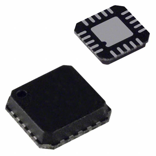
The bottom of the chip scale package has a central thermal pad.
The thermal pad on the printed circuit board should be at least
as large as this exposed pad. On the printed circuit board, there
should be a clearance of at least 0.25 mm between the thermal
pad and the inner edges of the pad pattern to ensure that shorting
is avoided.
The ADF4156 has a simple SPI-compatible serial interface for
writing to the device. CLOCK, DATA, and LE control the data
transfer. When latch enable (LE) is high, the 29 bits that have
been clocked into the input register on each rising edge of serial
clock are transferred to the appropriate latch. The maximum
allowable serial clock rate is 20 MHz. See Figure 2 for the timing
diagram and Table 6 for the latch truth table.
PCB DESIGN GUIDELINES FOR CHIP SCALE
PACKAGE
The lands on the lead frame chip scale package (CP-20-6) are
rectangular. The printed circuit board pad for these lands should be
0.1 mm longer than the package land length and 0.05 mm wider
than the package land width. The package land should be centered
on the pad to ensure that the solder joint size is maximized.
Thermal vias can be used on the printed circuit board thermal
pad to improve thermal performance of the package. If vias are
used, they should be incorporated in the thermal pad on a 1.2 mm
pitch grid. The via diameter should be between 0.3 mm and
0.33 mm, and the via barrel should be plated with 1 oz of
copper to plug the via. In addition, the printed circuit board
thermal pad should be connected to AGND.
Rev. E | Page 21 of 24
�ADF4156
Data Sheet
OUTLINE DIMENSIONS
5.10
5.00
4.90
16
9
4.50
4.40
4.30
6.40
BSC
1
8
PIN 1
1.20
MAX
0.15
0.05
0.20
0.09
0.30
0.19
0.65
BSC
COPLANARITY
0.10
0.75
0.60
0.45
8°
0°
SEATING
PLANE
COMPLIANT TO JEDEC STANDARDS MO-153-AB
Figure 25. 16-Lead Thin Shrink Small Outline Package [TSSOP]
(RU-16)
Dimensions shown in millimeters
0.30
0.25
0.18
0.50
BSC
PIN 1
INDICATOR
20
16
15
1
EXPOSED
PAD
2.30
2.10 SQ
2.00
11
TOP VIEW
0.80
0.75
0.70
0.65
0.60
0.55
5
10
0.20 MIN
BOTTOM VIEW
0.05 MAX
0.02 NOM
COPLANARITY
0.08
0.20 REF
SEATING
PLANE
6
FOR PROPER CONNECTION OF
THE EXPOSED PAD, REFER TO
THE PIN CONFIGURATION AND
FUNCTION DESCRIPTIONS
SECTION OF THIS DATA SHEET.
COMPLIANT TO JEDEC STANDARDS MO-220-WGGD-1.
08-16-2010-B
PIN 1
INDICATOR
4.10
4.00 SQ
3.90
Figure 26. 20-Lead Lead Frame Chip Scale Package [LFCSP_WQ]
4 mm × 4 mm Body, Very Very Thin Quad
(CP-20-6)
Dimensions shown in millimeters
ORDERING GUIDE
Model 1
ADF4156BRUZ
ADF4156BRUZ-RL
ADF4156BRUZ-RL7
ADF4156BCPZ
ADF4156BCPZ-RL
ADF4156BCPZ-RL7
EV-ADF4156SD1Z
1
Temperature Range
−40°C to +85°C
−40°C to +85°C
−40°C to +85°C
−40°C to +85°C
−40°C to +85°C
−40°C to +85°C
Package Description
16-Lead Thin Shrink Small Outline Package [TSSOP]
16-Lead Thin Shrink Small Outline Package [TSSOP]
16-Lead Thin Shrink Small Outline Package [TSSOP]
20-Lead Lead Frame Chip Scale Package [LFCSP_WQ]
20-Lead Lead Frame Chip Scale Package [LFCSP_WQ]
20-Lead Lead Frame Chip Scale Package [LFCSP_WQ]
Evaluation Board
Z = RoHS Compliant Part.
Rev. E | Page 22 of 24
Package Option
RU-16
RU-16
RU-16
CP-20-6
CP-20-6
CP-20-6
�Data Sheet
ADF4156
NOTES
Rev. E | Page 23 of 24
�ADF4156
Data Sheet
NOTES
I2C refers to a communications protocol originally developed by Philips Semiconductors (now NXP Semiconductors).
©2006–2013 Analog Devices, Inc. All rights reserved. Trademarks and
registered trademarks are the property of their respective owners.
D05863-0-10/13(E)
Rev. E | Page 24 of 24
�


 工商网监
湘ICP备2023018690号
工商网监
湘ICP备2023018690号
