FEATURES
FUNCTIONAL BLOCK DIAGRAM
Triaxis digital gyroscope with digital range scaling
±75°/sec, ±150°/sec, ±300°/sec settings
Tight orthogonal alignment: 5.25 V
(1 = power supply > 5.25 V, 0 = power supply ≤ 5.25 V)
Power supply < 4.75 V
(1 = power supply < 4.75 V, 0 = power supply ≥ 4.75 V)
Alarm Registers
The alarm function provides monitoring for two independent
conditions. The ALM_CTRL register provides control inputs
for data source, data filtering (prior to comparison), static
comparison, dynamic rate-of-change comparison, and output
indicator configurations. The ALM_MAGx registers establish
the trigger threshold and polarity configurations. Table 30 gives
an example of how to configure a static alarm. The ALM_SMPLx
registers provide the numbers of samples to use in the dynamic
rate-of-change configuration. The period equals the number in
the ALM_SMPLx register multiplied by the sample period time,
which is established by the SMPL_PRD register. See Table 31 for
an example of how to configure the sensor for this type of function.
Setting MSC_CTRL[11] = 1 (DIN = 0xB508) performs a
checksum verification of the flash memory locations. The
pass/fail result is loaded into DIAG_STAT[6].
Rev. F | Page 15 of 20
�ADIS16362
Data Sheet
Table 27. ALM_MAG1, ALM_MAG2 Bit Descriptions
Table 30. Alarm Configuration Example 1
Bit
[15]
DIN
0xAF55,
0xAE17
[14]
[13:0]
Description
Comparison polarity
(1 = greater than, 0 = less than)
Not used
Data bits that match the format of the trigger source
selection
Table 28. ALM_SMPL1, ALM_SMPL2 Bit Descriptions
Bit
[15:8]
[7:0]
Description
Not used
Data bits: number of samples (both 0x00 and 0x01 = 1)
Table 29. ALM_CTRL Bit Descriptions
Bit
[15:12]
[11:8]
[7]
[6]
[5]
[4]
[3]
[2]
[1]
[0]
Description
Alarm 2 source selection
0000 = disable
0001 = power supply output
0010 = x-axis gyroscope output
0011 = y-axis gyroscope output
0100 = z-axis gyroscope output
0101 = x-axis accelerometer output
0110 = y-axis accelerometer output
0111 = z-axis accelerometer output
1000 = x-axis gyroscope temperature output
1001 = y-axis gyroscope temperature output
1010 = z-axis gyroscope temperature output
1011 = auxiliary ADC input
Alarm 1 source selection (same as Alarm 2)
Rate-of-change (ROC) enable for Alarm 2
(1 = rate of change, 0 = static level)
Rate-of-change (ROC) enable for Alarm 1
(1 = rate of change, 0 = static level)
Not used
Comparison data filter setting
(1 = filtered data, 0 = unfiltered data)
Not used
Alarm output enable
(1 = enabled, 0 = disabled)
Alarm output polarity
(1 = active high, 0 = active low)
Alarm output line select
(1 = DIO2, 0 = DIO1)
0xA785,
0xA6DE
0xA93A,
0xA822
Description
ALM_CTRL = 0x5517
Alarm 1 input = XACCL_OUT
Alarm 2 input = XACCL_OUT
Static level comparison, filtered data
DIO2 output indicator, positive polarity
ALM_MAG1 = 0x85DE
Alarm 1 is true if XACCL_OUT > +0.5 g
ALM_MAG2 = 0x3A22
Alarm 2 is true if XACCL_OUT < −0.5 g
Table 31. Alarm Configuration Example 2
DIN
0xAF76,
0xAE87
0xB601
0xAA08
0xAC50
0xA785,
0xA6DE
0xA93A,
0xA822
Description
ALM_CTRL = 0x7687
Alarm 1 input = YACCL_OUT
Alarm 2 input = ZACCL_OUT
Rate-of-change comparison, unfiltered data
DIO2 output indicator, positive polarity
SMPL_PRD = 0x0001
Sample rate = 819.2 SPS
ALM_SMPL1 = 0x0008
Alarm 1 rate-of-change period = 9.77 ms
ALM_SMPL2 = 0x0050
Alarm 2 rate-of-change period = 97.7 ms
ALM_MAG1 = 0x85DE
Alarm 1 is true if XACCL_OUT > +0.5 g
ALM_MAG2 = 0x3A22
Alarm 2 is true if XACCL_OUT < −0.5 g
PRODUCT IDENTIFICATION
Table 32 provides a summary of the registers that identify
the product: PROD_ID, which identifies the product type;
LOT_ID1 and LOT_ID2, the 32-bit lot identification code;
and SERIAL_NUM, which displays the 12-bit serial number.
All four registers are two bytes in length. When using the
SERIAL_NUM value to calculate the serial number, mask
off the upper four bits and convert the remaining 12 bits to
a decimal number.
Table 32. Identification Registers
Register Name
LOT_ID1
LOT_ID2
PROD_ID
Address
0x52
0x54
0x56
SERIAL_NUM
0x58
Rev. F | Page 16 of 20
Description
Lot Identification Code 1
Lot Identification Code 2
Product identification = 0x3FEA
(hexadecimal number for 16,362)
Serial number, 0 to 4095
�Data Sheet
ADIS16362
APPLICATIONS INFORMATION
INSTALLATION/HANDLING
VCC
For ADIS16362 installation, use the following two-step process:
C1
For removal,
1.
2.
Gently pry the connector from its mate using a small slot
screwdriver.
Remove the screws and lift the part up.
Never attempt to unplug the connector by pulling on the plastic
case or baseplate. Although the flexible connector is very reliable
in normal operation, it can break when subjected to unreasonable
handling. When broken, the flexible connector cannot be repaired.
The AN-1041 Application Note provides more information
about developing an appropriate mechanical interface design.
Figure 16. Equivalent Analog Input Circuit
(Conversion Phase: Switch Open,
Track Phase: Switch Closed)
ADIS16IMU2/PCBZ
The ADIS16IMU2/PCBZ accessories provide a simplified
method for connecting the ADIS16362 to an embedded
processor platform or to the EVAL-ADIS2 evaluation system.
Figure 17 provides the pin assignments for J1 on the
ADIS16IMU2/PCBZ breakout board.
J1
GYROSCOPE BIAS OPTIMIZATION
The factory calibration addresses initial bias errors along with
temperature-dependent bias behaviors. Installation and certain
environmental conditions can introduce modest bias errors.
The precision autonull command (GLOB_CMD[4]) provides a
simple predeployment method for correcting these errors to an
accuracy of approximately 0.008°/sec, using an average of 30 sec.
Averaging the sensor output data for 100 sec can provide incremental performance gains, as well. Controlling device rotation,
power supply, and temperature during these averaging times
helps to ensure optimal accuracy during this process. Refer to
the AN-1041 Application Note for more information about
optimizing performance.
D
08179-014
Secure the baseplate using machine screws.
Press the connector into its mate.
R1 C2
RST
1
2
SCLK
CS
3
4
DOUT
DIN
DNC
5
6
GND
7
8
GND
GND
9
10
VDD
VDD
11
12
VDD
DIO1
13
14
DIO2
DIO3
15
16
DIO4/CLKIN
08179-211
1.
2.
D
Figure 17. J1 Pin Assignments for the ADIS16IMU2/PCBZ
The C1 and C2 locations on the ADIS16IMU2/PCBZ provide
users with the pads to install capacitance across VDD and
GND, which Figure 9 recommends for best performance.
PC-BASED EVALUATION TOOLS
INPUT ADC CHANNEL
The AUX_ADC register provides access to the auxiliary ADC
input channel. The ADC is a 12-bit successive approximation
converter that has an input circuit equivalent to the one shown
in Figure 16. The maximum input is 3.3 V. The ESD protection
diodes can handle 10 mA without causing irreversible damage.
The on resistance (R1) of the switch has a typical value of 100 Ω.
The sampling capacitor, C2, has a typical value of 16 pF.
The EVAL-ADIS2 supports PC-based evaluation of the
ADIS16362. Refer to the EVAL-ADIS2 Evaluation System Wiki
Guide for more information on connecting the ADIS16362 to
the EVAL-ADIS2 system.
X-RAY SENSITIVITY
Exposure to high dose rate X-rays, such as those in production
systems that inspect solder joints in electronic assemblies, may
affect accelerometer bias errors. For optimal performance, avoid
exposing the ADIS16362 to this type of inspection.
Rev. F | Page 17 of 20
�ADIS16362
Data Sheet
OUTLINE DIMENSIONS
31.900
31.700
31.500
23.454
23.200
22.946
TOP VIEW
2.382
BSC
22.964
22.710
22.456
10.60
BSC
10.50
BSC
BOTTOM VIEW
6.732
6.605
6.478
5.20
5.00
4.80
(2×)
14.950
14.550
14.150
PIN 24
4.20
4.00
3.80
(2×)
17.41
17.21
17.01
(2×)
1.588
BSC
1.588
BSC
26.827
26.700
26.573
9.464
9.210
8.956
(2×)
21.410
21.210
21.010
14.732
14.605
14.478
CASTING
FEATURE
7.18
BSC
1.00
BSC
PIN 1
0.05
BSC
5.18
BSC
12.10
BSC
2.00 BSC
FRONT VIEW
23.504
23.250
22.996
2.660
2.500
2.340
SIDE VIEW
4.33
BSC
DETAIL A
DETAIL A
1.00
BSC (22×)
1.65 BSC
14.00 BSC
04-21-2017-E
0.305
BSC (24×)
4.162 BSC
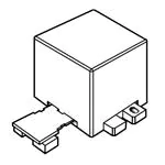
Figure 18. 24-Lead Module with Connector Interface
(ML-24-2)
Dimensions shown in millimeters
ORDERING GUIDE
Model 1
ADIS16362BMLZ
ADIS16IMU2/PCBZ
EVAL-ADIS2
1
Temperature Range
−40°C to +105°C
Package Description
24-Lead Module with Connector Interface
Breakout board
Evaluation System
Z = RoHS Compliant Part.
Rev. F | Page 18 of 20
Package Option
ML-24-2
�Data Sheet
ADIS16362
NOTES
Rev. F | Page 19 of 20
�ADIS16362
Data Sheet
NOTES
©2009–2019 Analog Devices, Inc. All rights reserved. Trademarks and
registered trademarks are the property of their respective owners.
D08179-0-3/19(F)
Rev. F | Page 20 of 20
�