GND
3
ATTIN
4
D2
GND
LE
14
13
PARALLEL
INTERFACE
4-BIT DIGITAL
ATTENUATOR
5
6
7
12
VDD
11
VSS
10
GND
9
ATTOUT
8
PACKAGE
BASE
GND
20424-001
2
15
GND
1
D5
16
GND
D4
D3
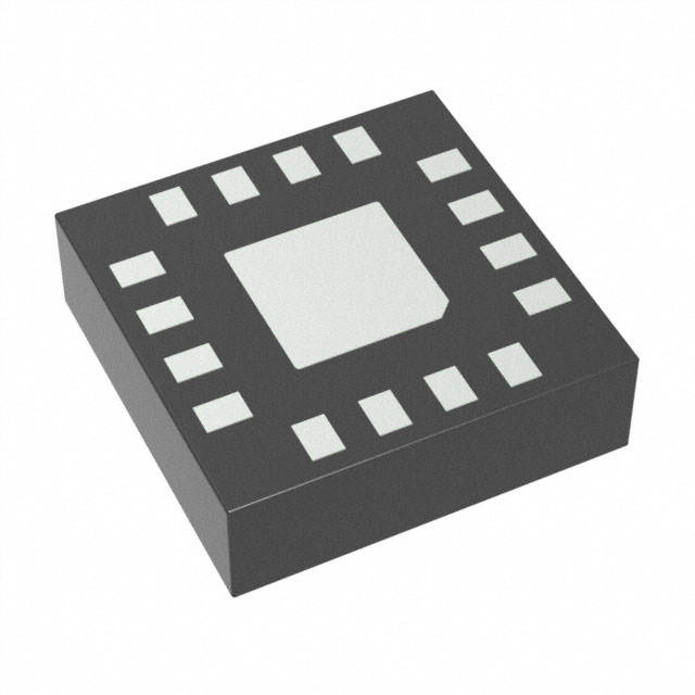
FUNCTIONAL BLOCK DIAGRAM
Ultrawideband frequency range: 10 MHz to 60 GHz
Attenuation range: 2 dB steps to 22 dB
Low insertion loss
1.4 dB up to 20 GHz
2.2 dB up to 44 GHz
3.3 dB up to 55 GHz
Attenuation accuracy
±(0.1 + 1.0% of state) up to 20 GHz
±(0.2 + 3.0% of state) up to 44 GHz
±(0.2 + 7.0% of state) up to 55 GHz
Typical step error
±0.30 dB up to 20 GHz
±0.50 dB up to 44 GHz
±0.60 dB up to 55 GHz
High input linearity
P0.1dB: 25.5 dBm typical
IP3: 45 dBm typical
High RF input power handling: 24 dBm average, 24 dBm peak
Tight distribution in relative phase
No low frequency spurious signals
Parallel mode control, CMOS and LVTTL compatible
RF amplitude settling time (0.1 dB of final RF output): 175 ns
16-terminal, 2.5 mm × 2.5 mm, RoHS compliant LGA package
GND
FEATURES
GND
Data Sheet
2 dB LSB, 4-Bit, Silicon Digital Attenuator,
10 MHz to 60 GHz
ADRF5740
Figure 1.
APPLICATIONS
Industrial scanners
Test and instrumentation
Cellular infrastructure: 5G millimeter wave
Military radios, radars, electronic counter measures (ECMs)
Microwave radios and very small aperture terminals (VSATs)
GENERAL DESCRIPTION
The ADRF5740 is a silicon, 4-bit digital attenuator with 22 dB
attenuation control range in 2 dB steps.
The ADRF5740 operates from 10 MHz to 60 GHz with less than
3.3 dB of insertion loss and with ±(0.2 + 7.0% of attenuation state)
of attenuation accuracy at 55 GHz. The ATTIN port of the
ADRF5740 has an RF input power handling capability of 24 dBm
average and 24 dBm peak for all states.
Rev. 0
The ADRF5740 requires a dual supply voltage of +3.3 V and
−3.3 V. The ADRF5740 features parallel mode control, and
CMOS- and low voltage transistor to transistor logic (LVTTL)compatible controls.
The ADRF5740 RF ports are designed to match a characteristic
impedance of 50 Ω. The ADRF5740 comes in a 16-terminal,
2.5 mm × 2.5 mm, RoHS compliant, land grid array (LGA)
package and operates from −40°C to +105°C.
Document Feedback
Information furnished by Analog Devices is believed to be accurate and reliable. However, no
responsibility is assumed by Analog Devices for its use, nor for any infringements of patents or other
rights of third parties that may result from its use. Specifications subject to change without notice.
No license is granted by implication or otherwise under any patent or patent rights of Analog
Devices. Trademarks and registered trademarks are the property of their respective owners.
One Technology Way, P.O. Box 9106, Norwood, MA 02062-9106, U.S.A.
Tel: 781.329.4700
©2020 Analog Devices, Inc. All rights reserved.
Technical Support
www.analog.com
�ADRF5740
Data Sheet
TABLE OF CONTENTS
Features .............................................................................................. 1
Applications ...................................................................................... 1
Insertion Loss, Return Loss, State Error, Step Error, and
Relative Phase ................................................................................7
Functional Block Diagram .............................................................. 1
Input Power Compression and Third-Order Intercept ..........9
General Description ......................................................................... 1
Theory of Operation ...................................................................... 10
Revision History ............................................................................... 2
Power Supply .............................................................................. 10
Specifications .................................................................................... 3
RF Input and Output ................................................................. 10
Electrical Specifications ............................................................... 3
Parallel Mode Interface ............................................................. 11
Timing Specifications .................................................................. 4
Applications Information ............................................................. 12
Absolute Maximum Ratings ....................................................... 5
Layout Considerations .............................................................. 12
Electrostatic Discharge (ESD) Ratings ...................................... 5
Board Layout............................................................................... 12
Thermal Resistance ...................................................................... 5
RF and Digital Controls ............................................................ 12
Power Derating Curves ............................................................... 5
Packaging and Ordering Information ......................................... 13
ESD Caution.................................................................................. 5
Outline Dimensions ................................................................... 13
Pin Configuration and Function Descriptions ............................ 6
Ordering Guide .......................................................................... 13
Interface Schematics .................................................................... 6
Typical Performance Characteristics ............................................. 7
REVISION HISTORY
6/2020—Revision 0: Initial Version
Rev. 0 | Page 2 of 13
�Data Sheet
ADRF5740
SPECIFICATIONS
ELECTRICAL SPECIFICATIONS
VDD = 3.3 V, VSS = −3.3 V, digital voltages = 0 V or VDD, TCASE = 25°C, and a 50 Ω system, unless otherwise noted.
Table 1.
Parameter
FREQUENCY RANGE
INSERTION LOSS
RETURN LOSS
ATTENUATION
Range
Step Size
Accuracy
Step Error
RELATIVE PHASE
SWITCHING CHARACTERISTICS
Rise and Fall Time (tRISE and tFALL)
On and Off Time (tON and tOFF)
RF Amplitude Settling Time
0.1 dB
0.05 dB
Overshoot
Undershoot
RF Phase Settling Time
5°
1°
Test Conditions/Comments
10 MHz to 20 GHz
20 GHz to 44 GHz
44 GHz to 55 GHz
55 GHz to 60 GHz
ATTIN and ATTOUT, all attenuation states
10 MHz to 20 GHz
20 GHz to 44 GHz
44 GHz to 55 GHz
55 GHz to 60 GHz
1.4
2.2
3.3
4.4
Unit
MHz
dB
dB
dB
dB
14
13
12
10
dB
dB
dB
dB
Between minimum and maximum
attenuation states
Between any successive attenuation states
Referenced to insertion loss
10 MHz to 20 GHz
20 GHz to 44 GHz
44 GHz to 55 GHz
55 GHz to 60 GHz
Between any successive state
10 MHz to 20 GHz
20 GHz to 44 GHz
44 GHz to 55 GHz
55 GHz to 60 GHz
Referenced to insertion loss
10 MHz to 20 GHz
20 GHz to 44 GHz
44 GHz to 55 GHz
55 GHz to 60 GHz
All attenuation states at input power =
10 dBm
10% to 90% of RF output
50% triggered control to 90% of RF output
22
dB
2
dB
±(0.1 + 1.0% of state)
±(0.2 + 3.0% of state)
±(0.2 + 7.0% of state)
±(0.3 + 7.0% of state)
dB
dB
dB
dB
±0.30
±0.50
±0.60
±1.2
dB
dB
dB
dB
22
55
65
70
Degrees
Degrees
Degrees
Degrees
50
100
ns
ns
175
ns
225
ns
2
0.75
dB
dB
105
120
ns
ns
50% triggered control to 0.1 dB of final RF
output
50% triggered control to 0.05 dB of final
RF output
f = 40 GHz
50% triggered control to 5° of final RF output
50% triggered control to 1° of final RF output
Rev. 0 | Page 3 of 13
Min
10
Typ
Max
60,000
�ADRF5740
Data Sheet
Parameter
INPUT LINEARITY1
0.1 dB Power Compression (P0.1dB)
1 dB Power Compression (P1dB)
Third-Order Intercept (IP3)
DIGITAL CONTROL INPUTS
Voltage
Low (VINL)
High (VINH)
Current
Low (IINL)
High (IINH)
SUPPLY CURRENT
Positive Supply Current (IDD)
Bias Low
Bias High
Negative Supply Current (ISS)
RECOMMENDED OPERATING CONDITIONS
Supply Voltage
VDD
VSS
Digital Control Voltage
RF Power2
Input at ATTIN
Input at ATTOUT
Test Conditions/Comments
100 MHz to 50 GHz
Min
Typ
Max
25.5
26.5
45
Two-tone input power = 12 dBm per tone,
Δf = 1 MHz, all attenuation states
LE, D2, D3, D4, D5 pins
Unit
dBm
dBm
dBm
0
1.2
0.8
3.3
V
V
LE, D2, D3, D4, D5 pins
−10
很抱歉,暂时无法提供与“ADRF5740BCCZN”相匹配的价格&库存,您可以联系我们找货
免费人工找货