400 MHz to 1250 MHz Quadrature Modulator with
750 MHz to 1150 MHz Frac-N PLL and Integrated VCO
ADRF6701
Data Sheet
FEATURES
modulator, PLL, and VCO provides for significant board
savings and reduces the BOM and design complexity.
IQ modulator with integrated fractional-N PLL
Output frequency range: 400 MHz to 1250 MHz
Internal LO frequency range: 750 MHz to 1150 MHz
Output P1dB: 10.3 dBm @ 1100 MHz
Output IP3: 30.1 dBm @ 1100 MHz
Noise floor: −159.4 dBm/Hz @ 1100 MHz
Baseband bandwidth: 750 MHz (3 dB)
SPI serial interface for PLL programming
Integrated LDOs and LO buffer
Power supply: 5 V/240 mA
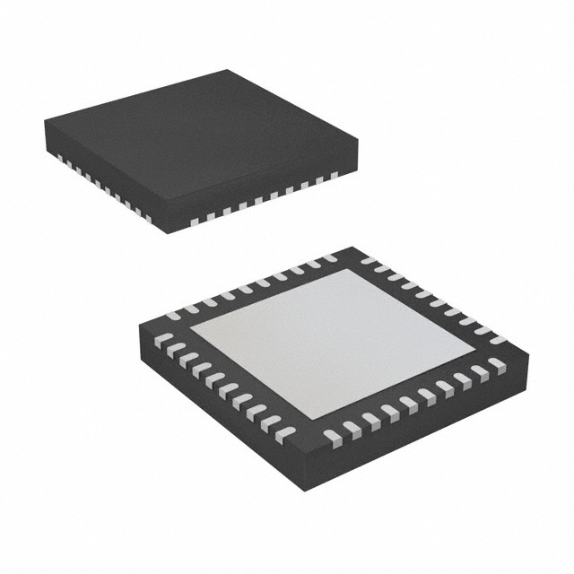
40-lead 6 mm × 6 mm LFCSP
The integrated fractional-N PLL/synthesizer generates a 2× fLO
input to the IQ modulator. The phase detector together with an
external loop filter is used to control the VCO output. The VCO
output is applied to a quadrature divider. To reduce spurious
components, a sigma-delta (Σ-Δ) modulator controls the
programmable PLL divider.
The IQ modulator has wideband differential I and Q inputs,
which support baseband as well as complex IF architectures.
The single-ended modulator output is designed to drive a 50 Ω
load impedance and can be disabled.
APPLICATIONS
The ADRF6701 is fabricated using an advanced silicon-germanium
BiCMOS process. It is available in a 40-lead, exposed-paddle, Pbfree, 6 mm × 6 mm LFCSP package. Performance is specified from
−40°C to +85°C. A lead-free evaluation board is available.
Cellular communications systems
GSM/EDGE, CDMA2000, W-CDMA, TD-SCDMA, LTE
Broadband wireless access systems
Satellite modems
Table 1.
GENERAL DESCRIPTION
Part No.
ADRF6701
The ADRF6701 provides a quadrature modulator and
synthesizer solution within a small 6 mm × 6 mm footprint
while requiring minimal external components.
ADRF6702
The ADRF6701 is designed for RF outputs from 400 MHz to
1250 MHz. The low phase noise VCO and high performance
quadrature modulator make the ADRF6701 suitable for next
generation communication systems requiring high signal
dynamic range and linearity. The integration of the IQ
IQ Modulator
±3 dB RF Output Range
400 MHz
1250 MHz
1200 MHz
2400 MHz
1550 MHz
2650 MHz
2050
3000 MHz
Internal LO Range
750 MHz
1150 MHz
1550 MHz
2150 MHz
2100 MHz
2600 MHz
2500 MHz
290 MHz
ADRF6703
ADRF6704
FUNCTIONAL BLOCK DIAGRAM
VCC7
VCC6
VCC5
VCC4
VCC3
VCC2
VCC1
34
29
27
22
17
10
1
LOSEL 36
ADRF6701
LON 37
BUFFER
LOP 38
BUFFER
CLK 13
SPI
INTERFACE
LE 14
MODULUS
THIRD-ORDER
FRACTIONAL
INTERPOLATOR
×2
REFIN 6
÷2
N COUNTER
21 TO 123
TEMP
SENSOR
÷4
MUXOUT 8
4
7
11 15 20 21 23 25 28 30 31 35
GND
÷2
0/90
CHARGE PUMP
250µA,
500µA (DEFAULT),
750µA,
1000µA
–
PHASE
+ FREQUENCY
DETECTOR
5
RSET
NOTES
1. NC = NO CONNECT. DO NOT CONNECT TO THIS PIN.
DECL1
19 QN
32 IN
33 IP
3
24
NC
DECL2
2
18 QP
VCO
CORE
PRESCALER
÷2
MUX
DIVIDER
÷2
2:1
MUX
INTEGER
REG
9
39
16
26
CP VTUNE ENOP RFOUT
08567-001
FRACTION
REG
DATA 12
40 DECL3
DIVIDER
÷2
Figure 1.
Rev. A
Information furnished by Analog Devices is believed to be accurate and reliable. However, no
responsibility is assumed by Analog Devices for its use, nor for any infringements of patents or other
rights of third parties that may result from its use. Specifications subject to change without notice. No
license is granted by implication or otherwise under any patent or patent rights of Analog Devices.
Trademarks and registered trademarks are the property of their respective owners.
One Technology Way, P.O. Box 9106, Norwood, MA 02062-9106, U.S.A.
Tel: 781.329.4700
www.analog.com
Fax: 781.461.3113 ©2011–2012 Analog Devices, Inc. All rights reserved.
�ADRF6701
Data Sheet
TABLE OF CONTENTS
Features .............................................................................................. 1
Device Programming and Register Sequencing..................... 19
Applications ....................................................................................... 1
Register Summary .......................................................................... 20
General Description ......................................................................... 1
Register Description....................................................................... 21
Functional Block Diagram .............................................................. 1
Register 0—Integer Divide Control (Default: 0x0001C0) .... 21
Revision History ............................................................................... 2
Register 1—Modulus Divide Control (Default: 0x003001) .. 22
Specifications..................................................................................... 3
Register 2—Fractional Divide Control (Default: 0x001802) 22
Timing Characteristics ................................................................ 6
Register 3—Σ-Δ Modulator Dither Control (Default:
0x10000B) .................................................................................... 23
Absolute Maximum Ratings............................................................ 7
ESD Caution .................................................................................. 7
Pin Configuration and Function Descriptions ............................. 8
Typical Performance Characteristics ........................................... 10
Theory of Operation ...................................................................... 16
Register 4—PLL Charge Pump, PFD, and Reference Path
Control (Default: 0x0AA7E4)................................................... 24
Register 5—LO Path and Modulator Control (Default:
0x0000D5) ................................................................................... 26
PLL + VCO .................................................................................. 16
Register 6—VCO Control and VCO Enable (Default:
0x1E2106) .................................................................................... 27
Basic Connections for Operation ............................................. 16
Register 7—External VCO Enable and Second lo divider .... 27
External LO ................................................................................. 16
Characterization Setups ................................................................. 28
Loop Filter ................................................................................... 17
Evaluation Board ............................................................................ 30
DAC-to-IQ Modulator Interfacing .......................................... 18
Evaluation Board Control Software ......................................... 30
Adding a Swing-Limiting Resistor ........................................... 18
Outline Dimensions ....................................................................... 35
IQ Filtering .................................................................................. 19
Ordering Guide .......................................................................... 35
Baseband Bandwidth ................................................................. 19
REVISION HISTORY
6/12—Rev. 0 to Rev. A
Changes to Table 1 ............................................................................ 1
Changes to the Device Programming and Register
Sequencing Section ........................................................................ 19
Changes to Figure 45 ...................................................................... 25
9/11—Revision 0: Initial Version
Rev. A | Page 2 of 36
�Data Sheet
ADRF6701
SPECIFICATIONS
VS = 5 V; TA = 25°C; baseband I/Q amplitude = 1 V p-p differential sine waves in quadrature with a 500 mV dc bias; baseband I/Q
frequency (fBB) = 1 MHz; fPFD = 38.4 MHz; fREF = 153.6 MHz at +4 dBm Re:50 Ω (1 V p-p); 130 kHz loop filter, unless otherwise noted.
Table 2.
Parameter
Test Conditions/Comments
Min
OPERATING FREQUENCY RANGE
IQ modulator (±3 dB RF output range)
PLL LO range
RFOUT pin
Baseband VIQ = 1 V p-p differential
RF output divided by baseband input voltage
400
750
RF OUTPUT = 800 MHz
Nominal Output Power
IQ Modulator Voltage Gain
OP1dB
Carrier Feedthrough
Sideband Suppression
Quadrature Error
I/Q Amplitude Balance
Second Harmonic
Third Harmonic
Output IP2
Output IP3
Noise Floor
POUT − P (fLO ± (2 × fBB))
POUT − P (fLO ± (3 × fBB))
f1BB = 3.5 MHz, f2BB = 4.5 MHz, POUT ≈ −2 dBm per tone
f1BB = 3.5 MHz, f2BB = 4.5 MHz, POUT ≈ −2 dBm per tone
I/Q inputs = 0 V differential with 500 mV dc bias, 20 MHz carrier offset
RF OUTPUT = 950 MHz
Nominal Output Power
IQ Modulator Voltage Gain
OP1dB
Carrier Feedthrough
Sideband Suppression
Quadrature Error
I/Q Amplitude Balance
Second Harmonic
Third Harmonic
Output IP2
Output IP3
Noise Floor
RFOUT pin
Baseband VIQ = 1 V p-p differential
RF output divided by baseband input voltage
RF OUTPUT = 1100 MHz
Nominal Output Power
IQ Modulator Voltage Gain
OP1dB
Carrier Feedthrough
Sideband Suppression
Quadrature Error
I/Q Amplitude Balance
Second Harmonic
Third Harmonic
Output IP2
Output IP3
Noise Floor
SYNTHESIZER SPECIFICATIONS
Internal LO Range
Figure of Merit (FOM) 1
RFOUT pin
Baseband VIQ = 1 V p-p differential
RF output divided by baseband input voltage
POUT − P (fLO ± (2 × fBB))
POUT − P (fLO ± (3 × fBB))
f1BB = 3.5 MHz, f2BB = 4.5 MHz, POUT ≈ −2 dBm per tone
f1BB = 3.5 MHz, f2BB = 4.5 MHz, POUT ≈ −2 dBm per tone
I/Q inputs = 0 V differential with 500 mV dc bias, 20 MHz carrier offset
POUT − P (fLO ± (2 × fBB))
POUT − P (fLO ± (3 × fBB))
f1BB = 3.5 MHz, f2BB = 4.5 MHz, POUT ≈ −2 dBm per tone
f1BB = 3.5 MHz, f2BB = 4.5 MHz, POUT ≈ −2 dBm per tone)
I/Q inputs = 0 V differential with 500 mV dc bias, 20 MHz carrier offset
Synthesizer specifications referenced to the modulator output
Typ
Unit
1250
1150
MHz
MHz
4.4
0.4
12.5
−49.9
−53.9
−0.75
0.03
−81.9
−58.8
>70
30.8
−157.9
dBm
dB
dBm
dBm
dBc
Degrees
dB
dBc
dBc
dBm
dBm
dBm/Hz
3.8
−0.2
11.2
−46.2
−45.4
−0.5
0.03
−76.5
−59.1
>70
31.7
−157.9
dBm
dB
dBm
dBm
dBc
Degrees
dB
dBc
dBc
dBm
dBm
dBm/Hz
2.1
−1.9
10.3
−49.9
−47.2
−0.5
0.03
−77.7
−60.3
>70
30.1
−159.4
dBm
dB
dBm
dBm
dBc
Degrees
dB
dBc
dBc
dBm
dBm
dBm/Hz
750
1150
−222
Rev. A | Page 3 of 36
Max
MHz
dBc/Hz/Hz
�ADRF6701
Data Sheet
Parameter
Test Conditions/Comments
REFERENCE CHARACTERISTICS
REFIN Input Frequency
REFIN Input Capacitance
Phase Detector Frequency
MUXOUT Output Level
REFIN, MUXOUT pins
Min
12
20
Integrated Phase Noise
Reference Spurs
PHASE NOISE (FREQUENCY =
Unit
160
MHz
pF
MHz
V
40
0.25
Low (lock detect output selected)
High (lock detect output selected)
PHASE NOISE (FREQUENCY =
800 MHz, fPFD = 38.4 MHz)
Max
4
2.7
MUXOUT Duty Cycle
CHARGE PUMP
Charge Pump Current
Output Compliance Range
Typ
V
50
Programmable to 250 µA, 500 µA, 750 µA, 1000 µA
%
500
1
2.8
µA
V
Closed loop operation (see Figure 35 for loop filter design)
10 kHz offset
100 kHz offset
1 MHz offset
10 MHz offset
1 kHz to 10 MHz integration bandwidth
fPFD/2
fPFD
fPFD × 2
fPFD × 3
fPFD × 4
Closed loop operation (see Figure 35 for loop filter design)
−114
−112
−135
−154
0.09
−113
−101
−99
−108
−99
dBc/Hz
dBc/Hz
dBc/Hz
dBc/Hz
10 kHz offset
100 kHz offset
1 MHz offset
10 MHz offset
1 kHz to 10 MHz integration bandwidth
fPFD/2
fPFD
fPFD × 2
fPFD × 3
fPFD × 4
Closed loop operation (see Figure 35 for loop filter design)
−112
−111
−133
−153
0.11
−113
−106
−104
−100
−107
dBc/Hz
dBc/Hz
dBc/Hz
dBc/Hz
°rms
dBc
dBc
dBc
dBc
dBc
10 kHz offset
100 kHz offset
1 MHz offset
10 MHz offset
1 kHz to 10 MHz integration bandwidth
fPFD/2
fPFD
fPFD × 2
fPFD × 3
fPFD × 4
Measured at RFOUT, frequency = 1100 MHz
Second harmonic
Third harmonic
−113
−108
−135
−153
0.12
−112
−93
−93
−105
−103
dBc/Hz
dBc/Hz
dBc/Hz
dBc/Hz
°rms
dBc
dBc
dBc
dBc
dBc
−61
−73
dBc
dBc
°rms
dBc
dBc
dBc
dBc
dBc
950 MHz, fPFD = 38.4 MHz)
Integrated Phase Noise
Reference Spurs
PHASE NOISE (FREQUENCY =
1100 MHz, fPFD = 38.4 MHz)
Integrated Phase Noise
Reference Spurs
RF OUTPUT HARMONICS
Rev. A | Page 4 of 36
�Data Sheet
ADRF6701
Parameter
Test Conditions/Comments
LO INPUT/OUTPUT
Output Frequency Range
LOP, LON
Divide by 4 circuit in LO path enabled
Divide by 2 circuit in LO path disabled
Dividers in LO path disabled
2× LO or 1× LO mode, into a 50 Ω load, LO buffer enabled
Externally applied 2× LO, PLL disabled
Externally applied 2× LO, PLL disabled
IP, IN, QP, QN pins
LO Output Level at 950 MHz
LO Input Level
LO Input Impedance
BASEBAND INPUTS
I and Q Input DC Bias Level
Bandwidth
Differential Input Impedance
Differential Input Capacitance
LOGIC INPUTS
Input High Voltage, VINH
Input Low Voltage, VINL
Input Current, IINH/IINL
Input Capacitance, CIN
TEMPERATURE SENSOR
Output Voltage
Temperature Coefficient
POWER SUPPLIES
Voltage Range
Supply Current
1
Min
Typ
750
1500
3000
Max
Unit
1150
2300
4600
MHz
MHz
MHz
dBm
dBm
Ω
600
mV
2.5
0
50
400
POUT ≈ −7 dBm, RF flatness of IQ modulator output calibrated out
0.5 dB
3 dB
500
350
750
920
1
MHz
MHz
Ω
pF
CLK, DATA, LE, ENOP, LOSEL
1.4
0
3.3
0.7
0.1
5
VPTAT voltage measured at MUXOUT
TA = 25°C, RL ≥10 kΩ (LO buffer disabled)
TA = −40°C to +85°C, RL ≥10 kΩ
VCC1, VCC2, VCC3, VCC4, VCC5, VCC6, VCC7
1.63
3.75
4.75
Normal Tx mode (PLL and IQMOD enabled, LO buffer disabled)
Tx mode using external LO input (internal VCO/PLL disabled)
Tx mode with LO buffer enabled
Power-down mode
5
240
130
290
22
V
V
µA
pF
V
mV/°C
5.25
V
mA
mA
mA
µA
The figure of merit (FOM) is computed as phase noise (dBc/Hz) – 10log10(fPFD) – 20log10(fLO/fPFD). The FOM was measured across the full LO range, with fREF = 80 MHz,
fREF power = 10 dBm (500 V/μs slew rate) with a 40 MHz fPFD. The FOM was computed at 50 kHz offset.
Rev. A | Page 5 of 36
�ADRF6701
Data Sheet
TIMING CHARACTERISTICS
Table 3.
Parameter
t1
t2
t3
t4
t5
t6
t7
Limit
20
10
10
25
25
10
20
Unit
ns min
ns min
ns min
ns min
ns min
ns min
ns min
Test Conditions/Comments
LE to CLK setup time
DATA to CLK setup time
DATA to CLK hold time
CLK high duration
CLK low duration
CLK to LE setup time
LE pulse width
t4
t5
CLK
t3
t2
DATA
DB23 (MSB)
DB22
DB2
(CONTROL BIT C3)
DB1
(CONTROL BIT C2)
DB0 (LSB)
(CONTROL BIT C1)
t7
t1
08567-002
t6
LE
Figure 2. Timing Diagram
Rev. A | Page 6 of 36
�Data Sheet
ADRF6701
ABSOLUTE MAXIMUM RATINGS
Table 4.
Parameter
Supply Voltage (VCC1 to VCC7)
Digital I/O, CLK, DATA, LE
LOP, LON
IP, IN, QP, QN
REFIN
θJA (Exposed Paddle Soldered Down)1
Maximum Junction Temperature
Operating Temperature Range
Storage Temperature Range
1
Rating
5.5 V
−0.3 V to +3.6 V
18 dBm
−0.5 V to +1.5 V
−0.3 V to +3.6 V
35°C/W
150°C
−40°C to +85°C
−65°C to +150°C
Stresses above those listed under Absolute Maximum Ratings
may cause permanent damage to the device. This is a stress
rating only; functional operation of the device at these or any
other conditions above those indicated in the operational
section of this specification is not implied. Exposure to absolute
maximum rating conditions for extended periods may affect
device reliability.
ESD CAUTION
Per JDEC standard JESD 51-2.
Rev. A | Page 7 of 36
�ADRF6701
Data Sheet
40
39
38
37
36
35
34
33
32
31
DECL3
VTUNE
LOP
LON
LOSEL
GND
VCC7
IP
IN
GND
PIN CONFIGURATION AND FUNCTION DESCRIPTIONS
PIN 1
INDICATOR
ADRF6701
TOP VIEW
(Not to Scale)
30
29
28
27
26
25
24
23
22
21
GND
VCC6
GND
VCC5
RFOUT
GND
NC
GND
VCC4
GND
NOTES
1. NC = NO CONNECT. DO NOT CONNECT TO THIS PIN.
2. THE EXPOSED PADDLE SHOULD BE SOLDERED TO A
LOW IMPEDANCE GROUND PLANE.
08567-003
GND
DATA
CLK
LE
GND
ENOP
VCC3
QP
QN
GND
11
12
13
14
15
16
17
18
19
20
VCC1 1
DECL1 2
CP 3
GND 4
RSET 5
REFIN 6
GND 7
MUXOUT 8
DECL2 9
VCC2 10
Figure 3. Pin Configuration
Table 5. Pin Function Descriptions
Pin No.
1, 10, 17, 22, 27, 29, 34
2
Mnemonic
VCC1, VCC2, VCC3,
VCC4, VCC5, VCC6,
VCC7
DECL1
3
CP
4, 7, 11, 15, 20, 21, 23,
25, 28, 30, 31, 35
24
5
GND
NC
RSET
Description
Power Supply Pins. The power supply voltage range is 4.75 V to 5.25 V. Drive all of
these pins from the same power supply voltage. Decouple each pin with 100 pF and
0.1 µF capacitors located close to the pin.
Decoupling Node for Internal 3.3 V LDO. Decouple this pin with 100 pF and 0.1 µF
capacitors located close to the pin.
Charge Pump Output Pin. Connect VTUNE to this pin through the loop filter. If
an external VCO is being used, connect the output of the loop filter to the VCO’s
voltage control pin. The PLL control loop should then be closed by routing the VCO’s
frequency output back into the ADRF6701 through the LON and LOP pins.
Ground. Connect these pins to a low impedance ground plane.
Do not connect to this pin.
Charge Pump Current. The nominal charge pump current can be set to 250 µA, 500 µA,
750 µA, or 1000 µA using DB10 and DB11 of Register 4 and by setting DB18 to 0 (CP
reference source).
In this mode, no external RSET is required. If DB18 is set to 1, the four nominal charge
pump currents (INOMINAL) can be externally tweaked according to the following
equation:
217.4 × I CP
R SET =
I NOMINAL
6
REFIN
8
MUXOUT
9
DECL2
12
DATA
− 37.8 Ω
where ICP is the base charge pump current in microamps. For further details on the
charge pump current, see the Register 4—PLL Charge Pump, PFD, and Reference Path
Control section.
Reference Input. The nominal input level is 1 V p-p. Input range is 12 MHz to 160 MHz.
This pin has high input impedance and should be ac-coupled. If REFIN is being driven
by laboratory test equipment, the pin should be externally terminated with a 50 Ω
resistor (place the ac-coupling capacitor between the pin and the resistor). When
driven from an 50 Ω RF signal generator, the recommended input level is 4 dBm.
Multiplexer Output. This output allows a digital lock detect signal, a voltage
proportional to absolute temperature (VPTAT), or a buffered, frequency-scaled
reference signal to be accessed externally. The output is selected by programming
DB21 to DB23 in Register 4.
Decoupling Node for 2.5 V LDO. Connect 100 pF, 0.1 µF, and 10 µF capacitors between this
pin and ground.
Serial Data Input. The serial data input is loaded MSB first with the three LSBs being
the control bits.
Rev. A | Page 8 of 36
�Data Sheet
ADRF6701
Pin No.
13
Mnemonic
CLK
14
LE
16
18, 19, 32, 33
ENOP
QP, QN, IN, IP
26
RFOUT
36
LOSEL
37, 38
LON, LOP
39
VTUNE
40
DECL3
EP
Description
Serial Clock Input. This serial clock input is used to clock in the serial data to the
registers. The data is latched into the 24-bit shift register on the CLK rising edge.
Maximum clock frequency is 20 MHz.
Latch Enable. When the LE input pin goes high, the data stored in the shift registers is
loaded into one of the six registers, the relevant latch being selected by the first three
control bits of the 24-bit word.
Modulator Output Enable/Disable. See Table 6.
Modulator Baseband Inputs. Differential in-phase and quadrature baseband inputs.
These inputs should be dc-biased to 0.5 V.
RF Output. Single-ended, 50 Ω internally biased RF output. RFOUT must be ac-coupled
to its load.
LO Select. This digital input pin determines whether the LOP and LON pins operate as
inputs or outputs. This pin should not be left floating. LOP and LON become inputs if
the LOSEL pin is set low and the LDRV bit of Register 5 is set low. In addition to setting
LOSEL and LDRV low and providing an external 2× LO, the LXL bit of Register 5 (DB4)
must be set to 1 to direct the external LO to the IQ modulator. LON and LOP become
outputs when LOSEL is high or if the LDRV bit of Register 5 (DB3) is set to 1. A 1× LO or
2× LO output can be selected by setting the LDIV bit of Register 5 (DB5) to 1 or 0
respectively (see Table 7).
Local Oscillator Input/Output. The internally generated 1× LO or 2× LO is available on
these pins. When internal LO generation is disabled, an external 1× LO or 2× LO can be
applied to these pins.
VCO Control Voltage Input. This pin is driven by the output of the loop filter. Nominal
input voltage range on this pin is 1.3 V to 2.5 V. If the external VCO mode is activated,
this pin can be left open.
Decoupling Node for VCO LDO. Connect a 100 pF capacitor and a 10 µF capacitor
between this pin and ground.
Exposed Paddle. The exposed paddle should be soldered to a low impedance
ground plane.
Table 6. Enabling RFOUT
ENOP
X1
0
1
1
Register 5 Bit DB6
0
X1
1
RFOUT
Disabled
Disabled
Enabled
X = don’t care.
Table 7. LO Port Configuration 1, 2
LON/LOP
Function
LOSEL
Register 5 Bit
DB5 (LDIV)
Register 5 Bit
DB4 (LXL)
Register 5 Bit
DB3 (LDRV)
Register 7 Bit
DB4 (LDIV2)
Input (4× LO)
Input (2× LO)
Output (Disabled)
Output (1× LO)
Output (1× LO)
Output (1× LO)
Output (2× LO)
Output (2× LO)
Output (2× LO)
0
0
0
0
1
1
0
1
1
X
X
X
0
0
0
1
1
1
1
1
0
0
0
0
0
0
0
0
0
0
1
0
1
1
0
1
0
1
X
0
0
0
0
0
0
1
2
X = don’t care.
LOSEL should not be left floating.
Rev. A | Page 9 of 36
�ADRF6701
Data Sheet
TYPICAL PERFORMANCE CHARACTERISTICS
VS = 5 V; TA = 25°C; baseband I/Q amplitude = 1 V p-p differential sine waves in quadrature with a 500 mV dc bias; baseband I/Q
frequency (fBB) = 1 MHz; fPFD = 38.4 MHz; fREF = 153.6 MHz at +4 dBm Re:50 Ω (1 V p-p); 130 kHz loop filter, unless otherwise noted.
10
10
TA = –40°C
TA = +25°C
TA = +85C
9
8
SSB OUTPUT POWER (dBm)
7
6
5
4
3
2
7
6
5
4
3
2
1
850
900
950
1000
1050
1100
1150
LO FREQUENCY (MHz)
800
850
900
950
1000
1050
1100
1150
LO FREQUENCY (MHz)
Figure 4. Single Sideband (SSB) Output Power (POUT) vs.
LO Frequency (fLO) and Temperature; Multiple Devices Shown
Figure 7. Single Sideband (SSB) Output Power (POUT) vs.
LO Frequency (fLO) and Power Supply; Multiple Devices Shown
18
18
TA = –40°C
TA = +25°C
TA = +85°C
VS = 4.75V
VS = 5.00V
VS = 5.25V
17
1dB OUTPUT COMPRESSION (dBm)
17
16
15
14
13
12
11
10
16
15
14
13
12
11
10
9
850
900
950
1000
1050
1100
1150
LO FREQUENCY (MHz)
8
750
Figure 5. SSB Output 1dB Compression Point (OP1dB) vs. LO Frequency (fLO)
and Temperature; Multiple Devices Shown
–20
16
12
–30
8
–40
4
–50
0
–60
–4
–70
–8
–80
–12
–90
–16
–100
0.1
1
BASEBAND INPUT VOLTAGE (V p-p Differential)
–20
10
SSB OUTPUT POWER (dBm)
–10
20
SSB OUTPUT POWER (dBm)
THIRD-ORDER DISTORTION (dBc)
SIDEBAND SUPPRESSION (dBc)
CARRIER FEEDTHROUGH (dBm)
SECOND-ORDER DISTORTION (dBc)
08567-106
0
800
850
900
950
1000
1050
1100
1150
LO FREQUENCY (MHz)
Figure 6. SSB Output Power, Second- and Third-Order Distortion, Carrier
Feedthrough and Sideband Suppression vs. Baseband Differential Input
Voltage (fOUT = 950 MHz)
Figure 8. SSB Output 1dB Compression Point (OP1dB) vs. LO Frequency (fLO)
and Power Supply
CARRIER FEEDTHROUGH (dBm), SIDEBAND SUPPRESSION (dBc),
SECOND-ORDER DIS TORTION (dBc),
THIRD-ORDER DISTORTION (dBc)
800
08567-105
8
750
08567-108
9
0
–10
–20
20
SSB OUTPUT POWER (dBm)
THIRD-ORDER DISTORTION (dBc)
SIDEBAND SUPPRESSION (dBc)
CARRIER FEEDTHROUGH (dBm)
SECOND-ORDER DISTORTION (dBc)
16
12
–30
8
–40
4
–50
0
–60
–4
–70
–8
–80
–12
–90
–16
–100
0.1
1
BASEBAND INPUT VOLTAGE (V p-p Differential)
–20
10
SSB OUTPUT POWER (dBm)
1dB OUTPUT COMPRESSION (dBm)
0
750
08567-104
800
08567-107
1
0
750
08567-109
SSB OUTPUT POWER (dBm)
8
CARRIER FEEDTHROUGH (dBm), SIDEBAND SUPPRESSION (dBc),
SECOND-ORDER DIS TORTION (dBc),
THIRD-ORDER DISTORTION (dBc)
VS = 4.75V
VS = 5.00V
VS = 5.25V
9
Figure 9. SSB Output Power, Second- and Third-Order Distortion, Carrier
Feedthrough and Sideband Suppression vs. Baseband Differential Input
Voltage (fOUT = 1100 MHz)
Rev. A | Page 10 of 36
�Data Sheet
ADRF6701
0
0
TA = –40°C
TA = +25°C
TA = +85°C
–10
CARRIER FEEDTHROUGH (dBm)
–20
–30
–40
–50
–60
–70
900
950
1000
1050
0
1100
1150
–30
–40
–50
–60
–70
850
900
950
1000
1050
1100
1150
LO FREQUENCY (MHz)
Figure 11. Sideband Suppression vs. LO Frequency (fLO) and Temperature;
Multiple Devices Shown
850
900
950
1000
1050
1100
TA = –40°C
TA = +25°C
TA = +85°C
–10
–20
–30
–40
–50
–60
–70
–80
–90
750
850
950
1050
Figure 14. Sideband Suppression vs. LO Frequency (fLO) and Temperature
After Nulling at 25°C; Multiple Devices Shown
SECOND-ORDER DISTORTION (dBc)
THIRD-ORDER DISTORTION (dBc)
70
60
50
40
OIP3
30
1150
LO FREQUENCY (MHz)
TA = –40°C
TA = +25°C
TA = +85°C
–35
OIP2
1150
Figure 13. Carrier Feedthrough vs. LO Frequency (fLO) and Temperature After
Nulling at 25°C; Multiple Devices Shown
–30
TA = –40°C
TA = +25°C
TA = +85°C
80
20
–40
–45
–50
–55
THIRD-ORDER DISTORTION
–60
–65
–70
–75
SECOND-ORDER DISTORTION
–80
–85
800
850
900
950
1000
1050
1100
1150
LO FREQUENCY (MHz)
Figure 12. OIP3 and OIP2 vs. LO Frequency (fLO) and Temperature
(POUT ≈ −2 dBm per Tone); Multiple Devices Shown
–90
750
08567-112
OIP3 AND OIP2 (dBm)
800
LO FREQUENCY (MHz)
08567-111
–80
800
–80
750
UNDESIRED SIDEBAND NULLED (dBc)
SIDEBAND SUPPRESION (dBc)
–20
10
750
–60
0
TA = –40°C
TA = +25°C
TA = +85°C
–10
90
–50
08567-113
850
Figure 10. Carrier Feedthrough vs. LO Frequency (fLO) and Temperature;
Multiple Devices Shown
100
–40
08567-114
800
LO FREQUENCY (MHz)
–90
750
–30
–70
08567-110
–80
750
–20
800
850
900
950
1000
LO FREQUENCY (MHz)
1050
1100
1150
08567-115
CARRIER FEEDTHROUGH (dBm)
–10
TA = –40°C
TA = +25°C
TA = +85°C
Figure 15. Second- and Third-Order Distortion vs. LO Frequency (fLO) and
Temperature
Rev. A | Page 11 of 36
�Data Sheet
1.0
–30
–40
–50
–60
–70 3.5kHz LOOP FILTER
–80
–90
–100
–110
–120
130kHz LOOP FILTER
–130
–140
–150
–160
1k
10k
100k
1M
10M
100M
OFFSET FREQUENCY (Hz)
0.8
0.7
0.6
0.5
0.4
0.3
0.2
0.1
0
750
PHASE NOISE (dBc/Hz)
10M
100M
0
–10
–20
1000
1050
1100
1150
TA = –40°C
TA = +25°C
TA = +85°C
OFFSET = 1kHz
–100
–110
OFFSET = 100kHz
–120
–130
–140
1M
950
–90
–150
750
08567-117
OFFSET = 5MHz
800
850
900
950
1000
1050
1100
1150
LO FREQUENCY (MHz)
Figure 20. Phase Noise vs. LO Frequency at 1 kHz, 100 kHz, and 5 MHz Offsets
–80
TA = –40°C
TA = +25°C
TA = +85°C
TA = –40°C
TA = +25°C
TA = +85°C
–90
PHASE NOISE (dBc/Hz)
–30
–40
–50
–60 3.5kHz LOOP FILTER
–70
–80
–90
–100
–100
OFFSET = 10kHz
–110
–120
OFFSET = 1MHz
–130
–140
130kHz LOOP FILTER
–150
100k
1M
OFFSET FREQUENCY(Hz)
10M
100M
–160
750
08567-118
10k
Figure 18. Phase Noise vs. Offset Frequency and Temperature, fLO = 1100 MHz
800
850
900
950
1000
LO FREQUENCY (MHz)
1050
1100
1150
08567-121
PHASE NOISE, LO FREQUENCY = 950MHz (dBc/Hz)
PHASE NOISE, LO FREQUENCY = 1100MHz (dBc/Hz)
900
–80
Figure 17. Phase Noise vs. Offset Frequency and Temperature, fLO = 950 MHz
–150
–160
1k
850
Figure 19. Integrated Phase Noise vs. LO Frequency
TA = –40°C
TA = +25°C
TA = +85°C
OFFSET FREQUENCY (Hz)
–110
–120
–130
–140
800
LO FREQUENCY (MHz)
Figure 16. Phase Noise vs. Offset Frequency and Temperature, fLO = 800 MHz
0
–10
–20
–30
–40
–50
–60 3.5kHz LOOP FILTER
–70
–80
–90
–100
–110
–120
130kHz LOOP FILTER
–130
–140
–150
–160
1k
10k
100k
TA = –40°C
TA = +25°C
TA = +85°C
0.9
08567-119
–20
INTEGRATED PHASE NOISE (Degrees rms)
TA = –40°C
TA = +25°C
TA = +85°C
08567-120
0
–10
08567-116
PHASE NOISE, LO FREQUENCY = 800MHz (dBc/Hz)
ADRF6701
Figure 21. Phase Noise vs. LO Frequency at 10 kHz and 1 MHz Offsets
Rev. A | Page 12 of 36
�Data Sheet
ADRF6701
–70
–70
–80
SPUR LEVEL (dBc)
–90
–100
850
900
950
1000
1050
1100
1150
LO FREQUENCY (MHz)
–120
750
Figure 22. PLL Reference Spurs vs. LO Frequency (2× PFD and 4× PFD) at
Modulator Output
800
850
900
950
1000
1050
1100
1150
LO FREQUENCY (MHz)
08567-125
800
08567-122
–120
750
Figure 25. PLL Reference Spurs vs. LO Frequency (2× PFD and 4× PFD) at LO
Output
–70
1× PFD FREQUENCY
3× PFD FREQUENCY
TA = –40°C
TA = +25°C
TA = +85°C
1× PFD FREQUENCY
3× PFD FREQUENCY
TA = –40°C
TA = +25°C
TA = +85°C
–80
SPUR LEVEL (dBc)
–80
–90
–100
–90
–100
–110
–110
0.5× PFD FREQUENCY
0.5× PFD FREQUENCY
800
850
900
950
1000
1050
1100
1150
LO FREQUENCY (MHz)
–120
750
08567-123
–120
750
2.6
–20
2.4
–40
PHASE NOISE (dBc/Hz)
0
2.2
2.0
1.8
1.6
1100
LO FREQUENCY (MHz)
Figure 24. VTUNE vs. LO Frequency and Temperature
1150
1150
LO = 936.48MHz
–120
–180
1M
08567-124
1050
1100
–100
–160
1000
1050
LO = 1118.95MHz
1.2
950
1000
–80
–140
900
950
–60
1.4
850
900
LO FREQUENCY (MHz)
2.8
800
850
Figure 26. PLL Reference Spurs vs. LO Frequency (0.5× PFD, 1× PFD, and
3× PFD) at LO Output
Figure 23. PLL Reference Spurs vs. LO Frequency (0.5× PFD, 1× PFD,
and 3× PFD) at Modulator Output
1.0
750
800
08567-126
SPUR LEVEL (dBc)
–100
–110
–110
VTUNE (V)
–90
LO = 799.79MHz
10M
100M
FREQUENCY (Hz)
1G
10G
08567-127
SPUR LEVEL(dBc)
–80
–70
TA = –40°C
TA = +25°C
TA = +85°C
2× PFD FREQUENCY
4× PFD FREQUENCY
TA = –40°C
TA = +25°C
TA = +85°C
2× PFD FREQUENCY
4× PFD FREQUENCY
Figure 27. Open-Loop VCO Phase Noise at 799.79 MHz, 936.48 MHz, and
1118.95 MHz
Rev. A | Page 13 of 36
�ADRF6701
Data Sheet
0
100
LO = 800MHz
LO = 950MHz
LO = 1100MHz
–20
SSB OUTPUT POWER
AND LO FEEDTHROUGH (dBm)
CUMULATIVE PERCENTAGE (%)
90
80
70
60
50
40
30
20
–40
–60
LO FEEDTHROUGH
–80
–100
SSB OUTPUT POWER
–120
NOISE FLOOR (dBm/Hz)
Figure 28. IQ Modulator Noise Floor Cumulative Distributions at 800 MHz,
950 MHz, and 1100 MHz
800
850
900
950
1000
1050
1100
1150
LO FREQUENCY (MHz)
Figure 30. SSB Output Power and LO Feedthrough with RF Output Disabled
20
2.0
15
1.9
1.8
10
1.7
VPTAT (V)
5
0
–5
1.6
1.5
1.4
1.3
–10
1.2
–15
0
50
100
150
200
250
TIME (µs)
300
1.0
–40
–15
10
35
60
TEMPERATURE (°C)
Figure 31. VPTAT Voltage vs. Temperature
Figure 29. Frequency Deviation from LO Frequency at
LO = 1.97 GHz to 1.96 GHz vs. Lock Time
Rev. A | Page 14 of 36
85
08567-131
1.1
–20
08567-129
FREQUENCY DEVIATION FROM 900MHz (MHz)
–140
750
08567-128
0
–164 –163 –162 –161 –160 –159 –158 –157 –156 –155 –154
08567-130
10
�Data Sheet
ADRF6701
0
–2
RETURN LOSS (dB)
RF OUTPUT
–4
–6
LO = 1150MHz
–8
LO = 750MHz
–10
LO INPUT
800
850
900
950
1000
1050
1100
1150
LO FREQUENCY (MHz)
08567-132
–14
750
Figure 32. Input Return Loss of LO Input (LON, LOP Driven Through MABA007159 1:1 Balun) and Output Return Loss of RFOUT vs. Frequency
300
TA = –40°C
TA = +25°C
TA = +85C
SUPPLY CURRENT (mA)
280
260
240
220
200
800
850
900
950
1000
LO FREQUENCY (MHz)
1050
1100
1150
08567-133
180
160
750
08567-134
–12
Figure 33. Power Supply Current vs. Frequency and Temperature (PLL and
IQMOD Enabled, LO Buffer Disabled)
Rev. A | Page 15 of 36
Figure 34. Smith Chart Representation of RF Output
�ADRF6701
Data Sheet
THEORY OF OPERATION
The ADRF6701 integrates a high performance IQ modulator
with a state of the art fractional-N PLL. The ADRF6701 also
integrates a low noise VCO. The programmable SPI port allows
the user to control the fractional-N PLL functions and the
modulator optimization functions. This includes the capability
to operate with an externally applied LO or VCO.
The quadrature modulator core within the ADRF6701 is a part
of the next generation of industry-leading modulators from
Analog Devices, Inc. The baseband inputs are converted to
currents and then mixed to RF using high performance NPN
transistors. The mixer output currents are transformed to a
single-ended RF output using an integrated RF transformer
balun. The high performance active mixer core, coupled with
the low-loss RF transformer balun results in an exceptional
OIP3 and OP1dB, with a very low output noise floor for excellent dynamic range. The use of a passive transformer balun
rather than an active output stage leads to an improvement
in OIP3 with no sacrifice in noise floor. At 950 MHz, the
ADRF6701 typically provides an output P1dB of 10 dBm, OIP3
of 32 dBm, and an output noise floor of −157.8 dBm/Hz. Typical
image rejection under these conditions is −44 dBc with no
additional I and Q gain compensation.
PLL + VCO
The fractional divide function of the PLL allows the frequency
multiplication value from REFIN to the LOP/LON outputs to
be a fractional value rather than restricted to an integer as in
traditional PLLs. In operation, this multiplication value is INT
+ (FRAC/MOD) where INT is the integer value, FRAC is the
fractional value, and MOD is the modulus value, all of which
are programmable via the SPI port. In previous fractional-N
PLL designs, the fractional multiplication was achieved by
periodically changing the fractional value in a deterministic
way. The downside of this was often spurious components close
to the fundamental signal. In the ADRF6701, a sigma delta
modulator is used to distribute the fractional value randomly,
thus significantly reducing the spurious content due to the
fractional function.
BASIC CONNECTIONS FOR OPERATION
Figure 35 shows the basic connections for operating the
ADRF6701 as they are implemented on the device’s evaluation
board. The seven power supply pins should be individually
decoupled using 100 pF and 0.1 µF capacitors located as close
as possible to the pins. A single 10 µF capacitor is also recommended. The three internal decoupling nodes (labeled DECL3,
DECL2, and DECL1) should be individually decoupled with
capacitors as shown in Figure 35.
The four I and Q inputs should be driven with a bias level of
500 mV. These inputs are generally dc-coupled to the outputs of
a dual DAC (see the DAC-to-IQ Modulator Interfacing and IQ
Filtering sections for more information).
A 1 V p-p (0.353 V rms) differential sine wave on the I and Q
inputs results in a single sideband output power of +4.1 dBm (at
950 MHz) at the RFOUT pin (this pin should be ac-coupled as
shown in Figure 35). This corresponds to an IQ modulator
voltage gain of −0.2 dB.
The reference frequency for the PLL (typically 1 V p-p between
12 MHz and 160 MHz) should be applied to the REFIN pin,
which should be ac-coupled. If the REFIN pin is being driven
from a 50 Ω source (for example, a lab signal generator), the
pin should be terminated with 50 Ω as shown in Figure 35 (an
RF drive level of +4 dBm should be applied). Multiples or
fractions of the REFIN signal can be brought back off-chip at
the multiplexer output pin (MUXOUT). A lock-detect signal
and an analog voltage proportional to the ambient temperature
can also be brought out on this pin by setting the appropriate
bits on (DB21-DB23) in Register 4 (see the Register Description
section).
EXTERNAL LO
The internally generated local oscillator (LO) signal can be
brought off-chip as either a 1× LO or a 2× LO or a 4× LO (via
the LOP and LON pins) by asserting the LOSEL pin and
making the appropriate internal register settings. The LO
output must be disabled whenever the RF output of the IQ
modulator is disabled.
The LOP and LON pins can also be used to apply an external
LO. This can be used to bypass the internal PLL/VCO or if
operation using an external VCO is desired. To turn off the
PLL Register 6, Bits[20:17] must be zero.
Rev. A | Page 16 of 36
�Data Sheet
ADRF6701
VCC
R43
10kΩ
(0402)
S1
VDD
C7
0.1µF
(0402)
C27
0.1µF
(0402)
C25
0.1µF
(0402)
C23
0.1µF
(0402)
C20
0.1µF
(0402)
C19
0.1µF
(0402)
C9
0.1µF
(0402)
C8
100pF
(0402)
C26
100pF
(0402)
C24
100pF
(0402)
C22
100pF
(0402)
C21
100pF
(0402)
C18
100pF
(0402)
C10
100pF
(0402)
VDD
VDD
27
VDD
22
VDD
17
VDD
10
1
16
13
12
14
9
5
1
4
3
C6
100pF LOP
(0402)
37
BUFFER
FRACTION
REG
MABA-007159 C5
100pF
(0402)
REF_IN
REFIN
R73
49.9Ω
(0402)
SEE TEXT
REFOUT OPEN
R16
OPEN
(0402)
INTEGER
REG
2:1
MUX
2
DIVIDER
÷2
ADRF6701
6
18
THIRD-ORDER
FRACTIONAL
INTERPOLATOR
×2
÷2
N COUNTER
21 TO 123
MUX
÷4
MUXOUT
MODULUS
SPI
INTERFACE
DIVIDER
÷2
BUFFER
38
T3
C29
100pF
(0402)
DECL2
C16
100pF
(0402)
C17
0.1µF
(0402)
C42
10µF
(0603)
DECL1
C12
100pF
(0402)
C11
0.1µF
(0402)
C41
OPEN
(0603)
36
TEMP
SENSOR
VCO
CORE
PRESCALER
÷2
÷2
0/90
CHARGE PUM P
250µA,
500µA (DEFAULT),
750µA,
1000µA
–
PHASE
+ FREQUENCY
DETECTOR
8
19
32
33
4
7
11 15 20 21 23 25 28 30 31 35
5
24
NC
R37
0Ω
(0402)
GND
CP
TEST
POINT
(OPEN)
R38
OPEN
(0402)
C14
22pF
(0603)
R2
OPEN
(0402)
3
RSET
40
VTUNE
C13
6.8pF
(0603)
C2
OPEN
(0402)
IP
QP
QN
IN
IN
R3
OPEN
(0402)
IP
RFOUT
OPEN
VTUNE
OPEN
C40
22pF
(0603)
R23
OPEN
(0402)
26
DECL3
R9 10kΩ R65 10kΩ
(0402)
(0402)
R10
3kΩ
(0603)
C15
2.7nF
(1206)
QN
R62
0Ω
(0402)
C3
100pF
(0402)
RFOUT
R63
OPEN
(0402)
R12
0Ω
(0402)
R11
OPEN
(0402)
C43
10µF
(0603)
39
CP
QP
C1
100pF
(0402)
08567-034
LOSEL
LON
EXT LO
VDD
29
34
R40
10kΩ
(0402)
LE (USB)
DATA (USB)
CLK (USB)
LE
R39
10kΩ
(0402)
R47
10kΩ
(0402)
DATA
VCC
S2
CLK
C28
10µF
(3216)
R20
0Ω
(0402)
ENOP
VCC
RED
+5V
NOTES
1. NC = NO CONNECT. DO NOT CONNECT TO THIS PIN.
Figure 35. Basic Connections for Operation (Loop Filter Set to 130 kHz)
LOOP FILTER
Table 8. Recommended Loop Filter Components
The loop filter is connected between the CP and VTUNE pins.
The return for the loop filter components should be to Pin 40
(DECL3). The loop filter design in Figure 35 results in a 3 dB
loop bandwidth of 130 kHz. The ADRF6701 closed loop phase
noise was also characterized using a 3.5 kHz loop filter design.
The recommended components for both filter designs are
shown in Table 8. For assistance in designing loop filters with
other characteristics, download the most recent revision of
ADIsimPLL™ from www.analog.com/adisimpll. Operation with
an external VCO is possible. In this case, the return for the loop
filter components is ground (assuming a ground reference on
the external VCO tuning input). The output of the loop filter is
connected to the external VCO’s tuning pin. The output of the
VCO is brought back into the device on the LOP and LON pins
(using a balun if necessary).
Component
C14
R10
C15
R9
C13
R65
C40
R37
R11
R12
Rev. A | Page 17 of 36
130 kHz Loop Filter
22 pF
3 kΩ
2.7 nF
10 kΩ
6.8 pF
10 kΩ
22 pF
0Ω
Open
0Ω
3.5 kHz Loop Filter
0.1 µF
68 Ω
4.7 µF
270 Ω
47 nF
0Ω
Open
0Ω
Open
0Ω
�ADRF6701
Data Sheet
AD9122
The ADRF6701 is designed to interface with minimal components
to members of the Analog Devices, Inc., family of TxDACs®. These
dual-channel differential current output DACs provide an output
current swing from 0 mA to 20 mA. The interface described in
this section can be used with any DAC that has a similar output.
An example of an interface using the AD9122 TxDAC is shown
in Figure 36. The baseband inputs of the ADRF6701 require
a dc bias of 500 mV. The average output current on each of the
outputs of the AD9122 is 10 mA. Therefore, a single 50 Ω resistor to ground from each of the DAC outputs results in an average
current of 10 mA flowing through each of the resistors, thus
producing the desired 500 mV dc bias for the inputs to the
ADRF6701.
ADRF6701
OUT1_P
IN
RBIP
50Ω
RBIN
50Ω
IP
OUT1_N
OUT2_N
08567-035
OUT2_P
QN
RBQN
50Ω
RBQP
50Ω
QP
Figure 36. Interface Between the AD9122 and ADRF6701 with 50 Ω Resistors
to Ground to Establish the 500 mV DC Bias for the ADRF6701 Baseband Inputs
The AD9122 output currents have a swing that ranges from
0 mA to 20 mA. With the 50 Ω resistors in place, the ac voltage
swing going into the ADRF6701 baseband inputs ranges from
0 V to 1 V (with the DAC running at 0 dBFS). So the resulting
drive signal from each differential pair is 2 V p-p differential
with a 500 mV dc bias.
OUT1_P
IP
RBIP
50Ω
RSL1
RBIN
50Ω
IN
OUT1_N
OUT2_N
OUT2_P
QN
RBQN
50Ω
RBQP
50Ω
RSL2
QP
Figure 37. AC Voltage Swing Reduction Through the Introduction
of a Shunt Resistor Between the Differential Pair
The value of this ac voltage swing limiting resistor(RSL as shown
in Figure 37) is chosen based on the desired ac voltage swing
and IQ modulator output power. Figure 38 shows the relationship between the swing-limiting resistor and the peak-to-peak
ac swing that it produces when 50 Ω bias-setting resistors are
used. A higher value of swing-limiting resistor will increase the
output power of the ADRF6701 and signal-to-noise ratio (SNR)
at the cost if higher intermodulation distortion. For most
applications, the optimum value for this resistor will be between
100 Ω and 300 Ω.
When setting the size of the swing-limiting resistor, the input
impedance of the I and Q inputs should be taken into account.
The I and Q inputs have a differential input resistance of 920 Ω.
As a result, the effective value of the swing-limiting resistance is
920 Ω in parallel with the chosen swing-limiting resistor. For
example, if a swing-limiting resistance of 200 Ω is desired
(based on Figure 37), the value of RSL should be set such that
200 Ω = (920 × RSL)/(920 + RSL)
resulting in a value for RSL of 255 Ω.
2.0
1.8
The voltage swing for a given DAC output current can be
reduced by adding a third resistor to the interface. This resistor
is placed in the shunt across each differential pair, as shown in
Figure 37. It has the effect of reducing the ac swing without
changing the dc bias already established by the 50 Ω resistors.
DIFFERENTIAL SWING (V p-p)
ADDING A SWING-LIMITING RESISTOR
1.6
1.4
1.2
1.0
0.8
0.6
0.4
0.2
0
10
100
1000
RSL (Ω)
10000
08567-037
AD9122
ADRF6701
08567-036
DAC-TO-IQ MODULATOR INTERFACING
Figure 38. Relationship Between the AC Swing-Limiting Resistor and the
Peak-to-Peak Voltage Swing with 50 Ω Bias-Setting Resistors
Rev. A | Page 18 of 36
�Data Sheet
ADRF6701
IQ FILTERING
BASEBAND BANDWIDTH
Figure 39 shows the frequency response of the ADRF6701’s
baseband inputs. This plot shows 0.5 dB and 3 dB bandwidths
of 350 MHz and 750 MHz respectively. Any flatness variations
across frequency at the ADRF6701 RF output have been
calibrated out of this measurement.
2
0
RESISTANCE
700
0.6
600
0.4
500
0.2
0
100
200
300
400
0
500
BASEBAND FREQUENCY (MHz)
CAPACITANCE (pF)
0.8
800
400
Figure 40. Differential Baseband Input R and C (Shunt R, Shunt C)
DEVICE PROGRAMMING AND REGISTER
SEQUENCING
The device is programmed via a 3-pin SPI port. The timing
requirements for the SPI port are shown in Table 3 and Figure 2.
Eight programmable registers, each with 24 bits, control the
operation of the device. The register functions are listed in
Table 9. The eight registers should initially be programmed
in reverse order, starting with Register 7 and finishing with
Register 0. Once all eight registers have been initially
programmed, any of the registers can be updated without
any attention to sequencing.
Software is available on the ADRF6701 product page at
www.analog.com that allows programming of the evaluation
board from a PC running Windows® XP, Windows Vista®, or
Windows 7, 32- or 64-bit. To operate correctly, Windows .NET 3.5
or later must be installed.
–2
–4
–6
–8
100
BB FREQUENCY (MHz)
1000
08567-038
BASEBAND FREQUENCY RESPONSE (dBc)
4
CAPACITANCE
08567-140
Unless a swing-limiting resistor of 100 Ω is chosen, the filter
must be designed to support different source and load
impedances. In addition, the differential input capacitance of
the I and Q inputs (1 pF) should be factored into the filter
design. Modern filter design tools allow for the simulation and
design of filters with differing source and load impedances as
well as inclusion of reactive load components.
1.0
900
RESISTANCE (Ω)
An antialiasing filter must be placed between the DAC and
modulator to filter out Nyquist images and broadband DAC
noise. The interface for setting up the biasing and ac swing
discussed in the Adding a Swing-Limiting Resistor section,
lends itself well to the introduction of such a filter. The filter
can be inserted between the dc bias setting resistors and the
ac swing-limiting resistor. Doing so establishes the input and
output impedances for the filter.
–10
10
1.2
1000
Figure 39. Baseband Bandwidth
Rev. A | Page 19 of 36
�ADRF6701
Data Sheet
REGISTER SUMMARY
Table 9. Register Functions
Register
Register 0
Register 1
Register 2
Register 3
Register 4
Register 5
Register 6
Register 7
Function
Integer divide control (for the PLL)
Modulus divide control (for the PLL)
Fractional divide control (for the PLL)
Σ-Δ modulator dither control
PLL charge pump, PFD, and reference path control
LO path and modulator control
VCO control and VCO enable
External VCO enable
Rev. A | Page 20 of 36
�Data Sheet
ADRF6701
REGISTER DESCRIPTION
Integer Divide Ratio
REGISTER 0—INTEGER DIVIDE CONTROL
(DEFAULT: 0x0001C0)
The integer divide ratio bits are used to set the integer value in
Equation 2. The INT, FRAC, and MOD values make it possible
to generate output frequencies that are spaced by fractions of
the PFD frequency. The VCO frequency (fVCO) equation is
With Register 0, Bits[2:0] set to 000, the on-chip integer divide
control register is programmed as shown in Figure 41.
Divide Mode
fVCO = 2 × fPFD × (INT + (FRAC/MOD))
Divide mode determines whether fractional mode or integer
mode is used. In integer mode, the RF VCO output frequency
(fVCO) is calculated by
where:
INT is the preset integer divide ratio value (24 to 119 in
fractional mode).
MOD is the preset fractional modulus (1 to 2047).
FRAC is the preset fractional divider ratio value (0 to MOD − 1).
(1)
where:
fVCO is the output frequency of the internal VCO.
fPFD is the frequency of operation of the phase-frequency detector.
INT is the integer divide ratio value (21 to 123 in integer mode).
RESERVED
DIVIDE
MODE
DB23 DB22 DB21 DB20 DB19 DB18 DB17 DB16 DB15 DB14 DB13 DB12 DB11
DB10
DB9
DB8
DB7
DB6
DB5
DB4
DB3
DB2
DM
ID6
ID5
ID4
ID3
ID2
ID1
ID0
C3(0) C2(0) C1(0)
0
0
0
0
0
0
0
0
0
0
0
0
0
DM
DIVIDE MODE
INTEGER DIVIDE RATIO
0
FRACTIONAL (DEFAULT)
1
INTEGER
CONTROL BITS
DB1
ID6
ID5
ID4
ID3
ID2
ID1
ID0
INTEGER DIVIDE RATIO
0
0
1
0
1
0
1
21 (INTEGER MODE ONLY)
0
0
1
0
1
1
0
22 (INTEGER MODE ONLY)
0
0
1
0
1
1
1
23 (INTEGER MODE ONLY)
0
0
1
1
0
0
0
24
...
...
...
...
...
...
...
...
...
...
...
...
...
...
...
...
0
1
1
1
0
0
0
56 (DEFAULT)
...
...
...
...
...
...
...
...
...
...
...
...
...
...
...
...
1
1
1
0
1
1
1
119
1
1
1
1
0
0
0
120 (INTEGER MODE ONLY)
1
1
1
1
0
0
1
121 (INTEGER MODE ONLY)
1
1
1
1
0
1
0
122 (INTEGER MODE ONLY)
1
1
1
1
0
1
1
123 (INTEGER MODE ONLY)
Figure 41. Register 0—Integer Divide Control Register Map
Rev. A | Page 21 of 36
DB0
08567-039
fVCO = 2 × fPFD × (INT)
(2)
�ADRF6701
Data Sheet
REGISTER 1—MODULUS DIVIDE CONTROL
(DEFAULT: 0x003001)
REGISTER 2—FRACTIONAL DIVIDE CONTROL
(DEFAULT: 0x001802)
With Register 1, Bits[2:0] set to 001, the on-chip modulus
divide control register is programmed as shown in Figure 42.
With Register 2, Bits[2:0] set to 010, the on-chip fractional
divide control register is programmed as shown in Figure 43.
Modulus Value
Fractional Value
The modulus value is the preset fractional modulus ranging
from 1 to 2047.
The FRAC value is the preset fractional modulus ranging from
0 to


 工商网监
湘ICP备2023018690号
工商网监
湘ICP备2023018690号
