Circuit Note
CN-0254
Devices Connected/Referenced
16-Bit, 8-Channel, 250 kSPS PulSAR ADC
AD7689
Circuits from the Lab® reference designs are engineered and
tested for quick and easy system integration to help solve today’s
analog, mixed-signal, and RF design challenges. For more
information and/or support, visit www.analog.com/CN0254.
AD8608
Precision CMOS Rail-to-Rail I/O Quad
Op Amp
AD8605
Precision CMOS Rail-to-Rail I/O Op Amp
ADuM3471
PWM Controller and Transformer Driver
ADP3336
500 mA anyCAP ® Adjustable Low
16-Bit, 250 kSPS, 8-Channel, Single Supply, Isolated Data Acquisition System
EVALUATION AND DESIGN SUPPORT
CIRCUIT FUNCTION AND BENEFITS
Circuit Evaluation Boards
CN-0254 Circuit Evaluation Board (EVAL-CN0254-SDPZ)
System Demonstration Platform (EVAL-SDP-CB1Z )
Design and Integration Files
Schematics, Layout Files, Bill of Materials
The circuit shown in Figure 1 is a cost effective, highly integrated
16-bit, 250 kSPS, 8-channel data acquisition system that can
digitize ±10 V industrial level signals. The circuit also provides
2500 V rms isolation between the measurement circuit and the
host controller, and the entire circuit is powered from a single
isolated PWM controlled 5 V supply.
+5VAI
+5VAI
VREF
AGNDI
10k
+5VAI
0.1µF
AD8605
22
10µF
4.99kΩ
AGNDI
2.7nF
1/4 AD8608
AGNDI
TEMP
SENSOR
* AGNDI
AI0
CH7
VIN
*
+5VAI
R3
4.99kΩ
3.57k
AI5
IN5
R5 AI6
22Ω
IN6
VOUT
AI7
2.7nF
IN7
COM
16-BIT SAR
ADC
ONE-POLE
LPF
GND
AGNDI
AGNDI
AGNDI
5
4
47µF
X1
X2
REG
FB
SCK
2
3
VREG
VDD2
GND2
OC
SEQUENCER
7
6
+5VD
DGND
0.1µF
11.3kΩ
SEC
CTRL
PRIM
CTRL
VDD1
0.1µF
GND1
VDDA
100kΩ
VOA
VIA
DIN
SCK
VOB
VIB
CNV
SDI
VOC
VIC
CNV
VID
VOD
SDO
SDO
GND
EPAD
AGNDI
AGNDI
1/4 AD8608
AGNDI
+5VDI
AD7689
IN4
AI4
47µF
AGNDI DGNDI
VIO
JA4631-BL
8
1
0.1µF
34kΩ
IN0
IN3
AI3
10kΩ
R1
49.9kΩ
VDD
REF
IN2
AI2
47µH
330Ω_1.5A
IN1
AI1
C1
8.2pF
VDD
AGNDI
MUX
3.57kΩ
AGNDI
AGNDI
REFIN
0.1µF
0.1µF
0.1µF
0.1µF
SPI SERIAL
INTERFACE
49.9kΩ
CH0
+5VDI
330Ω_1.5A
GND2
ADuM3471
DGNDI
*CONNECTS TO 3 OTHER + INPUTS OF QUAD AD8608.
GND1
DGND
07353-001
8.2pF
Figure 1.16-Bit, 250 kSPS, 8-Channel Data Acquisition System (Simplified Schematic: All Connections and Decoupling Not Shown)
Rev. B
Circuits from the Lab® reference designs from Analog Devices have been designed and built by Analog
Devices engineers. Standard engineering practices have been employed in the design and
construction of each circuit, and their function and performance have been tested and verified in a lab
environment at room temperature. However, you are solely responsible for testing the circuit and
determining its suitability and applicability for your use and application. Accordingly, in no event shall
Analog Devices be liable for direct, indirect, special, incidental, consequential or punitive damages due
toanycausewhatsoeverconnectedtotheuseofanyCircuitsfromtheLabcircuits. (Continuedonlastpage)
One Technology Way, P.O. Box 9106, Norwood, MA 02062-9106, U.S.A.
Tel: 781.329.4700
www.analog.com
Fax: 781.461.3113 ©2012–2013 Analog Devices, Inc. All rights reserved.
�CN-0254
Circuit Note
This circuit uses the AD7689 16-bit, 8-channel, 250 kSPS PulSAR
ADC along with two AD8608 low cost precision quad op amps
to provide the entire signal conditioning and digitizing function
in the data acquisition system. The only other op amp required
is the AD8605 that is used to buffer the reference voltage from
the AD7689.
The AD8605 and AD8608 are low cost single and quad rail-torail input and output CMOS amplifiers. The AD8608 inverts,
level shifts, and attenuates the ±10 V input signal so that it
matches the input range of the ADC, which is 0 V to +4.096 V
when using a +4.096 V reference and a +5 V single supply.
The AD8605 acts as an external reference buffer to provide
sufficient driving ability for level shifting. The AD8605 and
AD8608 feature very low offset voltage, low input voltage and
current noise, and wide signal bandwidth, therefore making them
good choices for a wide variety of applications. The low current
and voltage noise of the AD8608 ensures that the resistor noise is
the dominant term in the output noise for high input impedance.
In the circuit, the input impedance (equal to R1) is 50 kΩ.
The AD7689 16-bit, 8-channel, 250 kSPS PulSAR ADC contains
all the necessary components for the multichannel low power data
acquisition system. It includes a 16-bit SAR ADC, an 8-channel
low crosstalk multiplexer, a low drift reference and buffer, a
temperature sensor, a selectable one-pole filter, and a channel
sequencer. The sequencer is useful for continuously scanning
channels, and a microcontroller or FPGA is not required to
control channel switching. The AD7689 is packaged in a tiny
20-lead 4 mm × 4 mm LFCSP footprint, thereby minimizing cost
and printed circuit board (PCB) area. Operation is specified
from −40°C to +85°C. Power dissipation with a 5 V supply at
250 kSPS is 12.5 mW (typical).
The ADuM3471 is a quad-channel digital isolator with an
integrated PWM controller and transformer driver for an
isolated dc-to-dc converter. The ADuM3471 provides the
isolated 5 V, 2 W power for the circuit as well as isolates the
digital signals at the SPI interface.
Analog Front End Design
For a 0 V input signal, the output of the op amp should be at
midscale or 0.5 VREF.
R1 + R2 × R4 = 0.5
R1 R3 + R4
Substituting Equation 1 in Equation 2 yields
R3
= 1. 4
R4
R4
VCM = VREF ×
R3 + R4
There are four amplifiers in each AD8608, and the four
noninverting inputs are shorted together and connected to a
resistor divider, R3/R4. A second divider is used for the second
AD8608. To cancel the op amp input bias currents,
R1||R2 = 4 (R3||R4)
R1
=5
R2
(6)
The input impedance of the circuit is R1, which should ideally be
high. However, a resistor has thermal noise which is proportional
to the square root of resistance, and therefore, the system noise
performance degrades as this resistor value increases. A simple
noise analysis is needed to determine the optimum value.
Based on the Nyquist criteria, the maximum signal frequency
component should be less than half of the maximum sample
rate. The AD7689 250 kSPS sampling rate yields a Nyquist
frequency of 125 kHz. To minimize the attenuation of a signal
in this bandwidth, the −3 dB cutoff frequency of the front end is
designed to be about 12 times the Nyquist frequency or 1.5 MHz.
The noise model of this circuit is shown in Figure 2. There are
three noise sources in this circuit: resistor noise, amplifier
voltage noise, and amplifier current noise. The rms value of
each noise source is shown in Table 1. See Application Note
AN-358, and the MT-047, MT-048, and MT-049 tutorials for
more details about op amp noise.
R2
eR1
R1
R3
eR3
R4
(1)
eR2
eN
VOUT
IN–
IN+
eR4
The signal gain (−R2/R1) of the front end is set to −0.2 so that
the range of the signal into the ADC is 4 V peak-to-peak. This
fits the input range of 0 V to 4.096 V, which is equal to the
reference voltage, VREF.
(5)
For R3/R4 = 1.4 and VREF = 4.096 V, the common-mode voltage
of the op amp is 1.7 V.
The equation of the circuit is as follows:
VOUT
(4)
The common-mode voltage at the input of the op amp is
calculated by
Signal levels of up to ±10 V are typical in process control and
industrial automation systems. An inverting amplifier with
attenuation and level shifting is used in the Figure 1 circuit to
convert the ±10 V signal into one that fits the range of the ADC.
R2
R1 + R2 R 4
=−
× VIN +
×
× VREF
R1
R1 R3 + R4
(3)
AD8608
10379-002
CIRCUIT DESCRIPTION
Figure 2. Noise Model for Inverting Configuration of the AD8608
The total rms noise in front of the ADC within the bandwidth
of interest should be less than 0.5 LSB so that the input signal
can be digitized correctly by the ADC.
(2)
Rev. B | Page 2 of 6
�Circuit Note
CN-0254
Analog-to-Digital Converter (ADC)
The noise from the resistors can be calculated out by the
following equation:
(7)
where R is in Ω.
The noise performance using the resistor values shown in
Figure 1 and a bandwidth of 1.5 MHz is summarized in Table 1.
These uncorrelated noise voltages add in a root-sum-of-squares
manner; therefore, the total op amp output rms noise within the
1.5 MHz bandwidth is approximately 21.3 µV. For a 4.096 V
reference, the LSB for 16 bits is 62.5 µV. The rms noise of 21.3 µV
is less than 0.5 LSB, and the resistor values shown in Figure 1
are suitable for this application.
VDD
CPIN
Note that the largest contributor to the total output noise is the
resistor R2, which is 10 kΩ in the circuit. Reducing the value of
R2 requires a proportional reduction in R1, which reduces the
input impedance.
RIN
2.2kΩ
D1
INx+
OR INx–
OR COM
CIN
27pF
D2
GND
10379-003
R
nV / Hz at 25°C
1000
eR = 4 ×
The AD7689 is a modern SAR ADC and uses an internal switched
capacitor DAC. Because of the SAR architecture, there is no
pipeline delay in the conversion process, thereby greatly simplifying
multiplexed operation. The equivalent analog input circuit is
shown in Figure 3. Small transient currents are injected on the
analog input at the sampling frequency, and the external filter
network composed of R5 and C2 reduces their effect on the op
amp output. In addition, the filter has a bandwidth of 2.7 MHz
and reduces noise at the ADC input.
Figure 3. Equivalent Analog Input Circuit of AD7689
With 4.096 V or 2.5 V selectable reference, the input range of
this circuit can be switched between ±10 V and ±6 V without
degrading the system resolution.
The input current noise of the AD8608 is so small that it does not
become a significant term unless extremely large resistor values
are used. The low input current noise and input bias current of
the AD8605 and AD8608 make them ideal amplifiers for high
impedance sensors such as photodiodes.
The internal temperature sensor can be used to monitor the
junction temperature of the AD7689 and allows system calibration
and temperature compensation in precision applications.
The C1 capacitor is added in parallel with R2 to form a single-pole,
active low-pass filter. The bandwidth is calculated using Equation 7.
Given the 1.5 MHz, −3 dB bandwidth, C1 is about 10 pF. In the
circuit, a value of 8.2 pF was chosen considering the parasitic effects
of PCB board.
f −3dB =
1
2 π R2 × C 2
(8)
Table 1. Noise Summary for the Circuit Values Shown in Figure 1
RTO Factor
0.2
Output Noise Density
(nV/√Hz)
5.6
Output RMS Noise,
1.5 MHz Bandwidth (µV)
6.9
1
0.5
12.6
4.5
15.4
5.5
1 + R2 × R3
R1 R3 + R 4
R2
1+
R1
0.7
5.6
6.9
1.2
7.8
9.6
0.01 pA/√Hz
1 + R2 × R3 × R 4
R1 R3 + R 4
2.5 kΩ
0.025
0.03
0.01 pA/√Hz
R2
10 kΩ
0.1
0.12
Noise Source
eR1
RMS Noise Density
28 nV/√Hz
RTO Factor (Equation)
eR2
eR3
12.6 nV/√Hz
9 nV/√Hz
1
eR4
8 nV/√Hz
en
6.5 nV/√Hz
in+
in−
R2
R1
1 + R2 × R 4
R1 R3 + R 4
Rev. B | Page 3 of 6
�CN-0254
Circuit Note
One-Chip Solution for Isolated Power and Digital I/O
The ADuM3471 is a single chip solution for both power and digital
I/O isolation. The isolation voltage is 2500 V rms (recognized
under UL 1577). The ADuM3471 provides a 4-channel isolated
I/O port and an integrated PWM controller and transformer
driver for an isolated dc-to-dc converter. Combined with a few
external components, the ADuM3471 can provide 2 W isolated
power with any regulated voltage from 3 V to 24 V. The necessary
external components are one transformer for power energy
transmission, two Schottky diodes for full wave rectification, an
LC filter for ripple suppression, and two feedback resistors to set
the output voltage. See the ADuM3471 data sheet and Figure 1
for more details.
The ac performance is shown in Figure 5. The sampling rate
250 kSPS is controlled by the system demonstration platform
(EVAL-SDP-CB1Z SDP), and the digital signal processing
including the signal windowing and FFT is calculated on a PC by
the CN-0254 evaluation software. The input sine waveform is a
20 kHz tone provided by a low distortion B&K sine generator,
Type 1051.
Layout Considerations
The performance of this or any other high speed or high resolution
circuit is highly dependent on proper PCB layout. This includes,
but is not limited to, power supply bypassing, signal routing, and
proper power planes and ground planes. See Tutorial MT-031,
Tutorial MT-101, and the article A Practical Guide to High-Speed
Printed-Circuit-Board Layout, Analog Dialogue 39-09, September
2005 for more detailed information regarding PCB layout.
SNR = 88.9dBFS
SINAD = 88.8dBFS
SFDR = 94.6dBc
THD = −92.1dBc
10379-005
A complete design support package for CN-0254 containing
schematics, board layout, and BOM is located at
http://www.analog.com/CN0254-DesignSupport.
Figure 5. FFT with a Kaiser Window (Parameter = 20), 20 kHz Input,
250 kSPS Sampling Rate
System Performance
Figure 4 shows a plot of the ADC code occurrences for 10,000
samples (1 sec at 1 kSPS) when CH0 through CH7 are shorted
to GND on the terminal block of the evaluation board. Note
that 95% of the codes fall within 4 LSBs, and the peak-to-peak
spread is approximately 7 LSBs. This corresponds to an rms
value of approximately 7 ÷ 6.6 = 1.1 LSB.
4500
4500
For applications needing higher sampling rates, the AD7699
samples up to 500 kSPS and is the ideal pin-for-pin replacement
for the AD7689.
The AD8615, AD8616, and AD8618 are single/dual/quad
precision, CMOS, rail-to-rail input/output op amps with
bandwidths up to 20 MHz. They can be used in applications
requiring more bandwidth than the AD8605/AD8608 series.
The ADR3412 (1.200 V), ADR3420 (2.048 V), ADR3425 (2.500 V),
ADR3430 (3.000 V), ADR3433 (3.300 V), ADR3440 (4.096 V),
and ADR3450 (5.000 V) are low cost, low power, high precision
CMOS voltage references, featuring ±0.1% initial accuracy, low
operating current, and low output noise in a small SOT-23 package.
These can be used instead of the AD7689 internal reference, if
desired.
3000
2500
2000
1500
1000
500
ADC CODE
Figure 4. DC Histogram for a 0 V Input, 10,000 Samples
10379-004
32799
32798
32797
32796
32795
32794
32793
32792
32791
0
32790
NUMBER OF OCCURRENCES
4000
COMMON VARIATIONS
The ADuM3470, ADuM3471, ADuM3472, ADuM3473, and
ADuM3474 are ideal choices for applications that need isolation for
both power and digital I/O. The ADuM120x and ADuM140x
families are used for isolated I/O extension. For high data rates,
the ADuM344x family supports up to 150 Mbps.
Rev. B | Page 4 of 6
�Circuit Note
CN-0254
CIRCUIT EVALUATION AND TEST
Setup and Test
Equipment Needed (Equivalents Can Be Substituted)
Connect the 120-pin connector on the CN-0254 evaluation
circuit board to the CON A or CON B connector on the EVALSDP-CB1Z evaluation (SDP) board. Use nylon hardware to
firmly secure the two boards, using the holes provided at the
ends of the 120-pin connectors. After successfully setting the dc
output supply to 6 V output, turn the power supply off. Connect
6 V to CN2. Turn on the power supply and then connect the
SDP to the PC by using the USB-to-miniUSB cable.
• PC with a USB port and Windows® XP, Windows Vista (32bit), or Windows 7 (32-bit).
• EVAL-CN0254-SDPZ circuit evaluation board
• EVAL-SDP-CB1Z system demonstration platform evaluation
board
• Power supply: 6 V dc, 500 mA
• CN0254 evaluation software
• B&K Sine Generator Type 1051
Getting Started
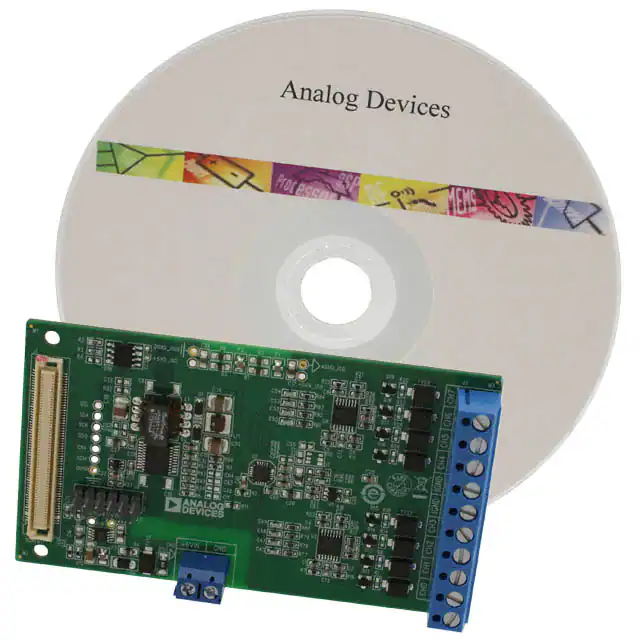
Load the evaluation software by placing the CN-0254 evaluation
software CD in the CD drive of the PC. Using My Computer,
locate the drive that contains the evaluation software CD and
open the Readme file. Follow the instructions contained in the
Readme file for installing and using the evaluation software.
Functional Block Diagram
Figure 6 shows a functional block diagram of the test setup. The
EVAL-CN0254-SDPZ-PADSSchematic pdf file contains the
detailed circuit schematics for the CN-0254 evaluation board.
The CN-0254 Design Support Package including schematics,
PCB layout, BOM, and Gerber files can be downloaded at:
http://www.analog.com/CN0254-DesignSupport.
DC POWER
SUPPLY
+
PC
USB
J1
CH0
.
.
.
CH7
120
GND
EVAL-CN0254-SDPZ
Figure 6. Evaluation Test Setup
CN0254 Design Support Package:
http://www.analog.com/CN0254-DesignSupport
Lewis Smith and D.H. Sheingold, Noise and Operational
Amplifier Circuits, Application Note AN-358, Analog
Devices.
Martin Murnane, Chris Augusta. Understanding PulSAR ADC
Support Circuitry, Application Note AN-931, Analog
Devices.
MT-031 Tutorial, Grounding Data Converters and Solving the
Mystery of “AGND” and “DGND”, Analog Devices.
MT-047 Tutorial, Op Amp Noise, Analog Devices.
MT-048 Tutorial, Op Amp Noise Relationships: 1/f Noise, RMS
Noise,and Equivalent Noise Bandwidth, Analog Devices.
10379-006
CN2
EVAL-SDP-CB1Z
SIGNAL
GENERATOR
GND
CON A OR CON B
J2
LEARN MORE
Ardizzoni, John. A Practical Guide to High-Speed PrintedCircuit-Board Layout, Analog Dialogue 39-09, September
2005.
–
+6VIN
After setting up the power supply and connecting it to the
EVAL-CN0254-SDPZ circuit board, launch the evaluation
software. Click Connect so that the software can communicate
with the SDP board. The SDP board can be used to send,
receive, and capture serial data from the EVAL-CN0254-SDPZ
board. The data in this circuit note was generated using a B&K
sign generator, Type 1051. Information regarding the SDP
board can be found at: www.analog.com/SDP.
MT-049 Tutorial, Op Amp Total Output Noise Calculations for
Single-Pole System, Analog Devices
MT-101 Tutorial, Decoupling Techniques, Analog Devices.
CN0225 Circuit Note, High Impedance, High CMR, ±10 V
Analog Front End Signal Conditioner for Industrial Process
Control and Automation, Analog Devices
CN0261 Circuit Note, Optimizing AC Performance in an 18-Bit,
250 kSPS, PulSAR Measurement Circuit, Analog Devices.
UG-197 User Guide, iCoupler ADuM347x Quad-Channel
Isolators with Integrated Transformer Driver Evaluation
Board, Analog Devices.
Rev. B | Page 5 of 6
�CN-0254
Circuit Note
Data Sheets and Evaluation Boards
CN-0254 Circuit Evaluation Board (EVAL-CN0254-SDPZ)
System Demonstration Platform (EVAL-SDP-CB1Z)
AD7689 Data Sheet and Evaluation Board
AD8608 Data Sheet and Evaluation Board
AD8605 Data Sheet and Evaluation Board
ADuM3471 Data Sheet and Evaluation Board
REVISION HISTORY
12/13—Rev. A to Rev. B
Changes to Title ................................................................................ 1
5/12—Rev. 0 to Rev. A
Changes to Figure 1 .......................................................................... 1
4/12—Revision 0: Initial Version
(Continued from first page) Circuits from the Lab reference designs are intended only for use with Analog Devices products and are the intellectual property of Analog Devices or its licensors.
While you may use the Circuits from the Lab reference designs in the design of your product, no other license is granted by implication or otherwise under any patents or other intellectual
property by application or use of the Circuits from the Lab reference designs. Information furnished by Analog Devices is believed to be accurate and reliable. However, Circuits from the
Lab reference designs are supplied "as is" and without warranties of any kind, express, implied, or statutory including, but not limited to, any implied warranty of merchantability,
noninfringement or fitness for a particular purpose and no responsibility is assumed by Analog Devices for their use, nor for any infringements of patents or other rights of third parties
that may result from their use. Analog Devices reserves the right to change any Circuits from the Lab reference designs at any time without notice but is under no obligation to do so.
©2012–2013 Analog Devices, Inc. All rights reserved. Trademarks and
registered trademarks are the property of their respective owners.
CN10379-0-12/13(B)
Rev. B | Page 6 of 6
�


 工商网监
湘ICP备2023018690号
工商网监
湘ICP备2023018690号
