Circuit Note
CN-0204
Devices Connected/Referenced
AD5751
Circuits from the Lab™ reference circuits are engineered and
tested for quick and easy system integration to help solve today’s
analog, mixed-signal, and RF design challenges. For more
information and/or support, visit www.analog.com/CN0204.
AD5662
ADR444
ADuM5401
ADuM1301
High Voltage Industrial Current/Voltage
Output Driver with Programmable Ranges
16-Bit nanoDAC® Digital-to-Analog
Converter in SOT-23
Ultralow Noise, 4.096V LDO XFET Voltage
Reference with Current Sink and Source
Quad-Channel Isolator with Integrated
DC-to-DC Converter
Triple-Channel Digital Isolator
Flexible, High Voltage, High Accuracy, Low Drift PLC/DCS Analog Output Module
The AD5662 low power (0.75 mW typical @ 5 V), rail-to-rail
output, 16-bit nanoDAC® device and the AD5751 industrial
current/voltage output driver are well matched with respect to
input and output voltage ranges, as well as reference voltage
requirements.
EVALUATION AND DESIGN SUPPORT
Circuit Evaluation Boards
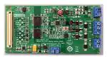
CN-0204 Circuit Evaluation Board (EVAL-CN0204-SDPZ)
System Demonstration Platform (EVAL-SDP-CB1Z)
Design and Integration Files
Schematics, Layout Files, Bill of Materials
The ADR444, with low drift (3 ppm/℃ maximum for B grade),
high initial accuracy (0.04% maximum for B grade), and low
noise (1.8 µV p-p typical, 0.1 Hz to 10 Hz), provides the
reference voltage for both the AD5751 and AD5662 and
guarantees ultralow noise, high accuracy, and low temperature
drift for the circuit. This circuit provides all the typical voltage
CIRCUIT FUNCTION AND BENEFITS
The circuit, shown in Figure 1, provides a full function, high
voltage (up to 44 V), flexible, programmable analog output
solution that meets most requirements for programmable
logic controller (PLC) and distributed control system (DCS)
applications.
+V_ISO
VDD1
GND1
SCLK
VIA
VIB
VOC
NC
VE1
GND1
SDIN
SDO
VDD2
GND2
VOA
10µF
0.1µF
VDD1
GND1
VIA
VIB
VIC
VOD
RCOUT
GND1
VIN
0.1µF
0.1µF
0.1µF
10µF
VREF VDD
SYNC
SCLK AD5662
VE2
GND2
VDD2
0.1µF
GND2
VOA
VOB
VOC
VID
VSEL
GND2
4.096V
VOUT
GND
VOB
VIC
NC
ADuM5401
SYNC1
SYNC2
CLR
FAULT
ADR444
ADuM1301
0.1µF
0V TO 4.096V
VFB
0.1µF
0.1µF
0.1µF
10µF
VOUT
DIN
+5V_ISO
10µF
GND
VREF DVCC AVDD
VOUT
VIN
SCLK
SDIN
SDO
SYNC
CLEAR
FAULT
AD5751
IOUT
GND
GND_ISO
0V TO
0V TO
0V TO
0V TO
0V TO
0V TO
5V
6V
10V
12V
40V
44V
4mA TO 20mA
0mA TO 20mA
0mA TO 24mA
09736-001
+5V
+12V TO +55V
SEE TEXT
Figure 1. Basic Analog Output Circuit for Single Channel (Simplified Schematic, All Connections and Protection Circuits Not Shown)
Rev.0
Circuits from the Lab™ circuits from Analog Devices have been designed and built by Analog Devices
engineers. Standard engineering practices have been employed in the design and construction of
each circuit, and their function and performance have been tested and verified in a lab environment at
room temperature. However, you are solely responsible for testing the circuit and determining its
suitability and applicability for your use and application. Accordingly, in no event shall Analog Devices
be liable for direct, indirect, special, incidental, consequential or punitive damages due to any cause
whatsoever connected to the use of any Circuits from the Lab circuits. (Continued on last page)
One Technology Way, P.O. Box 9106, Norwood, MA 02062-9106, U.S.A.
Tel: 781.329.4700
www.analog.com
Fax: 781.461.3113
©2011 Analog Devices, Inc. All rights reserved.
�CN-0204
Circuit Note
and current output ranges with 16-bit resolution and no
missing codes, 0.05% linearity, and less than 0.2% total output
error.
The ADuM1301 and ADuM5401 provide all the necessary
signal isolation between the microcontroller and the analog
signal chain. The ADuM5401 also provides isolated 5 V power.
The circuit also contains key features for industrial applications,
such as on-chip output fault detection, CRC checking to prevent
packet error (PEC), and flexible power-up options, making it an
ideal choice for robust industrial control systems. No external
precision resistors or calibration routines are needed to
maintain consistent performance in mass production, thereby
making it ideal for PLC or DCS modules.
CIRCUIT DESCRIPTION
The AD5751 is a single channel, low cost, precision voltage/
current output driver developed to meet the requirements of
industrial process control applications. The AD5751 is specified
to operate with a power supply range from 10.8 V to 55 V, and
the voltage output can be up to 44 V. The voltage output range
can be programmed for the standard output ranges and 20%
overrange settings for PLC and DCS applications: 0 V to 5 V,
0 V to 10 V, 0 V to 6 V, 0 V to 12 V. In addition, two high voltage
output ranges are also provided: 0 V to 40 V and 0 V to 44 V.
The current output, which is provided on a separate pin, can be
programmed for the standard ranges of 4 mA to 20 mA, 0 mA
to 20 mA, 0 mA to 24 mA. There is also a 2% overrange setting
which provides 3.92 mA to 20.4 mA, 0 mA to 20.4 mA, and
0 mA to 24.5 mA. The voltage and current output pins can be
tied together to configure the end system as a single-channel
output if desired.
The AD5662 is a single channel, low cost, low power, rail-to-rail
voltage buffered output nanoDAC device. The AD5662
guarantees ±1 LSB DNL under a wide range of reference
voltages that can vary from 0.75 V to the VDD supply. In the
circuit of Figure 1, the AD5751 and AD5662 operate from a
common reference source of 4.096 V, provided by the ADR444.
The whole system will benefit from the ultralow noise and low
temperature coefficient of the ADR444. The ADR44x family of
references are ideal for driving either the reference or the power
input of converters because they can source and sink current.
The AD5662 also incorporates a power-on reset circuit to
ensure that the DAC output powers up to either midscale or
zero and remains there until a valid write takes place.
The ADuM1301 is a triple channel digital isolator. The
ADuM5401 is a quad channel digital isolator with isoPower®
integrated, isolated, dc-to-dc converter. They are both based on
the iCoupler® technology. They are used to provide isolation
between the signal chain and the system microcontroller, with
an isolation rating of 2.5 kV rms. The ADuM5401 provides an
isolated 5 V power supply for all the circuit in the secondary
side.
The digital power and analog power should be separated and
connected with a ferrite bead. Each power is well decoupled by
a 10 µF paralleled with a 0.1 µF ceramic capacitor. See the
schematics in the CN0204 Design Support package for more
details.
Devices for PLC and DCS applications generally need ESD
protection and overvoltage protection much higher than the
formal recommended specifications. The AD5751 has
integrated ESD protection diodes internal to each pin that can
prevent damage from transients. However, the industrial
control environment can subject I/O circuits to much higher
transients. External 64 V, 1500 W transient voltage suppressors
(TVS); a 50 mA, 30 V PolySwitch; and power Schottky diodes
are built into the EVAL-CN0204-SDPZ circuit board to provide
higher voltage ESD protection, 50 mA overcurrent, and 64 V
overvoltage protection. The optional external protection
circuits are not shown in the simplified schematic of Figure 1
but can be found in the detailed schematic (EVAL-CN0204SDPZ-SCH pdf file) in the CN0204 Design Support package:
www.analog.com/CN0204-DesignSupport.
The circuit must be constructed on a multilayer PC board with
a large area ground plane. Proper layout, grounding, and
decoupling techniques must be used to achieve optimum
performance (see Tutorial MT-031, Grounding Data Converters
and Solving the Mystery of "AGND" and "DGND," and Tutorial
MT-101, Decoupling Techniques).
Measurements
Integral nonlinearity (INL), differential nonlinearity (DNL),
and output error are the most important specifications for PLC,
DCS, and other process control systems. The AD5751 has
highly flexible and configurable output ranges that can be
tailored to meet the needs of the application. Measurements of
INL, DNL, and output error for the circuit are shown in Figure 2,
Figure 3, and Figure 4, respectively. This data was taken at 25°C
in the voltage output mode using the internal current sense
resistor. The AD5751 range was set for 0 V to 5 V. The test
results for all the other ranges are listed in Table 1.
Rev. 0 | Page 2 of 6
�Circuit Note
CN-0204
0.3
The test results shown in Table 1 were made at 25°C using the
EVAL-CN0204-SDPZ board powered by an Agilent E3631A dc
supply and measured with an Agilent 34401A digital multimeter.
0.2
DNL (LSB)
0.1
Note that the output ranges 0 mA to 20.4 mA and 0 mA to
24.5 mA are both designed to be trimmed by the customer to
precisely match the 0 mA to 20 mA and 0 mA to 24 mA ranges.
The 1.70% FSR output error measurement in the 0 mA to 20.4 mA
range includes the gain error, which can be removed by
customer calibration.
0
–0.1
09736-003
–0.2
57344
61440
65536
61440
65536
53248
57344
49152
45056
40960
36864
32768
28672
24576
20480
16384
8192
12288
4096
0
–0.3
DAC CODE
Figure 3. DNL for 0 V to 5 V Output Range
10
–0.04
–0.05
OUTPUT ERROR (%FSR)
0
–5
–10
–0.07
–0.08
09736-004
09736-002
–0.09
53248
49152
45056
40960
36864
32768
28672
24576
20480
16384
8192
0
12288
–0.10
65536
61440
57344
53248
49152
45056
40960
36864
32768
28672
24576
20480
16384
8192
12288
0
4096
–15
–0.06
4096
INL (LSB)
5
DAC CODE
DAC CODE
Figure 2. INL for 0 V to 5 V Output Range
Figure 4. Output Error for 0 V to 5 V Output Range
Table 1. Test Results for All Output Ranges
Range
Current Sense Resistor
INL (LSB)
Linearity (%FSR)
Ouptut Error (%FSR)
0 V to 5 V
Don't Care
10.8
0.017
0.09
0 V to 10 V
Don't Care
9.9
0.015
0.08
0 V to 6 V
Don't Care
10.5
0.016
0.09
0 V to 12 V
Don't Care
9.2
0.014
0.08
0 V to 40 V
Don't Care
10.1
0.015
0.06
0 V to 44 V
Don't Care
9.5
0.015
0.20
4 mA to 20 mA
Internal
8.5
0.016
0.04
4 mA to 20 mA
External
8.4
0.013
0.04
0 mA to 20 mA
Internal
9.8
0.015
0.05
0 mA to 20 mA
External
8.9
0.014
0.05
0 mA to 24 mA
Internal
8.4
0.013
0.05
0 mA to 24 mA
External
12.0
0.018
0.05
3.92 mA to 20.4 mA
Internal
11.8
0.053
0.80
0 mA to 20.4 mA
Internal
9.4
0.014
1.70
0 mA to 24.5 mA
Internal
12.4
0.019
1.50
Rev. 0 | Page 3 of 6
�CN-0204
Circuit Note
Getting Started
Load the evaluation software by placing the CN0204 Evaluation
Software disc in the CD drive of the PC. Using "My Computer,"
locate the drive that contains the evaluation software disc and
open the Readme file. Follow the instructions contained in the
Readme file for installing and using the evaluation software.
COMMON VARIATIONS
This circuit describes one implementation of a family of driver
and DAC products, from which various devices can be selected
to achieve desired performance. Resolution of 12 bits to 16 bits
with 0.1% accuracy are typical requirements for PLC and DCS
applications. For applications not requiring 16-bit resolution,
the AD5620 (12-bit) and AD5640 (14-bit) are available, and
have internal references.
Functional Block Diagram
Figure 5 shows a functional block diagram of the test setup. The
pdf file “EVAL-CN0204-SDPZ-SCH” contains the detailed
circuit schematics for the CN0204 evaluation board. This file
is contained in the CN-0204 Design Support Package:
www.analog.com/CN0204-DesignSupport.
For multichannel applications, the AD5623R (12-bit), AD5643R
(14-bit), and AD5663R (16-bit) are dual nanoDAC devices,
and the AD5624R (12-bit), AD5644R (14-bit), and AD5664R
(16-bit) are quad nanoDAC devices.
Setup
The AD5750-1 and AD5750 are both bipolar analog output
drivers and can supply ±10 V and ±20 mA.
Connect the 120-pin connector on the EVAL-CN0204-SDPZ
circuit board to the connector marked “CON A” or “CON B” on
the EVAL-SDP-CB1Z evaluation (SDP) board. Nylon hardware
should be used to firmly secure the two boards, using the
holes provided at the ends of the 120-pin connectors. After
setting the dc output supply to +25 V, −25 V and +6 V output,
turn the power supply off.
CIRCUIT EVALUATION AND TEST
Equipment Needed (Equivalents Can Be Substituted)
• System Demonstration Platform (EVAL-SDP-CB1Z)
• CN-0204 Circuit Evaluation Board (EVAL-CN0204-SDPZ)
• CN-0204 Evaluation Software
The Agilent E3631A supply has ±25 V/1 A and 6 V/5 A output
channels. The ±25 V/1 A and 6 V/5 A are isolated with respect
to each other. Therefore, the ±25 V/1 A can be used to provide
the +50 V power supply to the circuit. There must be no
external connection between the “−” terminal of the 6 V/5 A
supply and the “COM” terminal of the ±25 V/1 A supply.
• Software for controlling external test measurement
equipment (not included on CD)
• Agilent 34401A, 6.5 Digit Digital Multimeter
• Agilent E3631A 0 V to 6 V/5 A; ±25 V/1 A triple output dc
power supply
With power to the supply off, connect a +25 V power supply to
the pin of CN3 marked “12~50VIN,” and the −25 V power supply
to the pin of CN3 marked “GND_ISO.” Leave the “COM” of
• National Instruments GPIB to USB-B interface and cable
AGILENT E3631A
TRIPLE POWER SUPPLY
AGILENT
34401A
MULTIMETER
–
12V TO 50V GND_ISO
ISO
+
–
GND
+6V
CN2
CN3
CN1
OR
CN4
GPIB
VOUT
OR
IOUT
120 PIN SDP
EVAL-CN0204-SDPZ
GND
6V
OUT
+
±25V
COM
Figure 5. Test Setup Functional Block Diagram
Rev. 0 | Page 4 of 6
USB
PC
USB
USB
SDP
CON A
OR
CON B
09736-005
• PC (Windows® 2000 or Windows XP) with USB interface
�Circuit Note
CN-0204
Table 2. Jumper Settings for EVAL-CN0204-SDPZ (Bold Values Are Default Settings)
Jumper
Descriptions
JP1
Sets the address of
AD5751
JP2
Sets the external
compensation capacitor
JP3
VSENSE+ Setting
JP4
Sets the CLEAR Mode for
AD5751
JP5
Shorts the VOUT and IOUT
pins
Setting
Function
Shorting Pin1 with Pin2
Address of AD5751 : b'001
Shorting Pin3 with Pin2
Address of AD5751 : b'000
Shorting
Adding 1 nF Compensation Capacitor
Opening
Removing 1 nF Compensation Capacitor
Shorting
Shorting VSENSE+ with VOUT internally
Opening
VSENSE+ has no connection with VOUT internally
Shorting
Clears to midscale
Opening
Clears to zero scale
Shorting
Shorts VOUT and IOUT together.
Opening
VOUT and IOUT have no connection internally
±25 V/1 A unconnected. Connect +6 V to CN2 the same way.
Turn on the power supply and then connect the USB cable with the
SDP board to the USB port on the PC. Note: Do not connect the
USB cable to the mini USB connector on the SDP board before
turning on the dc power supply for the EVAL-CN0204-SDPZ.
Test
After setting up the test equipment, connect the pin of CN4
marked “VOUT” or the pin of CN1 marked “IOUT” to the
input of the Agilent 34401A. Make sure that the cable
connection on the front panel of the Agilent 34401A is correct,
depending on the different input signal type (current or
voltage). Testing the INL, DNL, and total error will take a
considerable amount of time because all of the AD5662 16-bit
DAC levels must be set and measured by the 34401A.
The software provided on the CD allows the DAC codes to be
set by the PC. An automatic test program is necessary to step
through the codes and analyze the data. This is not provided on
the CD but must be implemented by the customer to
correspond to the requirements of the particular multimeter
used in the test setup.
In the test configuration shown in Figure 5, the GPIB output of
the 34401A multimeter interfaces to a second USB port on the
PC using the National Instruments GPIB to USB-B interface
and cable. This allows the multimeter readings corresponding
to each code to be loaded into an Excel spreadsheet on the PC.
The data is then analyzed for INL, DNL, and total error using
industry-standard definitions.
For more details on the definitions and how to calculate the
INL, DNL, and total error from the measured data, see the
"TERMINOLOGY" section of the AD5662 data sheet and also
the following reference: Data Conversion Handbook, "Testing
Data Converters," Chapter 5, Analog Devices.
LEARN MORE
CN-0204 Design Support Package:
www.analog.com/CN0204-DesignSupport
Slattery, Colm, Derrick Hartmann, and Li Ke, "PLC Evaluation
Board Simplifies Design of Industrial Process Control
Systems.” Analog Dialogue (April 2009).
CN-0063 Circuit Note, 16-Bit Fully Isolated Voltage Output
Module Using the AD5662 DAC, ADuM1401 Digital Isolator,
and External Amplifiers, Analog Devices.
CN-0064 Circuit Note, 16-Bit Fully Isolated 4 mA to 20 mA
Output Module Using the AD5662 DAC, ADuM1401 Digital
Isolator, and External Amplifiers, Analog Devices.
CN-0065 Circuit Note, 16-Bit Fully Isolated Output Module
Using the AD5422 Single Chip Voltage and Current Output
DAC and the ADuM1401 Digital Isolator, Analog Devices.
CN-0066 Circuit Note, Fully Isolated Input Module Based on the
AD7793 24-Bit Σ-Δ ADC and the ADuM5401 Digital Isolator,
Analog Devices.
CN-0067 Circuit Note, Fully Isolated Input Module Based on the
AD7793 24-Bit Σ-Δ ADC, the ADuM5401 Digital Isolator,
and a High Performance In-Amp, Analog Devices.
CN-0097 Circuit Note, Simplified 12-Bit Voltage and 4 mA-to20 mA Output Solution Using the AD5412, Analog Devices.
CN-0209 Circuit Note, Fully Programmable Universal Analog
Front End for Process Control Applications, Analog Devices.
AN-0971 Application Note, Recommendations for Control of
Radiated Emissions with isoPower Devices, Mark Cantrell.
MT-031 Tutorial, Grounding Data Converters and Solving the
Mystery of “AGND” and “DGND”, Analog Devices.
MT-101 Tutorial, Decoupling Techniques, Analog Devices.
Rev. 0 | Page 5 of 6
�CN-0204
Circuit Note
Kester, Walt. Practical Design Techniques for Sensor Signal
Conditioning, Analog Devices, 1999, ISBN 0-916550-20-6
Kester, Walt. Data Conversion Handbook, Chapter 5, Analog
Devices.
Data Sheets and Evaluation Boards
CN-0204 Circuit Evaluation Board (EVAL-CN0204-SDPZ)
System Demonstration Platform (EVAL-SDP-CB1Z)
AD5751 Data Sheet
AD5751 Evaluation Board
AD5662 Data Sheet
AD5662 Evaluation Board
REVISION HISTORY
10/11—Revision 0: Initial Version
Continued from first page) Circuits from the Lab circuits are intended only for use with Analog Devices products and are the intellectual property of Analog Devices or its licensors. While you
may use the Circuits from the Lab circuits in the design of your product, no other license is granted by implication or otherwise under any patents or other intellectual property by
application or use of the Circuits from the Lab circuits. Information furnished by Analog Devices is believed to be accurate and reliable. However, "Circuits from the Lab" are supplied "as is"
and without warranties of any kind, express, implied, or statutory including, but not limited to, any implied warranty of merchantability, noninfringement or fitness for a particular
purpose and no responsibility is assumed by Analog Devices for their use, nor for any infringements of patents or other rights of third parties that may result from their use. Analog Devices
reserves the right to change any Circuits from the Lab circuits at any time without notice but is under no obligation to do so.
©2011 Analog Devices, Inc. All rights reserved. Trademarks and
registered trademarks are the property of their respective owners.
CN09736-0-10/11(0)
Rev. 0 | Page 6 of 6
�


 工商网监
湘ICP备2023018690号
工商网监
湘ICP备2023018690号
