APT10M11JVRU2
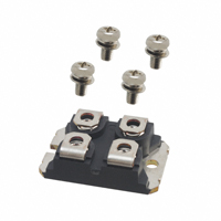
ISOTOP® Boost chopper MOSFET Power Module
K
VDSS = 100V RDSon = 11mΩ max @ Tj = 25°C ID = 142A @ Tc = 25°C
Applicatio n • AC and DC motor control • Switched Mode Power Supplies • Power Factor Correction • Brake switch Features • Power MOS V® MOSFETs - Low RDSon - Low input and Miller capacitance - Low gate charge - Fast intrinsic diode - Avalanche energy rated - Very rugged • ISOTOP® Package (SOT-227) • Very low stray inductance • High level of integration Benefits • Outstanding performance at high frequency operation • Direct mounting to heatsink (isolated package) • Low junction to case thermal resistance • Very rugged • Low profile
D
G
S
S G D
K
ISOTOP
Absolute maximum ratings
Symbol VDSS ID IDM VGS RDSon PD IAR EAR EAS IFA V IFRMS
Parameter Drain - Source Breakdown Voltage Continuous Drain Current Pulsed Drain current Gate - Source Voltage Drain - Source ON Resistance Maximum Power Dissipation Avalanche current (repetitive and non repetitive) Repetitive Avalanche Energy Single Pulse Avalanche Energy Maximum Average Forward Current Duty cycle=0.5 RMS Forward Current (Square wave, 50% duty) Tc = 25°C Tc = 80°C
Tc = 25°C
mJ A
Tc = 90°C
These Devices are sensitive to Electrostatic Discharge. Proper Handing Procedures Should Be Followed.
APT website – http://www.advancedpower.com
1–7
APT10M11JVRU2 – Rev 0 October, 2004
Max ratings 100 142 106 576 ±30 11 450 144 50 2500 30 47
Unit V A V mΩ W A
�APT10M11JVRU2
All ratings @ Tj = 25°C unless otherwise specified Electrical Characteristics
Symbol B VDSS IDSS RDS(on) VGS(th) IGSS Characteristic Drain - Source Breakdown Voltage Zero Gate Voltage Drain Current Drain – Source on Resistance Gate Threshold Voltage Gate – Source Leakage Current Test Conditions VGS = 0 V, ID = 250µA
VGS = 0V,VDS = 100V VGS = 0V,VDS = 80V
Min 100 Tj = 25°C Tj = 125°C 2
Typ
Max 250 1000 11 4 ±100
Unit V µA mΩ V nA
VGS = 10V, ID = 71A VGS = VDS, ID = 2.5mA VGS = ±20 V, VDS = 0 V
Dynamic Characteristics
Symbol Ciss Coss Crss Qg Qgs Qgd Td(on) Tr Td(off) Tf
Characteristic Input Capacitance Output Capacitance Reverse Transfer Capacitance Total gate Charge Gate – Source Charge Gate – Drain Charge Turn-on Delay Time Rise Time Turn-off Delay Time Fall Time
Test Conditions VGS = 0 V VDS = 25V f = 1MHz VGS = 10V VBus = 50V ID = 50A @ TJ=25°C VGS = 15V VBus = 50V ID = 142A @ TJ=25°C R G = 0.6Ω
Min
Typ 8600 3200 1180 300 95 110 16 48 51 9
Max
Unit pF
nC
ns
Diode ratings and characteristics
Symbol VF IRM CT trr Reverse Recovery Time IRRM Qrr trr Qrr IRRM Maximum Reverse Recovery Current Reverse Recovery Charge Reverse Recovery Time Reverse Recovery Charge Maximum Reverse Recovery Current Characteristic Diode Forward Voltage Maximum Reverse Leakage Current Junction Capacitance Reverse Recovery Time
Test Conditions IF = 30A IF = 60A IF = 30A VR = 200V VR = 200V VR = 200V IF=1A,VR=30V di/dt =200A/µs IF = 30A VR = 133V di/dt =200A/µs
Min
Tj = 125°C Tj = 25°C Tj = 125°C Tj = 25°C Tj = 25°C Tj = 125°C Tj = 25°C Tj = 125°C Tj = 25°C Tj = 125°C Tj = 125°C
Typ 1.1 1.4 0.9 94 21 24 48 3 6 33 150 31 335 19
Max 1.15 250 500
Unit V µA pF ns
A nC ns nC A
IF = 30A VR = 133V di/dt =1000A/µs
APT website – http://www.advancedpower.com
2–7
APT10M11JVRU2 – Rev 0 October, 2004
�APT10M11JVRU2
Thermal and package characteristics
Symbol RthJC RthJA VISOL TJ,TSTG TL Torque Wt Characteristic Junction to Case Junction to Ambient (IGBT & Diode)
RMS Isolation Voltage, any terminal to case t =1 min, I isol
很抱歉,暂时无法提供与“APT10M11JVRU2”相匹配的价格&库存,您可以联系我们找货
免费人工找货