AOZ1331ADI
Dual Channel Smart Load Switch
General Description
Features
The AOZ1331ADI is a dual channel load switch with typical 20mΩ on-resistance in a small package. It contains two
n-channel MOSFETs for up to 5.5V input voltage operation and 6A current each channel with 2.5V to 5V bias
supply. Each load switch is independently controlled by a
low voltage control signal through ON1/ON2 pin.
0.8V to 5.5V input voltage range
6A continuous current per channel
Low RDS(ON) internal NFETs
The AOZ1331ADI integrates an internal 250Ω load resistor in each channel for quick output discharge when load
switch is off. The optional external capacitor connected
CT1/CT2 for output slew rate control.
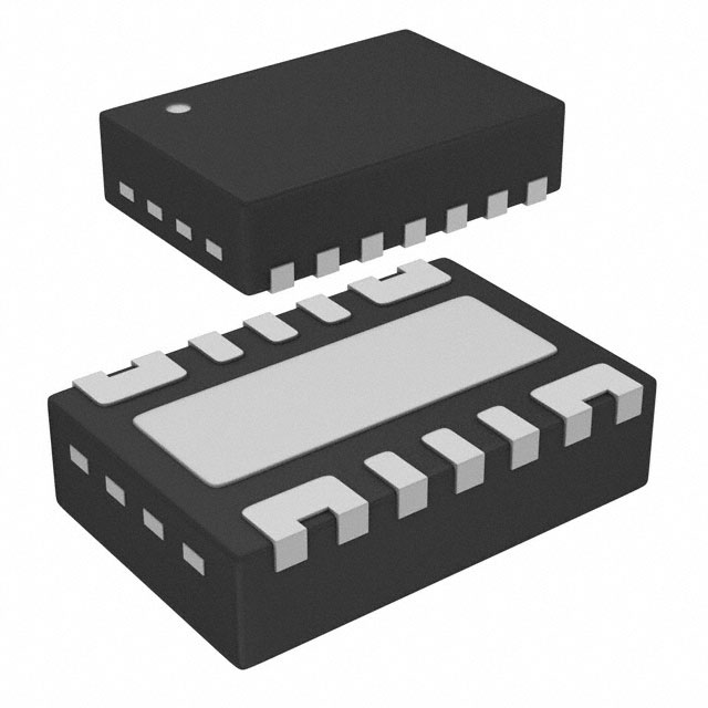
The AOZ1331ADI is available in a 3mm x 2mm DFN-14L
package with bottom thermal pad and is rated over a
-40°C to +85°C ambient temperature range.
– 20mΩ at VBIAS = 5V
Low quiescent current
– 80µA (both channels)
– 60µA (single channel)
Adjustable rise time
2.5V to 5V bias voltage
Integrated quick output discharge resistor
Thermally enhanced 3mm x 2mm DFN-14L package
Applications
Portable computers
Ultrabooks
Tablet PC
Set top boxes
LCD TVs
Telecom/Networking/Datacom
SSD
Consumer electronics
Typical Application
VIN1
VOUT1
OUT1
IN1
CIN1
CL1
ON
ON1
OFF
CT1
AOZ1331ADI
VBIAS
CT1
GND
CT2
ON
ON2
CT2
OFF
IN2
VIN2
Rev. 1.3 July 2018
VOUT2
OUT2
CIN1
CL2
www.aosmd.com
Page 1 of 14
�AOZ1331ADI
Ordering Information
Part Number
Temperature Range
Package
Environmental
AOZ1331ADI
-40°C to +85°C
3mm x 2mm DFN-14L
Green
All AOS products are offered in packages with Pb-free plating and compliant to RoHS standards.
Please visit www.aosmd.com/media/AOSGreenPolicy.pdf for additional information.
Pin Configuration
IN1
1
14
OUT1
IN1
2
13
OUT1
ON1
3
12
CT1
VBIAS
4
11
GND
ON2
5
10
CT2
IN2
6
IN2
7
EPAD
9
OUT2
8
OUT2
3mm x 2mm DFN-14
(Top View)
Pin Description
Pin Number
Pin Name
Pin Function
1, 2
IN1
Switch 1 Input. Bypass capacitor is recommended to minimize input voltage dip.
3
ON1
Enable Input of Switch 1. Switch 1 is on when ON1 is pulled high, and is off when ON1 is
pulled low. Do not leave floating.
4
VBIAS
Bias Voltage. Power supply to this device. Recommended voltage range is 2.5V to 5.5V.
5
ON2
Enable Input of Switch 2. Switch 2 is on when ON2 is pulled high, and is off when ON2 is
pulled low. Do not leave floating.
6, 7
IN2
Switch 2 Input. Bypass capacitor is recommended to minimize input voltage dip.
8, 9
OUT2
Switch 2 Output.
10
CT2
Slew rate control of switch 2.
11
GND
Ground.
12
CT1
Slew rate control of switch 1.
13, 14
OUT1
EPAD
Exposed Pad
Rev. 1.3 July 2018
Switch 1 Output.
The exposed bottom pad must be connected to GND.
www.aosmd.com
Page 2 of 14
�AOZ1331ADI
Functional Block Diagram
IN1
CT1
ON1
VBIAS
ON2
Control
Logic
OUT1
Charge Pump
GND
Control
Logic
OUT2
CT2
IN2
Rev. 1.3 July 2018
www.aosmd.com
Page 3 of 14
�AOZ1331ADI
Absolute Maximum Ratings
Recommend Operating Ratings
Exceeding the Absolute Maximum ratings may damage the
device.
The device is not guaranteed to operate beyond the Maximum
Operating Ratings.
Parameter
Rating
Parameter
IN1, IN2, VBIAS, ON1, ON2 to GND
-0.3V to 6V
Supply Voltage (VIN)
OUT1, OUT2 to GND
-0.3V to 6V
Ambient Temperature (TA)
Junction Temperature (TJ)
+150°C
Storage Temperature (TS)
-65°C to +150°C
ESD Rating HBM/CDM
2kV/1kV
Rating
5.5V
-40°C to +85°C
Package Thermal Resistance
3x2 DFN-14 (JC)
3x2 DFN-14 (JA)
10°C/W
65°C/W
Electrical Characteristics
TA = 25°C, VBIAS = 5V, unless otherwise specified. Specifications in BOLD indicate a temperature range of -40°C to +85°C.
Symbol
Parameter
Conditions
Min.
Typ.
Units
5.5
V
5.5
V
VINX
IN Supply Voltage
VBIAS
VBIAS Supply Voltage
ID1, 2
Maximum Continuous Current
VINX = VONX = 5V
6
A
Maximum Pulsed Switch Current
VINX = VONX = 5V
Pulse < 300µs, 2% Duty Cycle
8
A
Iq2
Quiescent Supply Current of VBIAS
(Two Channels)
IOUT1 = IOUT2 = 0V,
VIN1,2 = VON1,2 = 5V
80
Iq1
Quiescent Supply Current of VBIAS
(Single Channel)
IOUT1 = IOUT2 = 0V,
VIN1,2 = VON1 = 5V, VON2 = 0V
60
VBIAS Shutdown Supply Current
VON1,2 = 0V, VOUT1,2 = 0V
IPLS1, 2
IOFF
IINOFF
IN1, IN2 Shutdown Supply Current
(Single Channel)
0.8
Max.
2.5
1
2
2.1
8
VONX = 0V, VOUTX = 0V,
VINX = 3.3V
0.3
3
VONX = 0V, VOUTX = 0V,
VINX = 1.8V
0.07
2
VONX = 0V, VOUTX = 0V,
VINX = 0.8V
0.04
1
VON1,2 = 5V
VONH1, 2
ON1, 2 High Level Voltage
VINX = 0.8V to 5V
VONL1, 2
ON1, 2 Low Level Voltage
VINX = 0.8V to 5V
µA
µA
VONX = 0V, VOUTX = 0V,
VINX = 5V
ON1, 2 Leakage Current
ION1, 2
120
1
1.2
µA
µA
µA
V
0.5
V
Switching ON Resistance
RON
Switch ON-State Resistance
IOUTX = -200mA
VINX = 0.8V to 5V
20
25
mΩ
RPD
Output Pull-Down Resistance
IOUTX = 15mA
VINX = 5V, VONX = 0V
250
300
Ω
Rev. 1.3 July 2018
www.aosmd.com
Page 4 of 14
�AOZ1331ADI
Switching Characteristics
VON
50%
50% t
OFF
tON
90%
VOUT
90%
tD-ON
50%
50%
10%
1%
tR
10%
tF
Test conditions: TA = 25°C, CINX = 1µF, CTX = 1nF, CLX = 0.1µF, RLX = 10Ω (unless otherwise specified).
Symbol
Parameter
Min.
Typ.
Max.
Units
VINX = 5V, VBIAS = VONX = 5V
Turn-ON Time
1467
tD-ON
Turn-ON Delay time
350
tR
Turn-ON Rise Time
1705
Turn-OFF Time
5.83
Turn-OFF Fall Time
3.57
tON
tOFF
tF
µs
VINX = 0.8V, VBIAS = VONX = 5V
Turn-ON Time
582
tD-ON
Turn-ON Delay time
329
tR
Turn-ON Rise Time
350
Turn-OFF Time
91.2
Turn-OFF Fall Time
13.2
tON
tOFF
tF
µs
VINX = 2.5V, VBIAS = VONX = 2.5V
Turn-ON Time
2010
tD-ON
Turn-ON Delay time
446
tR
Turn-ON Rise Time
1985
Turn-OFF Time
7.46
Turn-OFF Fall Time
5.7
tON
tOFF
tF
µs
VINX = 0.8V, VBIAS = VONX = 2.5V
Turn-ON Time
1220
tD-ON
Turn-ON Delay time
664
tR
Turn-ON Rise Time
760
Turn-OFF Time
84.6
Turn-OFF Fall Time
13.2
tON
tOFF
tF
Rev. 1.3 July 2018
www.aosmd.com
µs
Page 5 of 14
�AOZ1331ADI
Typical Characteristics
Quiescent Current vs. VBIAS (Single Channel)
RDSON vs. VIN
(VINX = VBIAS = 5V, VON1 = 5V, VON2 = 0V)
(VBIAS = 5.5V, IOUT = 200mA)
100
90
23
22
-40°C
25°C
70°C
80°C
80
21
RDSON (m)
IBIAS (µA)
70
60
50
40
20
19
18
17
30
16
20
15
10
14
0
2.5
3
3.5
4.5
4
5
13
5.5
-40°C
25°C
70°C
85°C
0.8
1.8
2.8
VBIAS (V)
2.5
-40°C
25°C
70°C
80°C
2
VOUT (V)
100
IBIAS (µA)
(TA = 25°C, VIN = 2V)
(VINX = VBIAS = 5V, VON1 = 5V, VON2 = 5V)
120
80
60
1.5
1
VBIAS = 2.5V
VBIAS = 3.3V
40
VBIAS = 5V
0.5
V BIAS = 5.5V
20
0
5.8
VOUT vs. VON
Quiescent Current vs. VBIAS (Both Channels)
140
4.8
3.8
VIN (V)
2.5
3
3.5
4.5
4
5
5.5
0
0.5
VBIAS (V)
0.7
0.9
1.1
1.3
VON (V)
RDSON vs. VIN
(VBIAS = 2.5V, IOUT = 200mA)
31
29
RDSON (m)
27
25
23
21
19
-40°C
25°C
70°C
85°C
17
15
0.8
1.8
2.8
3.8
4.8
5.8
VIN (V)
Rev. 1.3 July 2018
www.aosmd.com
Page 6 of 14
�AOZ1331ADI
Typical Characteristics (Continue)
tON vs. VIN
4000
400
2500
2000
350
300
1500
250
1000
200
500
150
0
0.8
1.4
-40°C
25°C
70°C
80°C
450
tD-ON (µs)
3000
(VBIAS = 5.5V)
500
-40°C
25°C
70°C
80°C
3500
tON (µs)
tD-ON vs. VIN
(VBIAS = 2.5V)
2.0
2.6
3.2
3.8
4.4
5
100
5.6
0.8
1.4
2.0
2.6
VIN (V)
2000
1600
tON vs. VIN
tR vs. VIN
(VBIAS = 2.5V)
4500
3500
tR (µs)
tON (µs)
1200
1000
800
5
5.6
4.4
5
5.6
4.4
5
5.6
3000
2500
2000
600
1500
400
1000
200
0.8
1.4
2.0
2.6
3.2
3.8
4.4
5
500
5.6
0.8
1.4
2.0
2.6
VIN (V)
1000
3.2
3.8
VIN (V)
tD-ON vs. VIN
tR vs. VIN
(VBIAS = 2.5V)
(VBIAS = 5.5V)
1900
-40°C
25°C
70°C
80°C
900
-40°C
25°C
70°C
80°C
1700
1500
800
1300
tR (µs)
tD-ON (µs)
4.4
-40°C
25°C
70°C
80°C
4000
1400
0
3.8
(VBIAS = 5.5V)
-40°C
25°C
70°C
80°C
1800
3.2
VIN (V)
700
600
1100
900
700
500
500
400
300
300
0.8
1.4
2.0
2.6
3.2
3.8
4.4
5
5.6
100
0.8
VIN (V)
Rev. 1.3 July 2018
1.4
2.0
2.6
3.2
3.8
VIN (V)
www.aosmd.com
Page 7 of 14
�AOZ1331ADI
Typical Characteristics (Continued)
160
tOFF vs. VIN
tF vs. VIN
(VBIAS = 2.5V)
(VBIAS = 2.5V)
20
-40°C
25°C
70°C
80°C
140
18
14
100
tF (µs)
tOFF (µs)
120
80
12
10
8
60
6
40
4
20
0
-40°C
25°C
70°C
80°C
16
2
0.8
1.4
2.0
2.6
3.2
3.8
4.4
5
0
5.6
0.8
1.4
2.0
2.6
VIN (V)
160
tF vs. VIN
(VBIAS = 5.5V)
(VBIAS = 5.5V)
20
-40°C
25°C
70°C
80°C
120
4.4
5
5.6
-40°C
25°C
70°C
80°C
18
16
14
tON (µs)
tOFF (µs)
3.8
tOFF vs. VIN
140
100
80
12
10
8
60
6
40
4
20
0
3.2
VIN (V)
2
0.8
1.4
2.0
2.6
3.2
3.8
4.4
5
5.6
0
0.8
VIN (V)
Rev. 1.3 July 2018
1.4
2.0
2.6
3.2
3.8
4.4
5
5.6
VIN (V)
www.aosmd.com
Page 8 of 14
�AOZ1331ADI
Functional Characteristic
Turn-ON & Turn-ON Rise Times
Turn-ON & Turn-ON Rise Times
(VINX = 5V, VBIAS = 5V, CINX = 1µF, CTX = 1nF, CLX = 0.1µF, RLX = 10)
(VINX = 0.8V, VBIAS = 5V, CINX = 1µF, CTX = 1nF, CLX = 0.1µF, RLX = 10)
VON1
(5V/div)
VOUT1
(3V/div)
VON1
(5V/div)
VOUT1
(0.5V/div)
VON2
(5V/div)
VON2
(5V/div)
VOUT2
(3V/div)
VOUT2
(0.5V/div)
2ms/div
2ms/div
Turn-ON & Turn-ON Rise Times
Turn-ON & Turn-ON Rise Times
(VINX = 2.5V, VBIAS = 2.5V, CINX = 1µF, CTX = 1nF, CLX = 0.1µF, RLX = 10)
(VINX = 0.8V, VBIAS = 2.5V, CINX = 1µF, CTX = 1nF, CLX = 0.1µF, RLX = 10)
VON1
(5V/div)
VON1
(5V/div)
VOUT1
(2V/div)
VOUT1
(0.5V/div)
VON2
(5V/div)
VON2
(5V/div)
VOUT2
(2V/div)
VOUT2
(0.5V/div)
2ms/div
2ms/div
Turn-OFF & Turn-OFF Fall Times
Turn-OFF & Turn-OFF Fall Times
(VINX = 5V, VBIAS = 5V, CINX = 1µF, CTX = 1nF, CLX = 0.1µF, RLX = 10)
(VINX = 0.8V, VBIAS = 5V, CINX = 1µF, CTX = 1nF, CLX = 0.1µF, RLX = 10)
VON1
(5V/div)
VON1
(5V/div)
VOUT1
(3V/div)
VOUT1
(0.5V/div)
VON2
(5V/div)
VON2
(5V/div)
VOUT2
(3V/div)
VOUT2
(0.5V/div)
5µs/div
Rev. 1.3 July 2018
50µs/div
www.aosmd.com
Page 9 of 14
�AOZ1331ADI
Functional Characteristics (Continued)
Turn-OFF & Turn-OFF Fall Times
Turn-OFF & Turn-OFF Fall Times
(VINX = 2.5V, VBIAS = 2.5V, CINX = 1µF, CTX = 1nF, CLX = 0.1µF, RLX = 10)
(VINX = 0.8V, VBIAS = 2.5V, CINX = 1µF, CTX = 1nF, CLX = 0.1µF, RLX = 10)
VON1
(5V/div)
VON1
(5V/div)
VOUT1
(2V/div)
VOUT1
(0.5V/div)
VON2
(5V/div)
VON2
(5V/div)
VOUT2
(2V/div)
VOUT2
(0.5V/div)
50µs/div
50µs/div
Turn-ON & Turn-OFF @ IOUT = 6A
(VIN1 = 0.8V, VBIAS = 5V, CIN1 = 4.7µF, CT1 = 1nF, CL1 = 4.7µF)
Turn-ON & Turn-OFF @ IOUT = 6A
(VIN1 = 2.5V, VBIAS = 5V, CIN1 = 4.7µF, CT1 = 1nF, CL1 = 4.7µF)
VON
(5V/div)
VON
(5V/div)
VOUT
(2V/div)
VOUT
(1V/div)
IOUT
(2A/div)
IOUT
(2A/div)
10ms/div
Rev. 1.3 July 2018
10ms/div
www.aosmd.com
Page 10 of 14
�AOZ1331ADI
Detailed Description
Applications Information
ON/OFF Control
The basic AOZ1331ADI application circuit is shown in the
first page. Component selection is explained below.
The AOZ1331ADI is enabled when the ON pin is on
active high with 1.2V or above voltage. The device is disabled when the ON pin voltage is 0.5V or lower. The EN
input is compatible with both TTL and CMOS logic.
Adjustable Rise Time
The slew rate of each channel can be adjusted individually by external capacitors connected to the corresponding CT and GND pins. Multiply the input voltage and the
slew rate to obtain the rise time. The table below shows
rise times, which are measured on a typical device at
VBIAS = 5V.
Rise Time (µs) 10%~90%, CLX=0.1µF, CINX=1µF, RLX=10Ω
(Typical values at 25°C, 25V X7R 10% Ceramic Cap)
CTX
(pF)
VINX=5V
OPEN
72.5
57
43
40
220
432
316
193
165
470
876
610
363
311
261
1000
1630
1110
668
574
478
428
338
2200
3860
2580
1510
1295
1075
955
745
3.3V
1.8V
1.5V
1.2V
1.05V
0.8V
37.5
34.5
31.5
141.5
128.5
106
235
190
4700
8000
5540
3270
2780
2290
2050
1625
10000
18600
12600
7360
6300
5200
4560
3620
Input Capacitor Selection
A capacitor of 1μF or higher value is recommended to be
place close to the IN pins of AOZ1331ADI. This capacitor
can reduce the voltage drop caused by the in-rush current during the turn-on transient of the load switch. A
higher value capacitor can be used to further reduce the
voltage drop during high-current application.
Output Capacitor Selection
A capacitor of 0.1μF or higher value is recommended to
be place between the OUT pins and GND. The switching
times are affected by the capacitance. A larger capacitor
makes the initial turn-on transient smoother. This capacitor must be large enough to supply a fast transient load in
order to prevent the output from dropping.
Thermal Considerations
To ensure proper operation, the maximum junction temperature of the AOZ1331ADI should not exceed 150°C.
Several factors attribute to the junction temperate rise:
load current, MOSFET on-resistance, junction-to-ambient thermal resistance, and ambient temperature. The
maximum load current can be determined by:
I LOAD MAX =
T J MAX – T C
---------------------------------- JC R DSON
It is noted that the maximum continuous load current is
6A.
Layout Guidelines
Good PCB is important for improving the thermal performance of AOZ1331ADI. Place the input and output
bypass capacitors close to the IN and OUT pins. The
input and output PCB traces should be as wide as possible for the given PCB space. Use a ground plane to
enhance the power dissipation capability of the device.
Rev. 1.3 July 2018
www.aosmd.com
Page 11 of 14
�AOZ1331ADI
Package Dimensions, DFN3x2A_14L, EP1_S
D1
D
b(6x)
8
14
C45x0.20
E
E1
L(14x)
Pin #1 Dot
By Marking
L1(4x)
TOP VIEW
7
b1(4x)
e
b2(4x)
SIDE VIEW
1
A1
A2
BOTTOM VIEW
A
SIDE VIEW
0.30(4x)
0.50(14x)
2.60
0.90
2.30
0.20(2x)
RECOMMENDED LAND PATTERN
0.40
Dimensions in millimeters
Symbols
A
A1
A2
E
E1
D
D1
L
L1
b
b1
b2
e
Min.
0.70
0.00
1.90
0.80
2.90
2.40
0.30
0.15
0.15
0.15
0.55
Typ.
0.75
--0.2 REF
2.00
0.90
3.00
2.50
0.35
0.20
0.20
0.20
0.60
0.40 BSC
Max.
0.80
0.05
2.10
1.00
3.10
2.60
0.40
0.25
0.25
0.25
0.65
Dimensions in inches
Symbols
A
A1
A2
E
E1
D
D1
L
L1
b
b1
b2
e
Min.
0.028
0.000
Typ.
0.030
--0.008 REF
0.075 0.079
0.031 0.035
0.114 0.118
0.094 0.098
0.012 0.014
0.006 0.008
0.006 0.008
0.006 0.008
0.022 0.024
0.016 BSC
Max.
0.031
0.002
0.083
0.039
0.122
0.102
0.016
0.010
0.010
0.010
0.026
0.20(14x)
Unit: mm
Notes:
1. Controlling dimensions are in millimeters. Converted inch dimensions are not necessarily exact.
2. Tolerance is ±0.05, unless otherwise specified.
3. Radius on all corners is 0.152 (max), unless otherwise specified.
4. Package wrapage is 0.012 (max).
5. No plastic flash allowed on the top or bottom lead surface.
6. Pad planarity is ±0.102.
7. Crack between plastic body and lead is not allowed.
Rev. 1.3 July 2018
www.aosmd.com
Page 12 of 14
�AOZ1331ADI
Tape and Reel Dimensions, DFN3x2A_14L, EP1_S
Carrier Tape
P2
A
P1
A-A
D1
D0
E1
K0
E2
P0
T
A0
B0
E
A
Feeding Direction
UNIT: MM
Package
A0
B0
K0
D0
D1
E
E1
E2
P0
P1
P2
T
PIC DFN3x2
2.20
±0.10
3.20
±0.10
1.03
±0.10
1.50
+0.10
-0.0
1.00
+0.25
-0.0
8.00
+0.30
-0.1
1.75
±0.10
3.50
±0.05
4.00
±0.10
4.00
±0.10
2.00
±0.05
0.23
±0.02
Reel
W1
R
S
K
M
N
H
UNIT: MM
Tape Size
Reel Size
8mm
Ø180
M
Ø180.00
±0.50
N
W1
H
S
K
R
60.00
±0.50
8.40
+1.50
-0.0
13.00
±0.20
1.50
MIN.
13.50
MIN.
3.00
±0.50
Leader/Trailer and Orientation
Unit Per Reel:
3000pcs
Trailer Tape
300mm min.
Rev. 1.3 July 2018
Components Tape
Orientation in Pocket
www.aosmd.com
Leader Tape
500mm min.
Page 13 of 14
�AOZ1331ADI
Package Marking
AOZ1331ADI
(DFN3x2-14)
B P XX
Part Number Code
Y W LT
Week & Year Code
Assembly Location Code
Option Code
Assembly Lot Code
LEGAL DISCLAIMER
Alpha and Omega Semiconductor makes no representations or warranties with respect to the accuracy or
completeness of the information provided herein and takes no liabilities for the consequences of use of such
information or any product described herein. Alpha and Omega Semiconductor reserves the right to make changes
to such information at any time without further notice. This document does not constitute the grant of any intellectual
property rights or representation of non-infringement of any third party’s intellectual property rights.
LIFE SUPPORT POLICY
ALPHA AND OMEGA SEMICONDUCTOR PRODUCTS ARE NOT AUTHORIZED FOR USE AS CRITICAL
COMPONENTS IN LIFE SUPPORT DEVICES OR SYSTEMS.
As used herein:
1. Life support devices or systems are devices or
systems which, (a) are intended for surgical implant into
the body or (b) support or sustain life, and (c) whose
failure to perform when properly used in accordance
with instructions for use provided in the labeling, can be
reasonably expected to result in a significant injury of
the user.
Rev. 1.3 July 2018
2. A critical component in any component of a life
support, device, or system whose failure to perform can
be reasonably expected to cause the failure of the life
support device or system, or to affect its safety or
effectiveness.
www.aosmd.com
Page 14 of 14
���


 工商网监
湘ICP备2023018690号
工商网监
湘ICP备2023018690号
