A Product Line of
Diodes Incorporated
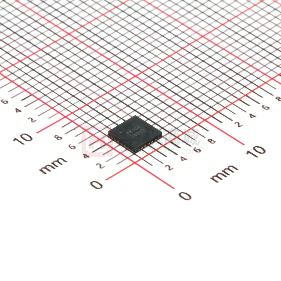
PAM8404
3W/CH FILTERLESS STEREO CLASS-D AUDIO AMPLIFIER
Description
Pin Assignments
The PAM8404 is a 3W high efficiency filterless Class-D audio
amplifier in 4mmX4mm and 2mmX2mm wafer chip scale (WCSP)
packages that requires few external components.
Features like 89% efficiency, -63dB PSRR, improved RF-rectification
immunity, and very small PCB area make the PAM8404 Class-D
amplifier ideal for cellular handset and PDA applications.
In cellular handsets, the earpiece, speaker phone, and melody ringer
can each be driven by the PAM8404. The PAM8404 allows
independent gain by summing signals from seperate sources, and
has as low as 43µV noise floor.
PAM8404 is available in QFN 4mmx4mm and WCSP 2mmx2mm
packages.
Features
3W Output at 10% THD with a 4Ω Load and 5V Supply
Supply Voltage from 2.5V to 5.5V
Efficiency Up to 89%
Superior Low Noise without Input
Few External Components to Save the Space and Cost
Short Circuit Protection
Thermal Shutdown
Space Saving Packages :
2mm X 2mmWCSP
4mm X 4mm Thin QFN
Pb-Free Packages
Applications
LCD Monitor / TV Projector
Notebook Computers
Portable Speakers
Portable DVD Players, Game Machines
Cellular Phones/Speaker Phones
PAM8404
Document number: DSxxxxx Rev. 1 - 1
1 of 18
www.diodes.com
November 2012
© Diodes Incorporated
�A Product Line of
Diodes Incorporated
PAM8404
Typical Applications Circuit
Pin Descriptions
Pin
Name
G1
OUTL+
PVDD
PGND
OUTLNC
SDL
SDR
AVDD
OUTROUTR+
G0
INR+
INRAGND
INLINL+
QFN4x4
1
2
313
412
5
610
7
8
9
11
14
15
16
17
18
19
20
Pin Number
WCSP2x2
B2
A3
A2
C4
A4
—
B4
B3
D2
D4
D3
C2
D1
C1
C3
B1
A1
PAM8404
Document number: DSxxxxx Rev. 1 - 1
Function
Gain Select (MSB)
Left Channel Positive Differential Output
Power Supply (Must be Same Voltage as AVDD)
Power Ground
Left Channel Negative Differential Output
Not Connected
Left Channel Shutdown Terminal (active low)
Right Channel Shutdown Terminal (active low)
Analog Supply (Must be Same Voltage as PVDD)
Right Channel Negative Differential Output
Right Channel Positive Differential Output
Gain Select (LSB)
Right Channel Positive Input
Right Channel Negative Input
Analog Ground
Left Channel Negative Input
Left Channel Positive Input
2 of 18
www.diodes.com
November 2012
© Diodes Incorporated
�A Product Line of
Diodes Incorporated
PAM8404
Functional Block Diagram
Absolute Maximum Ratings (@TA = +25°C, unless otherwise specified.)
These are stress ratings only and functional operation is not implied. Exposure to absolute maximum ratings for prolonged time periods may
affect device reliability. All voltages are with respect to ground.
Parameter
Supply Voltage
Input Voltage
Maximum Junction Temperature
Storage Temperature
Soldering Temperature
Rating
6.0
Unit
-0.3 to VDD +0.3
150
-65 to +150
250, 10sec
V
°C
Recommended Operating Conditions (@TA = +25°C, unless otherwise specified.)
Parameter
Supply Voltage Range
Operation Temperature Range
Junction Temperature Range
PAM8404
Document number: DSxxxxx Rev. 1 - 1
Rating
2.5 to 5.5
-40 to +85
-40 to +125
Unit
V
°C
°C
3 of 18
www.diodes.com
November 2012
© Diodes Incorporated
�A Product Line of
Diodes Incorporated
PAM8404
Thermal Information
Parameter
Thermal Resistance (Junction to Ambient)
Thermal Resistance (Junction to Case)
Package
WCSP2x2-16
QFN4x4-20
WCSP2x2-16
QFN4x4-20
Symbol
θJA
θJC
Max
64
31
—
13
Unit
°C/W
Electrical Characteristics (@TA = +25°C, AVDD = PVDD = 5V, GND = PGND = 0V, unless otherwise specified.)
QFN4X4-20
Symbol
VDD
Parameter
Test Conditions
THD+N = 1%, f = 1kHz, RL = 4Ω
Output Power
THD+N = 10%, f = 1kHz, RL = 8Ω
THD+N = 1%, f = 1kHz, RL = 8Ω
VDD = 5.0V, Po = 0.5W, RL = 8Ω
THD+N
Total Harmonic Distortion Plus
Noise
VDD = 3.6V, Po = 0.5W, RL = 8Ω
VDD = 5.0V, Po = 1W, RL = 4Ω
VDD = 3.6V, Po = 1W, RL = 4Ω
PSRR
CS
SNR
VN
Dyn
Power Supply Ripple Rejection
VDD = 5.0V, Inputs AC-Grounded with
CIN = 1.0μF
Crosstalk
VDD = 5V, Po = 0.5W, RL = 4Ω,
Gv = 23dB
Signal-to-Noise
VDD = 5V, VORMS = 1VGv = 23dB
Output Noise
VDD = 5V, Inputs AC-Grounded with
CIN = 1μF
BW 22Hz – 22kHz
Dynamic Range
η
Efficiency
IQ
Quiescent Current
ISD
RDS(ON)
Shutdown Current
Static Drain-to-Source On-State
Resistor
Typ
2.5
THD+N = 10%, f = 1kHz, RL = 4Ω
PO
Min
Supply Power
VDD = 5V, THD = 1%
RL = 8Ω, THD = 10%
RL = 4Ω, THD = 10%
VDD = 5.0V
VDD = 5.0V
3
VDD = 3.6V
1.5
VDD = 5.0V
2.35
VDD = 3.6V
1.2
VDD = 5.0V
1.7
VDD = 3.6V
0.9
VDD = 5.0V
1.4
VDD = 3.6V
0.7
f = 1kHz
f = 1kHz
VDD = 5.5V
IDS = 500mA,VGS = 5V
0.27
0.23
0.24
Units
5.5
V
W
W
W
W
%
%
f = 100kHz
f = 1kHz
-48
-63
dB
f = 1kHz
-93
dB
A-weighting
87
dB
A-weighting
43
No A-weighting
59
A-weighting
97
f = 1kHz
No load
VDD = 3.6V
0.15
Max
VSD = 0.3V
PMOS
NMOS
89
84
11
6
µV
dB
%
mA
很抱歉,暂时无法提供与“PAM8404KGR”相匹配的价格&库存,您可以联系我们找货
免费人工找货- 国内价格
- 1+3.26002
- 10+3.04002
- 50+2.71001
- 150+2.49000
- 300+2.33600
- 500+2.27000


 工商网监
湘ICP备2023018690号
工商网监
湘ICP备2023018690号

