PI3A4626
3.0V, SOTiny™ Single-Supply
0.4Ω SPST (NO) CMOS Analog Switch
Features
Description
• Low On-Resistance: 0.4Ω Max (+2.7V Supply)
PI3A4626 is a single-pole/single-throw (SPST) normally open
(NO) analog switch that operates from a single +1.5V to +3.6V
supply.
• 0.1Ω Max. On-Resistance Flatness at +25°C
• Fast Switching: 10ns Max.
The switch has 0.4Ω Max On-Resistance (RON), with 0.1Ω Max
RON flatness over the analog signal range when powered from a
+3.0V supply. Leakage currents are less than 2nA and fast switching times are less than 10ns.
• +1.5V to +3.6V Single-Supply Operation
• TTL/CMOS-Logic Compatible
• –25dB Off-Isolation at 100kHz
To minimize PC board area use, the device is available in a small
compact SOT23 package.
• 1nA Max. Off-Leakage at +25°C
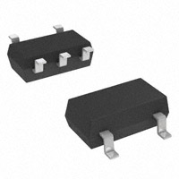
• Packaging (Pb-free & Green available):
– 5-pin Small Compact SOT23 (T)
Applications
• Cellular Phones
• Communications Circuits
• Battery-Operated Equipment
• DSL Modems
• Audio and Video Signal Routing
• PCMCIA Cards
Pin Description
Block Diagrams/Pin Configurations
SOT23
Name
Function
1
COM
Analog Switch, Common
2
NO
Analog Switch, Normally Open
3
GND
Ground
4
IN
Digital Control Input
5
VDD
Positive Supply Voltage
-
N.C.
No Internal Connection
Top Views
COM 1
5 VDD
NO 2
GND 3
Note:
1. NO and COM pins are identical and interchangeable. Any pin may
be considered as an input or an output; signals pass.
4 IN
SOT23
Truth Table
Input
Switch State
LOW
OFF
HIGH
ON
09-0003
1
PS8714D
10/26/09
�PI3A4626
3.0V, SOTiny™ Single-Supply
0.4Ω SPST (NO) CMOS Analog Switch
Absolute Maximum Ratings
Thermal Information
Voltages Referenced to GND
VDD....................................................................... –0.5V to +3.6V
Continuous Power Dissipation
SOT23 (derate 7.1mW/ºC above +70ºC)............................. 0.5W
VIN, VCOM, VNC, VNO (1). ...........................–0.5V to VDD +0.3V
or 30mA, whichever occurs first
Current (any terminal)...................................................... ±200mA
Peak Current, COM, NO, NC
(Pulsed at 1ms, 10% duty cycle)...................................... ±400mA
Storage Temperature ......................................... –65ºC to +150ºC
Lead Temperature (soldering, 10s).................................. +300ºC
Note:
1. Signals on NC, NO, COM, or IN exceeding VDD or GND are clamped by internal diodes. Limit forward diode current to 30mA.
Caution: Stresses beyond those listed under “Absolute Maximum Ratings” may cause permanent damage to the device. This is a
stress only rating and operation of the device at these or any other conditions beyond those indicated in the operational sections of
this specification is not implied.
Electrical Specifications - Single +3.3V Supply
(VDD = +3.3V ± 10%, GND = 0V, VIH = 1.4V, VIL = 0.5V)
Description
Parameters
Test Conditions
Package
Temp.(°C)
Min.(1)
Full
0
Typ.(2)
Max.(1)
Units
VDD
V
Analog Switch
Analog Signal Range(3)
VANALOG
25
0.4
Full
0.5
25
0.05
Full
0.06
25
0.1
RFLAT(ON)
VDD =2.7V
ICOM = 100mA,
VNO or VNC =0.8V,
2.0V
Full
0.1
ICOM(OFF) or
INC(OFF)
VDD =3.3V,
VCOM = 0V,VNO or
VNC = +2.0V
25
–1
1
Full
–20
10
25
–2
2
ICOM(ON)
VDD =3.3V,
VCOM = +2.0V,
VNO or
VNC = + 2.0V
Full
–20
20
On Resistance
RON
On-Resistance Match
Between Channels(4)
∆RON
On-Resistance
Flatness(5)
NO or NC Off Leakage
Current(6)
COM On Leakage Current(6)
09-0003
VDD = 2.7V,
ICOM = 100mA,
VNO or VNC =
+1.5V
SOT23
2
PS8714D
Ω
nA
10/26/09
�PI3A4626
3.0V, SOTiny™ Single-Supply
0.4Ω SPST (NO) CMOS Analog Switch
Electrical Specifications - Single +3.3V Supply (continued)
(VDD = + 3.3V ± 10%, GND = 0V, VIH = 1.4V, VIL = 0.5V)
Parameters
Test Conditions
Temp (ºC) Min.(1) Typ.(2) Max.(1) Units
Input High Voltage
VIH
Guaranteed logic High Level
Full
Input Low Voltage
VIL
Guaranteed logic Low Level
Input Current with Voltage
IINH
High
VIN = 1.4V, all others = 0.5V
–1
1
Input Current with Voltage
IINL
Low
VIN = 0.5V, all other = 1.4V
–1
1
Description
Logic Input
1.4
0.5
V
µA
Dynamic
Turn-On Time
Turn-Off Time
tON
VDD = 3.3V, VNO or
VNC = 2.0V, Figure 1
tOFF
Charge Injection(3)
Q
Off Isolation(7)
CL = 1nF, VGEN = 0V,
RGEN = 0Ω, Figure 2
OIRR
RL = 50Ω, f = 100kHz, Figure 3
NC or NO Capacitance
C(OFF)
COM Off Capacitance
CCOM(OFF)
COM On Capacitance
CCOM(ON)
25
10
Full
10
25
10
Full
10
25
ns
50
pC
-25
dB
130
f = 1 MHz, Figure 4
pF
130
f = 1 MHz, Figure 4
270
Supply
Power Supply Range
VDD
Positve Supply Current
ICC
Full
VDD = 3.6V, VIN = 0V or VDD
1.5
3.6
V
100
nA
Notes:
1. The algebraic convention, where most negative value is a minimum and most positive is a maximum, is used in this data sheet.
2. Typical values are for DESIGN AID ONLY, not guaranteed or subject to production testing.
3. Guaranteed by design.
4. ΔRON = RON Max. - RON Min.
5. Flatness is defined as the difference between the maximum and minimum value of On-Resistance measured.
6. Leakage parameters are 100% tested at maximum rated hot temperature and guaranteed by correlation at +25ºC.
7. Off Isolation = 20log10 [ VCOM / (VNO or VNC) ]. See Figure 3.
09-0003
3
PS8714D
10/26/09
�PI3A4626
3.0V, SOTiny™ Single-Supply
0.4Ω SPST (NO) CMOS Analog Switch
Electrical Specifications - Single +2.5V Supply
(VDD = +2.5V ± 10%, GND = 0V, VIH = 1.4V, VIL = 0.5V)
Description
Parameters Test Conditions
Temp.(°C)
Min.(1)
Typ.(2)
Max.(1)
Units
VDD
V
Analog Switch
Analog Signal Range(3)
VANALOG
On-Resistance
RON
On-Resistance Match
Between Channels(4)
∆RON
On-Resistance Flatness(5)
RFLAT(ON)
0
VDD = 2.5V, ICOM = –8mA,
VNO or VNC = 1.8V
VDD = 2.5V, ICOM = –8mA,
VNO or VNC = 0.8V, 1.8V
25
0.4
Full
0.4
25
0.05
Full
0.06
25
0.1
Full
0.1
25
10
Full
15
25
10
Full
10
Ω
Dynamic
Turn-On Time
tON
VDD = 2.5V,
VNO or VNC = 1.8V, Figure 1
Turn-Off Time
tOFF
Charge Injection(3)
Q
CL = 1nF, VGEN = 0V,
RGEN = 0V, Figure 2
25
Input HIGH Voltage
VIH
Guaranteed logic high level
Full
Input LOW Voltage
VIL
Guaranteed logic Low level
Full
Input HIGH Current
IINH
VIN = 1.4V, all others = 0.5V
Full
–1
1
Input HIGH Current
IINL
VIN = 0.5V, all others = 1.4V
Full
–1
1
42
ns
pC
Logic Input
1.4
0.5
V
µA
Notes:
1. The algebraic convention, where most negative value is a minimum and most positive is a maximum, is used in this data sheet.
2. Typical values are for DESIGN AID ONLY, not guaranteed or subject to production testing.
3. Guaranteed by design.
4. ΔRON = RON max. - RON min.
5. Flatness is defined as the difference between the maximum and minimum value of On-Resistance measured.
09-0003
4
PS8714D
10/26/09
�PI3A4626
3.0V, SOTiny™ Single-Supply
0.4Ω SPST (NO) CMOS Analog Switch
Electrical Specifications - Single +1.8V Supply
(VDD = +1.8V ± 10%, GND = 0V, VIH = 1.4V, VIL = 0.5V)
Description
Parameters
Test Conditions
Temp.(°C)
Min.(1)
Typ.(2) Max.(1)
Units
Analog Switch
Analog Signal Range(3)
VANALOG
On-Resistance
RON
VDD = 1.8V, ICOM = –4mA,
VNO or VNC = 1.5V
25
0.4
Full
0.8
On-Resistance Match
Between Channels(4)
∆RON
VDD = 1.8V, ICOM = –4mA,
VNO or VNC = 0.8V,1.5V
25
0.05
Full
0.06
On-Resistance Flatness(5)
RFLAT(ON)
25
0.4
Full
0.6
25
15
Full
15
25
10
Full
15
0
VDD
V
Ω
Dynamic
Turn-On Time
Turn-Off Time
tON
tOFF
VDD = 1.8V, VNO or VNC =
1.5V, Figure 1
Q
CL = 1nF, VGEN = 0V,
RGEN = 0V, Figure 2
25
Input HIGH Voltage
VIH
Guaranteed logic high level
Full
Input LOW Voltage
VIL
Guaranteed logic Low level
Full
Input HIGH Current
IINH
VIN = 1.4V, all others = 0.5V
Full
–1
1
Input HIGH Current
IINL
VIN = 0.5V, all others = 1.4V
Full
–1
1
Charge Injection(3)
29
ns
pC
Logic Input
1.4
0.5
V
µA
Notes:
1. The algebraic convention, where most negative value is a minimum and most positive is a maximum, is used in this data sheet.
2. Typical values are for DESIGN AID ONLY, not guaranteed or subject to production testing.
3. Guaranteed by design.
4. ΔRON = RON max. - RON min.
5. Flatness is defined as the difference between the maximum and minimum value of On-Resistance measured.
09-0003
5
PS8714D
10/26/09
�PI3A4626
3.0V, SOTiny™ Single-Supply
0.4Ω SPST (NO) CMOS Analog Switch
Test Circuits/Timing Diagrams
VDD
Switch
+3V*
Input
VDD
NO
COM
RL
50ohm
IN
Logic
Input
VOUT
CL
35pF
GND
Logic VINH
Input
VINL
Switch
Output
0V
tr