UM Series Crystal Clock Oscillator (XO)
2.0 x 1.6 x 0.60mm
UM
1.8V Clipped Sinewave Low Jitter XO
Package:
2.0 x 1.6mm Ceramic SMD
Recommended Land Pattern:
Product Features
• Very low Phase Jitter-2ps RMS (10kHz-5MHz)
• Low output current - 2mA Max
• Low power standby mode - 10mA Max
• Low Output Harmonic level
CREATED USING CADSTD LITE FREEWARE FROM WWW.CADSTD.COM. NON-COMMERCIAL USE ONLY.
• RoHS Compliant
Pin Functions:
Product Description
This is an enhanced 1.8V crystal clock clipped
sine oscillator with superb phase jitter, low
output harmonics and operating current for WiFi
/Bluetooth wireless module and smart phone
applications
Pin
Function
1
OE Function
2
Ground
3
Clock Output
4
V DD
Applications
• WiFi/Bluetooth wireless module
• Smart phone
*Extended high frequency power decoupling is recommended (see test circuit for minimum
recommendation). To ensure optimal performance, do not route RF traces beneath the
CREATED USING
CADSTD LITE FREEWARE FROM WWW.CADSTD.COM. NON-COMMERCIAL USE ONLY.
package.
Part Ordering Information:
UM XXX YYYY
YYYY = Specification�Code
XXX = Frequency�Code
Product�Family
SaRonix-eCera™ is a Pericom® Semiconductor company
11-0021
•
US: +1-408-435-0800 TW: +886-3-4518888 • www.saronix-ecera.com
All specifications are subject to change without notice.
UM 1.8 REV2011_MAY10_10.5
1
�1.8V Clipped Sinewave Low Jitter XO
UM
UM Series Crystal Clock Oscillator (XO)
2.0 x 1.6 x 0.60mm
Electrical Performance
Parameter
Min.
Output Frequency
Typ.
1
Supply Voltage
1.62
1.8
Supply Current, Output Enabled
Supply Current, Standby Mode
Output Voltage
Units
50
MHz
1.98
V
2
mA
10
mA
±20 to ±50
ppm
-20
+70
°C
-40
+85
Frequency Stability
Operating Temperature Range
Max.
0.4
0.9
Output Load
See Note 1 below
Commercial (standard)
Industrial (standard)
Vp-p
10/10
Duty Cycle
Notes
pF/kW
45
Jitter, Phase
55
%
2
ps RMS
Measured 50% of V DD
1-s, 10kHz to 5 MHz frequency band
Notes:
1. Stability includes all combinations of operating temperature, load changes, rated input (supply) voltage changes, initial calibration tolerance (25°C),
aging (5 year at 40°C average effective ambient temperature), shock and vibration.
2. For specifications othere than those listed, please contact sales.
Output Enable / Disable Function
Parameter
Min.
Input Voltage (pin 1), Output Enable
Typ.
Max.
0.7 V DD
Units
Notes
V
Input Voltage (pin 1), Output Disable (low power standby)
0.3 V DD
V
Output Disable Delay
100
ns
Output Enable Delay
10
ms
Output is Hi-Z
Absolute Maximum Ratings
Parameter
Storage Temperature
For the latest product information visit:
For test circuit go to:
Min.
Typ.
-55
Max.
Units
+125
°C
Notes
http://www.pericom.com/products/timing/oscillators/UM_1.8V/
http://www.pericom.com/pdf/sre/tc_clipsine2.pdf
For soldering reflow profile and reliability test ratings go to: http://www.pericom.com/pdf/sre/reflow2.pdf
For tape and reel information go to: http://www.pericom.com/pdf/sre/tr_2016_xo.pdf
SaRonix-eCera™ is a Pericom® Semiconductor company
11-0021
•
US: +1-408-435-0800 TW: +886-3-4518888 • www.saronix-ecera.com
All specifications are subject to change without notice.
UM 1.8 REV2011_MAY10_10.5
2
�
很抱歉,暂时无法提供与“UM2600001”相匹配的价格&库存,您可以联系我们找货
免费人工找货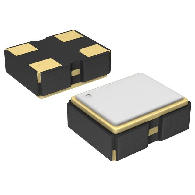


 工商网监
湘ICP备2023018690号
工商网监
湘ICP备2023018690号
