User's Guide
SBAU203 – July 2013
ADS1x20EVM
ADS1x20EVM
This user's guide describes the characteristics, operation, and use of the ADS1x20EVM. These evaluation
modules are an evaluation system for the ADS1220, a 24-bit, low-power, multichannel, delta-sigma (ΔΣ),
analog-to-digital converter (ADC) and the ADS1120, which is the 16-bit version of the ADS1220. The EVM
allows evaluation of all aspects of the ADS1x20 devices.
This document includes an EVM Quick Start, hardware and software details, bill of materials, and
schematic. Table 1 lists the related documents available through the Texas Instruments web site at
www.ti.com.
Table 1. EVM-Compatible Device Data Sheets
Device
Literature Number
Device
Literature Number
ADS1120
SBAS535
MSP430F5528
SLAS590
ADS1220
SBAS501
TPS3838L30
SLVS292
SN74LVC2G157
SCES207
SN74LVC125A
SCAS290
TPS76333
SLVS181
—
—
MSP430, ADCPro are trademarks of Texas Instruments.
SPI is a trademark of Motorola.
I2C is a trademark of NXP Semiconductors.
Omega is a registered trademark of Omega Engineering Limited.
Samtec is a trademark of Samtec, Inc.
Vishay is a registered trademark of Vishay Intertechnology, Inc.
All other trademarks are the property of their respective owners.
SBAU203 – July 2013
Submit Documentation Feedback
ADS1x20EVM
Copyright © 2013, Texas Instruments Incorporated
1
�www.ti.com
1
2
3
4
5
6
Contents
EVM Overview ............................................................................................................... 3
Quick Start ................................................................................................................... 4
Quick Reference ............................................................................................................ 5
Using the ADS1220EVM ADCPro Plug-in ............................................................................... 6
ADS1220EVM Hardware Details ........................................................................................ 10
Schematic and Bill of Materials .......................................................................................... 16
List of Figures
1
ADS1x20EVM Default Jumper Locations ................................................................................ 4
2
I/O Config .................................................................................................................... 7
3
Current and Ref ............................................................................................................. 8
List of Tables
2
1
EVM-Compatible Device Data Sheets ................................................................................... 1
2
Default Jumper and Switch Configuration ............................................................................... 4
3
Critical Connections
4
Jumper and Switch Descriptions ........................................................................................ 10
5
J4: Primary Analog Interface Pinout .................................................................................... 11
6
J1 and J6: Bridge Sensor Connectors .................................................................................. 11
7
J2: RTD Terminal Block Connector ..................................................................................... 12
........................................................................................................
5
8
J5: Auxiliary Connector ................................................................................................... 13
9
JTAG Interface Connections ............................................................................................. 14
10
JAC: External Interface Connector ...................................................................................... 15
11
JDB: External Interface Connector ...................................................................................... 15
12
ADS1x20EVM Bill of Materials
..........................................................................................
ADS1x20EVM
16
SBAU203 – July 2013
Submit Documentation Feedback
Copyright © 2013, Texas Instruments Incorporated
�EVM Overview
www.ti.com
1
EVM Overview
The ADS1x20EVM is an evaluation module that includes an MSP430™ microcontroller and software. The
ADS1x20EVM is useful for prototyping designs and firmware as well as for evaluation.
1.1
Features
ADS1x20EVM Features:
• Contains all support circuitry needed for the ADS1120 and ADS1220
• Voltage reference options: internal or external
• Clock options: internal or external
• MSP430 microcontroller with JTAG interface
• Compatible with the TI LaunchPad
The ADS1x20EVM includes an interface for serial communication that can be used with ADCPro™ to
quickly evaluate the device.
This manual covers the operation of the ADS1x20EVM. Throughout this document, the abbreviation EVM
and the term evaluation module are synonymous with the ADS1120EVM and ADS1220EVM. For clarity of
reading, the remainder of this manual refers only to the ADS1220EVM, but operation of the EVM for the
ADS1120 is identical, unless otherwise noted.
SBAU203 – July 2013
Submit Documentation Feedback
ADS1x20EVM
Copyright © 2013, Texas Instruments Incorporated
3
�Quick Start
2
www.ti.com
Quick Start
This section provides a Quick Start guide to quickly begin evaluating the ADS1220EVM with ADCPro.
2.1
Default Jumper and Switch Configuration
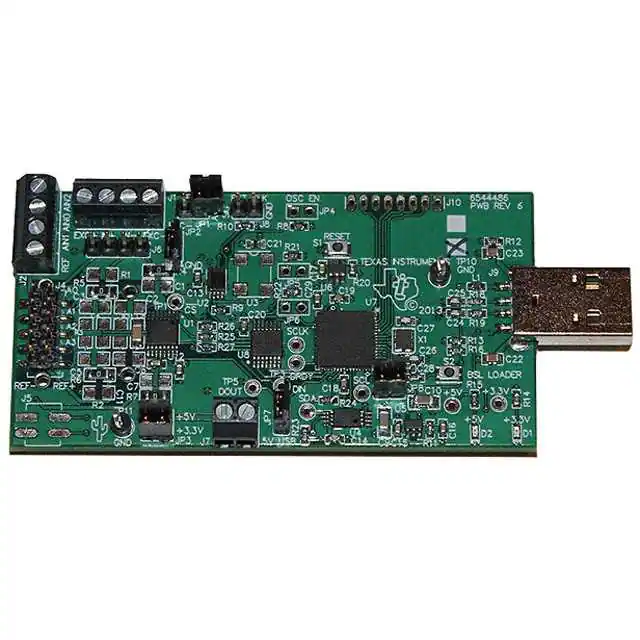
Figure 1 shows the jumpers found on the EVM and the respective factory default conditions for each.
Figure 1. ADS1x20EVM Default Jumper Locations
Table 2 lists the primary jumpers and the factory default conditions.
Table 2. Default Jumper and Switch Configuration
2.2
Jumper
Default Position
JP1
Open
Description
EXC+ connected to AVDD
JP2
Open
EXC- connected to AGND
JP3
Short pins 2-4
JP7
Short
USB power connected to +5 V
JP8
Short
U5 output connected to +3.3 V
AVDD supply connection to +5 V or +3.3 V (default to +3.3 V)
ADS1220EVM Operation
To prepare to evaluate the ADS1220 with the ADS1220EVM, complete the following steps:
1. Verify the jumpers on the ADS1220EVM are as shown in Figure 1 (note that these settings are the
factory-configured settings for the EVM).
2. Using ADCPro HW/SW Installation Manual, install the ADCPro and ADS1220EVM plug-in software.
Plug-in software installs the necessary driver for USB communication.
3. Plug the ADS1220EVM into an available USB port. The EVM is configured to power from the USB
port.
4
ADS1x20EVM
SBAU203 – July 2013
Submit Documentation Feedback
Copyright © 2013, Texas Instruments Incorporated
�Quick Reference
www.ti.com
3
Quick Reference
Table 3 provides a quick summary of the key connections necessary for EVM operation. This information
is helpful when using an external processor, or for monitoring EVM operation.
Table 3. Critical Connections
Function
SPI
Power
Analog inputs
Pin Name
Description
CS
JAC.3 (TP1)
CS
Chip select
SCLK
JDB.16 (TP2)
SCLK
Serial clock
DIN
JAC.15 (TP3)
DIN
DOUT/DRDY
JDB.18 (TP5)
DOUT
Data out
DRDY
JAC.11 (TP4)
DRDY
Data ready
+3.3 V
JAC.1 (TP9)
+3.3V
Digital or analog supply
+5 V
JAC.2, J7 (TP8)
+5V
Channel 1
J1.4, J2.2, J4.2,
J6.4
AIN0/REFP1
Channel 2
J1.3, J2.3, J3.2,
J4.4, J6.3
AIN1
Analog input
Channel 3
J1.2, J2.1, J3.1,
J4.6, J6.2
AIN2
Analog input
Channel 4
J1.1, J4.8, J6.1
AIN3/REFN1
External reference
3.1
Header (Pin)
Data in
Analog supply
Analog or reference input
Analog or reference input
J2.4, J4.10
REFP0
Reference input (+)
J4.9
REFN0
Reference input (–)
Analog Inputs
The analog inputs for the ADS1220EVM are connected to J1, J2, J3, J4, and J6. Channels 1 to 4 and the
external reference, connect to header J4.
3.2
Digital Control
The digital control signals can be applied directly to connectors JAC and JDB. The connector footprints
are on the bottom side of the board and the connectors are not installed.
3.3
Power Supply
The ADS1220EVM requires power rails as follows:
• +5-V analog supply: supplied by USB or from an external source connected to J7.
• +3.3-V digital or analog supply: can be supplied from the +5-V supply.
3.4
Voltage Reference
The ADS1220EVM has three options for the reference voltage: an internal reference and two possible
external reference inputs (REF0 and REF1). The ADS1220 internal reference is selected at power up.
Two external reference connections are available as follows:
• REF0 dedicated reference input connected to J2.4 and J4.9-10, and
• REF1 shared with analog inputs connected to J1.1, J1.4, J2.2, J4.2, J4.8, J6.1, and J6.4.
SBAU203 – July 2013
Submit Documentation Feedback
ADS1x20EVM
Copyright © 2013, Texas Instruments Incorporated
5
�Using the ADS1220EVM ADCPro Plug-in
4
www.ti.com
Using the ADS1220EVM ADCPro Plug-in
The ADS1220EVM plug-in for ADCPro provides complete control over all settings of the ADS1220. The
plug-in consists of a tabbed interface (see Figure 2), with different functions available on different tabs.
The tabs are:
• I/O Config
• Current & Ref
• About
The user can adjust the ADS1220EVM settings when not acquiring data. During acquisition, all controls
are disabled and settings may not be changed. When a setting is changed on the ADS1220EVM plug-in,
the setting immediately updates on the board. Settings on the ADS1220EVM correspond to settings
described in the ADS1220 product data sheet.
4.1
Top-Level Controls
The ADS1220EVM settings can be adjusted when not acquiring data. During acquisition, all controls are
disabled and settings may not be changed.
The effective data rate of the ADS1220 depends upon the frequency of the clock used. The default
operating mode is the internal clock oscillator of the ADS1220, which is 4.096 MHz. The Data Rate
indicator in the upper right corner of the plug-in interface (see Figure 2) is always visible and updates
whenever a setting changes that affects the data rate. The indicated values are representative of the
internal clock frequency of the ADS1220 and the operating clock mode (Normal, Duty-Cycle, or Turbo).
The default operating mode is Normal. The Data Rate is adjusted by making the desired selection from
the drop-down menu.
The Gain indicator in the upper left corner of the plug-in interface (see Figure 2) is always visible and
updates whenever a setting changes that affects the gain. The indicated values are representative of the
state of the PGA Bypass. If PGA Bypass is selected on the I/O Config tab (as shown in Figure 2), only
gains of 1, 2, and 4 are bypassed from the PGA. All other gain settings require the PGA to be enabled.
When higher gains are selected, the PGA is enabled regardless of the PGA Bypass state. To limit
confusion regarding the state of the PGA, the only possible selections for PGA Bypass is 1, 2, or 4 from
the drop-down menu.
The only way to view output data results is by operating the ADS1220 in continuous conversion mode.
This mode is identified by the Cont Conv button indicator (as shown in Figure 2) on the bottom left of the
ADS1220EVM plug-in. The button is lit green when in continuous conversion mode, otherwise the
ADS1220 is in single conversion mode in a power-down state. No data can be collected while not in Cont
Conv and are only useful for monitoring supply currents to determine power consumption of the ADS1220
while in power-down.
6
ADS1x20EVM
SBAU203 – July 2013
Submit Documentation Feedback
Copyright © 2013, Texas Instruments Incorporated
�Using the ADS1220EVM ADCPro Plug-in
www.ti.com
4.2
I/O Config Tab
The ADS1220 can acquire data from only one channel at a time. The I/O Config tab (as shown in
Figure 2) provides control of the MUX selection. MUX selections correspond to settings described in the
ADS1220 product data sheet. The remaining control settings discussed in this document also correspond
to settings described in the product data sheet.
Figure 2. I/O Config
Operating Mode controls the speed of the modulator clock. Depending on the Operating Mode selected
from the drop-down menu, the Data Rate changes appropriately. Normal is the normal operating mode of
the ADS1220, Turbo doubles the Data Rate from Normal, and Duty-Cycle mode reduces the Data Rate
from Normal by four.
FIR Filter settings enable changes to be made to the output response of the digital filter. The default
condition is to have No 50/60 Hz Rejection. Other options from the drop-down menu allow for
Simultaneous 50/60 Hz Rejection, 50 Hz Rejection Only, or 60 Hz Rejection Only.
Four other button options appear on the I/O Config tab. The first button controls the PGA Bypass. When
the PGA Bypass button is active (indicated when lit green), the Gain choice is limited to 1, 2, or 4. The
benefit of using PGA Bypass is removing the common-mode input restriction of the PGA so the full
analog supply range for single-ended measurements can be used. This benefit, however, comes at the
cost of lowered input impedance for the ADS1220.
The Burnout Current Sources button controls the 10-µA burnout current sources. When this button is lit
green, the burnout current is routed through the selected MUX channel and detects any breaks or shorts
to a connected sensor.
SBAU203 – July 2013
Submit Documentation Feedback
ADS1x20EVM
Copyright © 2013, Texas Instruments Incorporated
7
�Using the ADS1220EVM ADCPro Plug-in
www.ti.com
When the Internal Temperature Sensor button is activated and lit green, the output result from the
ADS1220 is the response of the internal temperature sensor of the ADS1220. The temperature sensor is a
precision device and can monitor the internal temperature of the ADS1220. The temperature sensor can
also be used for making cold-junction temperature measurements when using thermocouples.
When lit green, the Low-Side Power Switch button allows for direct connection of the AIN3 input to
AVSS while the ADS1220 is converting. This connection is useful when making bridge-type
measurements and trying to conserve power. Power conservation is due to bridge excitation only taking
place while the ADS1220 is converting. Demonstrating the usefulness of this option using the
ADS1220EVM plug-in is difficult because the ADS1220 is always collecting data in the continuous
conversion mode of operation. However, power savings can be calculated by comparing the total power
used while converting, as compared to the total power of the power-down mode.
4.3
Current & Ref Tab
The Current & Ref tab allows various reference options to be selected along with the control and routing
of IDAC currents, as shown in Figure 3.
Figure 3. Current and Ref
Reference Select selects the reference for the ADS1220. The drop-down menu lists four options. The
Internal Reference selection uses the ADS1220-derived, 2.048-V reference. The three remaining options
use the voltage connected to the REFP0, REFP1, or the analog supply voltage (AVDD). When using a
test plug-in with ADCPro, the output results displayed as volts are determined according to the VREF
indicator voltage. The value of VREF defaults to 2.048 V, which is the internal voltage reference of the
ADS1220. When using an external reference, change the VREF indicator to the appropriate reference
voltage value. This adjustment ensures that the results displayed in the test plug-in of ADCPro are
changed to the correct value.
8
ADS1x20EVM
SBAU203 – July 2013
Submit Documentation Feedback
Copyright © 2013, Texas Instruments Incorporated
�Using the ADS1220EVM ADCPro Plug-in
www.ti.com
The IDAC Magnitude drop-down menu allows the choice of current settings for the constant-current
output digital-to-analog converters (DACs) of the ADS1220. Two current output DACs are available and
can be routed independent of one another through the IDAC 1 Routing and IDAC 2 Routing controls.
However, the IDAC Magnitude is the same for both current sources and the current output is not
independently controlled. No current sources from the IDACs if the IDAC Magnitude is Off. This condition
is true even if the IDAC routing controls have the IDACs routed to a specified output. The seven output
current magnitude options are 10uA, 50uA, 100uA, 250uA, 500uA, 1000uA, and 1500uA. If both IDACs
are routed to the same output, the IDAC current available is twice the indicated IDAC Magnitude.
The IDAC current sources can be routed independently or to the same output. The control for the IDAC 1
Routing and IDAC 2 Routing have the same drop-down menu options. If the IDAC routing is Off, then
the IDAC being controlled is disabled and no current is sourced. This condition is true even if the IDAC
Magnitude indicates an available current. The IDAC current can be routed out through any of the analog
or reference input channels.
4.4
About Tab
The About tab provides information on the EVM hardware and software versions.
Plug-in Version is the software version of the ADCPro plug-in.
Firmware Version is the firmware version loaded and running on the processor.
SBAU203 – July 2013
Submit Documentation Feedback
ADS1x20EVM
Copyright © 2013, Texas Instruments Incorporated
9
�ADS1220EVM Hardware Details
5
www.ti.com
ADS1220EVM Hardware Details
The ADS1220EVM is designed to easily interface with other control platforms. Dual-row socket options
(JAC and JDB) are available on the bottom-side of the EVM, which allows for the controller connection.
The pin configuration of the connectors is designed to be compatible with LaunchPad. The connector
footprint conforms to Samtec™ connector SSW-110-22-F-D-VS-K, which is a dual-row, 20-pin, surfacemount socket with a 0.1-inch pitch spacing.
Another method of controlling the ADS1220 is by connecting control signals to the test points for digital
communication to the ADS1220.
If using another controller other than the on-board MSP430, the control signals for this device must
become inoperative. To deactivate the on-board processor, short the JP5 pins, which places the output of
buffer U8 into a 3-state condition. Jumper JP5 is not installed by default. A wire can be soldered to the
terminals of JP5, or a standard 0.1-inch pitch header with shorting block can be installed.
5.1
Jumpers and Switches
Jumpers and switches function as shown in Table 4.
Table 4. Jumper and Switch Descriptions
Jumper or
Switch
5.2
Functions
Descriptions
JP1
EXC+ source
Short: Connect AIN0 (EXC+ of J1.4 and J6.4) to AVDD
Open: AIN0 is not connected to AVDD (default)
JP2
EXC– source
Short: Connect AIN3 (EXC– of J1.1 and J6.1) to AGND
Open: AIN3 is not connected to AGND (default)
JP3
Analog supply source
Short 1 to 2 (top): AVDD is connected to +5 V
Short 3 to 4 (bottom): AVDD is connected to +3.3 V (default)
JP4
Clock source
Short: External oscillator is used as the clock source (requires installation)
Open: On-board or external (J8) clock source (default)
JP5
Digital control source
Short: External controller
Open: On-board controller
JP6
External clock source
Short: Controller clock (not currently available)
Open: Connected J8 clock source (default)
JP7
+5-V source
Short: Powered from the USB (default)
Open: +5 V supplied at J7 (also available at the JAC pin 2 and +5-V test
point)
JP8
+3.3-V source
Short: Regulated LDO on-board supply (default)
Open: Supplied externally at JAC or to +3.3-V test point
S1
Controller reset
Normally open SPST push-button resets controller on button press
S2
Controller BSL
Normally open SPST push-button enters controller bootstrap loader (BSL)
mode with button press while +3.3-V power is applied
Analog Headers, Terminal Blocks, and J3
For maximum flexibility, the ADS1220EVM is designed for easy interfacing to multiple analog sources.
These connectors provide access to the analog input pins of the ADS1220.
The EVM is designed to accept multiple sensor types. The sensor types can range from thermocouples,
resistance temperature detectors (RTDs), load cells, pressure, and so forth. The analog inputs can be
filtered by installing passive components in the optional filter circuitry. By default, the series input resistors
are populated with 0-Ω resistors and the capacitors are not installed. No circuitry is provided to buffer
these signals before connecting to the converter.
10
ADS1x20EVM
SBAU203 – July 2013
Submit Documentation Feedback
Copyright © 2013, Texas Instruments Incorporated
�ADS1220EVM Hardware Details
www.ti.com
5.2.1
Primary Analog Interface, J4
All available analog pins of the ADS1220 connect to header J4. J4 can be used to connect analog signals
from off-board sensors or sources to the ADS1220. Table 5 provides J4 pin descriptions. J4 is a standard
10-pin, dual-row header, with 0.1-inch pin spacing.
Table 5. J4: Primary Analog Interface Pinout
Description
Signal
Pin Number
Analog dedicated reference input, negative
REFN0
J4.9
Analog dedicated reference input, positive
REFP0
J4.10
AGND
J4.1 (1)
AGND
J4.3
AGND
J4.5
Analog ground
AGND
J4.7
Analog input channel 1
AIN0/REFP1
J4.2
Analog input channel 2
AIN1
J4.4
Analog input channel 3
AIN2
J4.6
Analog input channel 4
AIN3/REFN1
J4.8
(1)
5.2.2
Pin 1 is at the top left-hand corner, located opposite of the reference designator.
Bridge Sensor Connectors, J1 and J6
Connectors J1 and J6 are designed to be used with bridge sensor applications. J1 is a four-position screw
terminal block that can accept wire sizes AWG 28-16. J6 is a standard single-row, 4-pin header with 0.1inch pin spacing. Both connectors allow for excitation to be connected to the outer pins while the
differential signals from the sensor connect to the inner pins. Table 6 lists pin descriptions.
Bridge excitation is provided from the analog supply as needed. JP1 connects EXC+ directly to AVDD.
JP2 connects EXC– directly to AGND. To conserve power, EXC– can also be connected to AGND
through the low-side switch of the ADS1220.
Table 6. J1 and J6: Bridge Sensor Connectors
Description
Signal
Pin Number
Analog input, negative (IN–)
AIN2
J1.2 or J6.2
AIN1
J1.3 or J6.3
Bridge excitation, negative (EXC–)
Negative reference input for ratiometric measurement (REFN1)
AIN3/REFN1
J1.1 (2) or J6.1 (2)
Bridge excitation, positive (EXC+) (3)
Positive reference input for ratiometric measurement (REFP1)
AIN0/REFP1
J1.4 or J6.4
Analog input, positive (IN+)
(1)
(1)
(2)
(3)
EXC– can be connected to AGND through JP2, or through the low-side switch of AIN3/REFN1 of the ADS1220.
Pin 1 is at the top right-hand corner, located next to the reference designator.
EXC+ can be connected to AVDD through JP1.
SBAU203 – July 2013
Submit Documentation Feedback
ADS1x20EVM
Copyright © 2013, Texas Instruments Incorporated
11
�ADS1220EVM Hardware Details
5.2.3
www.ti.com
RTD Terminal Block J2
J2 is a four-position screw terminal block that can accept wire sizes AWG 28-16. The main purpose for J2
is to provide a connection for measuring a resistance temperature device (RTD). A two-, three-, or fourwire RTD can be connected to J2. Measurement channels are AIN0 and AIN1. Current excitation is
directly possible from AIN0, AIN1, and AIN2. For three-wire RTDs, any combination of two excitation
sources can be used.
One problem with using a three-wire RTD is in regards to driving current through analog input filtering.
This problem can be avoided by installing resistor R30, which allows AIN3 to be used as a second current
source. Placing a 0-Ω resistor at R30 creates a direct connection between AIN3 and J2.3 (AIN1). Table 7
lists pin descriptions.
RTD measurement is best as a ratiometric measurement. Excitation current establishes a reference
voltage at the dedicated reference REP0/REFN0. 'Establishing the reference voltage requires that a bias
resistor be installed at R3. R3 should be a precision, low-drift resistor. The value chosen depends on the
RTD value and excitation current, as well as maintaining IDAC voltage compliance for the ADS1220. For a
complete current path, one side of R3 (REFN0 side) must connect to AGND. The easiest way to
accomplish this connection is to place a shorting jumper from J4.9 to J4.7.
Table 7. J2: RTD Terminal Block Connector
Description
Signal
Pin Number
Analog input, negative (IN–)
AIN1
J2.3 (1)
AIN0
J2.2
REFP0
J2.4
AIN2
J2.1 (4)
Analog input, positive (IN+)
Reference bias resistor connection
RTD current excitation
(1)
(2)
(3)
(4)
5.2.4
(2)
(3)
When using a three-wire RTD, AIN3 can be used as a current source by installing a 0-Ω resistor at R30.
Bias resistor R3 must be installed. To complete the current path, REFN0 must also be connected to ground.
Direct connection to three- and four-wire RTDs. A two-wire RTD requires a jumper between J2.1 and J2.2 as well as between
J2.3 and J2.4. Three-wire RTDs require an additional excitation current.
Pin 1 is at the top left-hand corner of the EVM, located opposite from the reference designator.
Thermocouple Connector, J3
Provision for a miniature thermocouple connector is provided on the EVM. The socket connector footprint
accommodates the Omega® PCC-SMP-style connector at J3. The J3 connector should be installed on the
bottom-side of the EVM. The J3 terminals connect to AIN1 and AIN2 of the ADS1220. Biasing resistors R1
and R2 can be installed to place the thermocouple into the correct common-mode input range of the
ADS1220.
A cold-junction area is provided for compensation (CJC) and the ADS1220 temperature sensor can be
used to measure the temperature of the cold junction. Provision for a RTD chip temperature-sensing
device is located at R31. An example of what can be used at R31 is the Vishay® Beyschlag
PTS120601B100RP100. When using a RTD at R31, excitation current is provided from AIN3. For a
complete current path, AIN3 must connect to R31. This connection can be accomplished by placing a
jumper wire at J4.2 to J4.8 of connector J4. Similar jumper options are also available at connectors J1 and
J6.
5.2.5
Analog Input Filtering Options
The analog input connectors directly connect to the ADS1220 inputs using 0-Ω resistors by default. Filters,
such as antialiasing or electromagnetic interference and radio frequency interference (EMI/RFI), can be
installed using the resistor and capacitor pads available at the analog side of the ADS1220. These pads
are found on both the top- and bottom-side of the EVM. Device pads are available to create filter
combinations for both differential and common-mode filters for many different input configurations. Filtering
combinations are also included for filtering the external reference inputs.
12
ADS1x20EVM
SBAU203 – July 2013
Submit Documentation Feedback
Copyright © 2013, Texas Instruments Incorporated
�ADS1220EVM Hardware Details
www.ti.com
5.3
Clock Source Options
The ADS1220 clock can come from one of several sources: the internal oscillator of the ADS1220, an
oscillator installed at U3, a clock supplied by a processor via U8, or an external clock source connected to
J8. The default configuration is to use the internal oscillator of the ADS1220.
If a precision oscillator is installed at U3, a 10-nF capacitor should also be installed at C21. To allow the
clock to pass through multiplexer U2, the enable jumper must be installed at JP4. A standard 0.1-inch
pitch header and shorting block can be installed at JP4 for this purpose. A more permanent solution is
accomplished by soldering a small piece of wire to the terminals of JP4. JP4 can be found near the center
of the top edge of the EVM.
An external clock can also be attached to connector J8. The clock signal must conform to the 3.3-V logic
used for the EVM. A clock provided by the controller is not available at this time.
5.4
Digital Interface
Primary control of the ADS1220 is via MSP430 controller U7. U7 communicates to the ADS1220 to read
and write register settings as well as to retrieve conversion data. U7 also responds to commands sent
from the ADS1220EVM plug-in when using ADCPro. When the EVM is plugged into an available USB
port, U7 enumerates as a communications device class (CDC) peripheral operating as a virtual COM port.
The USB physical connection is through J9, which is a standard type A connector located on the right side
of the ADS1220EVM. J9 can be plugged directly into an available USB port connector of the computer. An
extension cable can also be used instead of the direct connection.
U7 uses two hardware peripherals to control devices on the ADS1220EVM. One peripheral uses SPI™ to
communicate with the ADS1220. The second peripheral is an I2C™ master. The primary purpose for the
I2C is for communication to the EEPROM (U4) that contains specific information regarding the
configuration of the EVM. I2C devices can also be connected to J5, but additional changes to the firmware
are required for communication. See Section 5.4.1 for details on these pins.
If firmware changes or updates are required for U7, two update methods are possible. One method is via
JTAG connector J10 (uninstalled). See Section 5.4.2 for details on these pins. The second method is by
using the bootstrap loader (BSL) of the MSP430. For further information, see the Texas Instruments web
site at www.ti.com.
Alternative control of the ADS1220 from other processors is possible by either connecting the processor
control signals to the test points for the digital signals, or by using the JAC and JDB connectors located on
the bottom-side of the ADS1220EVM. See Section 5.4.3 for details on these pins and their operation.
5.4.1
Auxiliary Device Connector, J5
The ADS1220 allows the I2C serial interface to be used with an external device. To use this option, the
controller firmware must be modified. Optional connector J5 must be installed. The J5 connector is similar
to J4. A Samtec TSM-102-01-L-DV-P or equivalent can be used. Table 8 provides details on the J5 pins.
Table 8. J5: Auxiliary Connector
Function
Signal Name
Analog ground
AGND
3
Analog supply
AVDD
1
Serial clock
SCL
4
Serial data
SDA
2
SBAU203 – July 2013
Submit Documentation Feedback
Pin Number (J5)
ADS1x20EVM
Copyright © 2013, Texas Instruments Incorporated
13
�ADS1220EVM Hardware Details
5.4.2
www.ti.com
JTAG Connector, J10
Firmware downloading and debugging is possible through JTAG connector J10. The 14-pin connector of
the MSP-FET430UIF debug interface is reduced to a minimum number of pins to limit connector size and
space available on the EVM. The J10 logic levels are 3.3-V CMOS. A four-wire JTAG interface is
available. Table 9 shows a comparison between the 14-pin debugger connections in relation to J10. The
information can be used to create an adapter between J10 and the 14-pin debugger cable. The J10
footprint is a 2-mm pitch spacing if a socket or header is used.
Table 9. JTAG Interface Connections
14
Function
Debugger Connector
GND
Pin 9
8
N/C
Pin 6
n/a
N/C
Pin 10
n/a
N/C
Pin 12
n/a
N/C
Pin 13
n/a
N/C
Pin 14
n/a
RST
Pin 11
7
TCK
Pin 7
5
TDI/VPP
Pin 3
3
TDO/TDI
Pin 1
2
TEST/VPP
Pin 8
6
TMS
Pin 5
4
VCC debugger
Pin 2
1
VCC target
Pin 4
n/a
ADS1x20EVM
Pin Number (J10)
SBAU203 – July 2013
Submit Documentation Feedback
Copyright © 2013, Texas Instruments Incorporated
�ADS1220EVM Hardware Details
www.ti.com
5.4.3
External Control
The header and socket connectors, JAC and JDB, provide access to the digital control and serial data
pins of the ADS1220. To use this option, connectors must be installed on the bottom-side of the
ADS1220EVM. Also, the on-board controller must have the control functions disabled. The outputs of the
on-board controller pass through 3-state buffers, U8. To disable the output of the buffers, jumper JP5 must
be shorted. This jumper is not installed by default. A wire can be soldered to the terminals of JP5, or a
standard 0.1-inch pitch header with a shorting block can be installed.
All logic levels on JAC and JDB are 3.3-V CMOS. Table 10 describes the JAC serial interface pins, and
Table 11 describes JDB. The connector footprint conforms to the Samtec connector SSW-110-22-F-D-VSK, which is a dual-row, 20-pin, surface-mount socket with 0.1-inch pitch spacing.
Table 10. JAC: External Interface Connector
Function
Signal Name
ADS1220 data in
DIN
15
ADS1220 device select
CS
3
ADS1220 interrupt output
DRDY
11
Analog power supply
+5V
Digital power supply
+3.3V
N/C
N/C
Power-supply ground
AGND/DGND
(1)
Pin Number (JAC)
2
1 (1)
5-10, 12-14, 16-20
4
Pin 1 is bottom-side below and to the right of the reference designator.
Table 11. JDB: External Interface Connector
Function
Signal Name
Pin Number (JDB)
ADS1220 data out
DOUT/DRDY
18
I2C serial clock
SCL
14
I2C serial data
SDA
N/C
N/C
Power-supply ground
AGND/DGND
2
SPI serial clock
SCLK
16
(1)
5.5
12
(1)
1 , 3-11, 13, 15, 17, 19, 20
Pin 1 is at the bottom-side below and to the right of the reference designator.
Power-Supply Connections
The primary power supply is +5 V. The +5-V supply derives the +3.3 V with LDO regulator U5. +3.3 V is
required for powering the digital components on the EVM. The analog supply can be either +3.3 V or
+5 V, and is selectable at jumper JP3.
+5 V can be supplied via USB (default), or can be wired to the terminal block J7. If J7 is used, the USB
supply can be disconnected from the EVM by removing the shorting jumper JP7. If the external controller
option is used through JAC, both the +3.3 V and +5 V can be connected as either a source or target
supply. If +3.3 V is supplied to the EVM, jumper JP8 should be removed so that U5 does not sink current
from an external source.
SBAU203 – July 2013
Submit Documentation Feedback
ADS1x20EVM
Copyright © 2013, Texas Instruments Incorporated
15
�Schematic and Bill of Materials
6
www.ti.com
Schematic and Bill of Materials
A complete schematic for the ADS1220EVM is appended to this user's guide. The bill of materials is
provided in Table 12 and the schematic is appended to the end of this document. Gerber files are
available on request. Please contact the E2E Community Forums and ask for details on how to receive
the files.
6.1
Bill of Materials
NOTE: All components should be compliant with the European Union Restriction on Use of
Hazardous Substances (RoHS) Directive. Some part numbers may be either leaded or
RoHS. Verify that purchased components are RoHS-compliant. (For more information about
TI's position on RoHS compliance, see www.ti.com.)
Table 12. ADS1x20EVM Bill of Materials
Item No.
Qty
Value
Ref Des
Description
Manufacturer
Part Number
1
1
0.1u
C8
Capacitor, Ceramic, X7R, 50V
Kemet
C1206C104J5RACTU
2
2
10u
C9-10
Capacitor, Ceramic, X7R, 10V
Kemet
C1206C106K8RACTU
3
10
0.1u
C11-20
Capacitor, Ceramic, X7R, 16V
Kemet
C0603C104J4RACTU
4
2
10n
C22-23
Capacitor, Ceramic, X7R, 500V
Johanson
Dielectrics Inc.
501R15W103KV4E
5
2
22p
C24-25
Capacitor, Ceramic, C0G, 50V
Kemet
C0603C220J5GACTU
6
2
33p
C26-27
Capacitor, Ceramic, C0G, 50V
Kemet
C0603C330J5GACTU
7
1
1u
C28
Capacitor, Ceramic, X5R, 10V
Kemet
C0603C105K8PACTU
8
1
0.47u
C29
Capacitor, Ceramic, X7R, 10V
Kemet
C0603C474K8RACTU
9
2
D1-2
LED, Green
Lite-On
LTST-C190GKT
10
2
J1-2
Terminal Block, Miniature, 4 position
On Shore
Technology Inc
ED555/4DS
11
1
J4
Header, Male, SMT Vert. 5x2 pin, 100mil
spacing
Samtec
TSM-105-01-L-DV-P
12
1
J6
Header, Male 4-pin, 100mil spacing
Samtec
TSW-104-07-L-S
13
1
J7
Terminal Block, Miniature, 2 position
On Shore
Technology Inc
ED555/2DS
14
5
J8 JP1-2 JP7-8
Header, Male 2-pin, 100mil spacing
Samtec
TSW-102-07-L-S
15
1
J9
Connector, USB Plug, 4 position, RA
Molex Inc
0480371000
16
1
JP3
Header, Male, 2x2 pin, 100mil spacing
Samtec
TSW-102-07-L-D
17
1
L1
Ferrite Bead, 300mA, 600 ohm @ 100MHz
Laird-Signal Integrity HZ0603C601R-10
Products
18
6
0
R4-7 R28-29
Resistor, Chip, 1/4W, 5%
Yageo
RC1206JR-070RL
19
1
47k
R8
Resistor, Chip, 1/10W, 5%
Yageo
RC0603JR-0747KL
20
2
470k
R9-10
Resistor, Chip, 1/10W, 5%
Yageo
RC0603JR-07470KL
21
2
100k
R11 R20
Resistor, Chip, 1/10W, 5%
Yageo
RC0603JR-07100KL
22
2
1.0M
R12-13
Resistor, Chip, 1/10W, 5%
Yageo
RC0603JR-071ML
23
1
180
R14
Resistor, Chip, 1/10W, 5%
Yageo
RC0603JR-07180RL
24
1
510
R15
Resistor, Chip, 1/10W, 5%
Yageo
RC0603JR-07510RL
25
1
1.4k
R16
Resistor, Chip, 1/10W, 1%
Yageo
RC0603FR-071K4L
26
1
100
R17
Resistor, Chip, 1/10W, 5%
Yageo
RC0603JR-07100RL
27
2
33
R18-19
Resistor, Chip, 1/10W, 5%
Yageo
RC0603JR-0733RL
28
2
10k
R21-22
Resistor, Chip, 1/10W, 5%
Yageo
RC0603JR-0710KL
29
2
2.7k
R23-24
Resistor, Chip, 1/10W, 5%
Yageo
RC0603JR-072K7L
30
3
47
R25-27
Resistor, Chip, 1/10W, 5%
Yageo
RC0603JR-0747RL
31
2
S1-2
Switch, Pushbutton, SPST, SMD
Omron
B3U-1000P
32
2
TP10-11
Test Point, Black, Thru Hole Color Keyed
Keystone
5011
33
1 (1)
U1
IC, 2 Differential or 4 Single Ended, DeltaSigma, 24-Bit A-D Converter
TI
ADS1220IPW
(1)
16
Installed for ADS1220EVM. For other EVMs, the appropriate device will be installed.
ADS1x20EVM
SBAU203 – July 2013
Submit Documentation Feedback
Copyright © 2013, Texas Instruments Incorporated
�Schematic and Bill of Materials
www.ti.com
Table 12. ADS1x20EVM Bill of Materials (continued)
Item No.
Qty
Ref Des
Description
Manufacturer
Part Number
34
1
Value
U2
IC, Single 2 Line To 1 Line Data
Selector/Multiplexer
TI
SN74LVC2G157DCT
35
1
U4
IC, 256K CMOS Serial EEPROM
Microchip
24AA256-I/ST
36
1
U5
IC, +3.3V LDO Regulator, 150mA
TI
TPS76333DBVR
37
1
U6
IC, Supply Voltage Supervisor
TI
TPS3838L30DBVT
38
1
U7
IC, Microcontroller
TI
MSP430F5528IRGCT
39
1
U8
IC, Quad Gate, Tri-State Buffer
TI
SN74LVC125APWR
40
1
X1
Crystal, 20ppm, SMD
Abracon
ABM8G-12.000MHZ-18D2Y-T
41
1
PCB, 3.28 In x 1.70 In x 0.062 In
Any
6544486
42
5
Shunt, 100-mil, Black
3M
969102-0000-DA
12MHz
SBAU203 – July 2013
Submit Documentation Feedback
ADS1x20EVM
Copyright © 2013, Texas Instruments Incorporated
17
�1
2
3
4
5
6
SCL
SDA
POWER INDICATORS
+3.3V
C18
JPR-2X1
1
2
3
4
5
6
7
8
EN
GND
NC
C10
10µF
4
TPS76333DBV
D2
Green
2
TDO
TDI
TMS
TCK
TEST
RESET
1µF
HEADER-8
R13
JP7
5V USB
A
C28
1.0Meg
1
R16
1.40k
S2
R17 BSL LOADER
100
USB I/O
49
50
51
52
53
54
55
56
57
58
59
60
61
62
63
64
J9 USB A - PLUG
5
AVDD
6
JP1
JPR-2X1
C22
0.01uF
C23
0.01uF
+5V
DM
DP
GND
SHLD
L1
1
2
3
4
R18
33
R19
33
R12
1.0Meg
X1
C24
22pF
1
2
J6
J1
C17 +3.3V
2
HEADER-4
0.1µF
JP2
JPR-2X1
+3.3V
RESET
3
5
MR
1
RTD
CT
S1
RESET
+3.3V
2
R21
SCLK
32
31
30
29
28
27
26
25
24
23
22
21
20
19
18
17
5
U8B
10k
6
SN74LVC125APWR
9
CS
U8C
8
SN74LVC125APWR
+3.3V
R22 10k
B
JP6
TOUT
12
1
U8D
2
JPR-2X1
11
SN74LVC125APWR
C29
0.47µF
+3.3V
+5V
1
3
5
7
9
11
13
15
17
19
+3.3V
C19
0.1µF
2
4
6
8
10
12
14
16
18
20
1
3
5
7
9
11
13
15
17
19
2
4
6
8
10
12
14
16
18
20
JDB
NI
2
R2
C
R29
0 C31
R28
C30 0
AVDD
+3.3V
R30
NI
NI
NI
R4
0
NI
C1
6
C2
3
THERMOCOUPLE
R6
0
9
10
C5
NI
C32
NI
C6
NI
CLK
DGND
AVSS
REFN0
SCLK
REFP0
DIN
AIN1
JP4
1
CS
DOUT/DRDY
+3.3V
R25
1
47
TP3
16
R27
DIN
TP4
DRDY
0.1µF
U4
1
2
3
7
R8
47k
0.1µF
SCLK
U2
8
5
3
7
6
1
2
4
VCC A/B
Y
A
Y
B
G GND
+3.3V
U3
1
3
TP7
SDA
R23
2.7k
R24
2.7k
EOH
OUT
VCC
GND
C21
A0
A1
A2
WP
VCC
SDA
SCL
GND
TP6
SCL
8
5
6
4
24AA256-I/ST
4
2
NI
R9
CRY_C3391-4.096
470k
SN74LVC2G157DCTR
TP5
DOUT
+3.3V
+3.3V
2
JPR-2X1
C13
TP2
47
15
DRDY
0.1µF
DVDD
C4
NI
2
14
DAUGHTER-ANALOG_SHORT
C8
8
NI
R26
47
CS
13
C3
AIN2
AVDD
0
7
AIN0/REFP1
R5
12
2
4
6
8
10
11
A0(-)
A0(+)
A1(-)
A1(+)
A2(-)
A2(+)
A3(-)
A3(+)
VREF- VREF+
AIN3/REFN1
NI
J4
C14
TP1
U1
ADS1X20IPW
NI
1
3
5
7
9
JP5
1
R3
4
2
3
JAC
NI
1
5
C
0.1µF
U8A
TPS3838L30DBVT
2
R1
2
JPR-2X1
4
GND
RESET
C20
SN74LVC125APWR
P2.6/RTCCLK/DMAE0
P2.5/TA2.2
P2.4/TA2.1
P2.3/TA2.0
P2.2/TA2CLK/SMCLK
P2.1/TA1.2
P2.0/TA1.1
P1.7/TA1.0
P1.6/TA1CLK/CBOUT
P1.5/TA0.4
P1.4/TA0.3
P1.3/TA0.2
P1.2/TA0.1
P1.1/TA0.0
P1.0/TA0CLK/ACLK
VCORE
R20
100k
VDD
U6
J3
C27
33pF
12MHz
1
J2
1
C26
33pF
501R15W103KV4E
4
3
2
1
LOAD CELL/BRIDGE
C25
22pF
VSSU
PU.0/DP
PUR
PU.1/DM
VBUS
VUSB
V18
AVSS2
P5.2/XT2IN
P5.3/XT2OUT
TEST/SBWTCK
PJ.0/TDO
PJ.1/TDI/TCLK
PJ.2/TMS
PJ.3/TCK
RST/NM!I/SBWTDIO
DIN
1
2
3
4
5
6
7
8
9
10
11
12
13
14
15
16
B
SHLD
+3.3V
U7
MSP430F5528IRGC
1
14
2
C16
0.1µF
+3.3V
J10
7
100k
+3.3V
2
4
D1
Green
C9
10µF
JP8
1
5
10
C15
0.1µF
3
OUT
13
R11
IN
PAD
R15
510
48
47
46
45
44
43
42
41
40
39
38
37
36
35
34
33
1
R14
180
0.1µF
DOUT
U5
+5V
A
TP9
+3.3V
uC Power
P4.7/PM_NONE
P4.6/PM_NONE
P4.5/PM_UCA1RXD/PM_UCA1SOMI
P4.4/PM_UCA1TXD/PM_UCA1SIMO
P4.3/PM_UCB1CLK/PMUCA1STE
P4.2/PMUCB1SOMI/PMUCB1SCL
P4.1/PM_UCB1SIMO/PM_UCB1SDA
P4.0/PM_UCB1STE/PM_UCA1CLK
DVCC2
DVSS2
P3.4/UCA0RXD/UCA0SOMI
P3.3/UCA0TXD/UCA0SIMO
P3.2/UCB0CLK/UCA0STE
P3.1/UCB0SOMI/UCB0SCL
P3.0/UCB0SIMO/UCB0SDA
P2.7/UCB0STE/UCA0CLK
TP8
+5V
+5V
P6.0/CB0/A0
P6.1/CB1/A1
P6.2/CB2/A2
P6.3/CB3/A3
P6.4/CB4/A4
P6.5/CB5/A5
P6.6/CB6/A6
P6.7/CB7/A7
P5.0/A8/VREF+/VeREF+
P5.1/A9/VREF-/VeREFAVCC1
P5.4/XIN
P5.5/XOUT
AVSS1
DVCC1
DVSS1
+3.3V
R7
D
AVDD
J5
SDA
SCL
1 2
3 4
R31
NI
0
C7
AVDD
J7
+3.3V
J8
+5V
NI
+5V
EXT 5V
C11
0.1µF
EXP. OPTION
C12
0.1µF
+3.3V
TP10
DGND
TP11
AGND
AVDD
JP3
2
4
1
2
HEADER-2
D
R10
470k
1
3
JPR-2X2
Texas Instruments and/or its licensors do not warrant the accuracy or completeness of this specification or any information contained therein. Texas Instruments and/or its licensors do not
warrant that this design will meet the specifications, will be suitable for your application or fit for any particular purpose, or will operate in an implementation. Texas Instruments and/or its
licensors do not warrant that the design is production worthy. You should completely validate and test your design implementation to confirm the system functionality for your application.
1
2
3
4
Number: 6544486
Rev: A
SVN Rev: 28
Drawn By:
Engineer: Robert Benjamin
5
Designed for: Public Release
Mod. Date: 6/6/2013
Project Title: ADS1x20EVM
Sheet Title:
Assembly Variant: Variant name not interpreted Sheet: 1 of 1
File: ADS1x20EVM-PW.SchDoc
Size: B
Contact: http://www.ti.com/support
6
http://www.ti.com
© Texas Instruments 2013
�EVALUATION BOARD/KIT/MODULE (EVM) ADDITIONAL TERMS
Texas Instruments (TI) provides the enclosed Evaluation Board/Kit/Module (EVM) under the following conditions:
The user assumes all responsibility and liability for proper and safe handling of the goods. Further, the user indemnifies TI from all claims
arising from the handling or use of the goods.
Should this evaluation board/kit not meet the specifications indicated in the User’s Guide, the board/kit may be returned within 30 days from
the date of delivery for a full refund. THE FOREGOING LIMITED WARRANTY IS THE EXCLUSIVE WARRANTY MADE BY SELLER TO
BUYER AND IS IN LIEU OF ALL OTHER WARRANTIES, EXPRESSED, IMPLIED, OR STATUTORY, INCLUDING ANY WARRANTY OF
MERCHANTABILITY OR FITNESS FOR ANY PARTICULAR PURPOSE. EXCEPT TO THE EXTENT OF THE INDEMNITY SET FORTH
ABOVE, NEITHER PARTY SHALL BE LIABLE TO THE OTHER FOR ANY INDIRECT, SPECIAL, INCIDENTAL, OR CONSEQUENTIAL
DAMAGES.
Please read the User's Guide and, specifically, the Warnings and Restrictions notice in the User's Guide prior to handling the product. This
notice contains important safety information about temperatures and voltages. For additional information on TI's environmental and/or safety
programs, please visit www.ti.com/esh or contact TI.
No license is granted under any patent right or other intellectual property right of TI covering or relating to any machine, process, or
combination in which such TI products or services might be or are used. TI currently deals with a variety of customers for products, and
therefore our arrangement with the user is not exclusive. TI assumes no liability for applications assistance, customer product design,
software performance, or infringement of patents or services described herein.
REGULATORY COMPLIANCE INFORMATION
As noted in the EVM User’s Guide and/or EVM itself, this EVM and/or accompanying hardware may or may not be subject to the Federal
Communications Commission (FCC) and Industry Canada (IC) rules.
For EVMs not subject to the above rules, this evaluation board/kit/module is intended for use for ENGINEERING DEVELOPMENT,
DEMONSTRATION OR EVALUATION PURPOSES ONLY and is not considered by TI to be a finished end product fit for general consumer
use. It generates, uses, and can radiate radio frequency energy and has not been tested for compliance with the limits of computing
devices pursuant to part 15 of FCC or ICES-003 rules, which are designed to provide reasonable protection against radio frequency
interference. Operation of the equipment may cause interference with radio communications, in which case the user at his own expense will
be required to take whatever measures may be required to correct this interference.
General Statement for EVMs including a radio
User Power/Frequency Use Obligations: This radio is intended for development/professional use only in legally allocated frequency and
power limits. Any use of radio frequencies and/or power availability of this EVM and its development application(s) must comply with local
laws governing radio spectrum allocation and power limits for this evaluation module. It is the user’s sole responsibility to only operate this
radio in legally acceptable frequency space and within legally mandated power limitations. Any exceptions to this are strictly prohibited and
unauthorized by Texas Instruments unless user has obtained appropriate experimental/development licenses from local regulatory
authorities, which is responsibility of user including its acceptable authorization.
For EVMs annotated as FCC – FEDERAL COMMUNICATIONS COMMISSION Part 15 Compliant
Caution
This device complies with part 15 of the FCC Rules. Operation is subject to the following two conditions: (1) This device may not cause
harmful interference, and (2) this device must accept any interference received, including interference that may cause undesired operation.
Changes or modifications not expressly approved by the party responsible for compliance could void the user's authority to operate the
equipment.
FCC Interference Statement for Class A EVM devices
This equipment has been tested and found to comply with the limits for a Class A digital device, pursuant to part 15 of the FCC Rules.
These limits are designed to provide reasonable protection against harmful interference when the equipment is operated in a commercial
environment. This equipment generates, uses, and can radiate radio frequency energy and, if not installed and used in accordance with the
instruction manual, may cause harmful interference to radio communications. Operation of this equipment in a residential area is likely to
cause harmful interference in which case the user will be required to correct the interference at his own expense.
�FCC Interference Statement for Class B EVM devices
This equipment has been tested and found to comply with the limits for a Class B digital device, pursuant to part 15 of the FCC Rules.
These limits are designed to provide reasonable protection against harmful interference in a residential installation. This equipment
generates, uses and can radiate radio frequency energy and, if not installed and used in accordance with the instructions, may cause
harmful interference to radio communications. However, there is no guarantee that interference will not occur in a particular installation. If
this equipment does cause harmful interference to radio or television reception, which can be determined by turning the equipment off and
on, the user is encouraged to try to correct the interference by one or more of the following measures:
• Reorient or relocate the receiving antenna.
• Increase the separation between the equipment and receiver.
• Connect the equipment into an outlet on a circuit different from that to which the receiver is connected.
• Consult the dealer or an experienced radio/TV technician for help.
For EVMs annotated as IC – INDUSTRY CANADA Compliant
This Class A or B digital apparatus complies with Canadian ICES-003.
Changes or modifications not expressly approved by the party responsible for compliance could void the user’s authority to operate the
equipment.
Concerning EVMs including radio transmitters
This device complies with Industry Canada licence-exempt RSS standard(s). Operation is subject to the following two conditions: (1) this
device may not cause interference, and (2) this device must accept any interference, including interference that may cause undesired
operation of the device.
Concerning EVMs including detachable antennas
Under Industry Canada regulations, this radio transmitter may only operate using an antenna of a type and maximum (or lesser) gain
approved for the transmitter by Industry Canada. To reduce potential radio interference to other users, the antenna type and its gain should
be so chosen that the equivalent isotropically radiated power (e.i.r.p.) is not more than that necessary for successful communication.
This radio transmitter has been approved by Industry Canada to operate with the antenna types listed in the user guide with the maximum
permissible gain and required antenna impedance for each antenna type indicated. Antenna types not included in this list, having a gain
greater than the maximum gain indicated for that type, are strictly prohibited for use with this device.
Cet appareil numérique de la classe A ou B est conforme à la norme NMB-003 du Canada.
Les changements ou les modifications pas expressément approuvés par la partie responsable de la conformité ont pu vider l’autorité de
l'utilisateur pour actionner l'équipement.
Concernant les EVMs avec appareils radio
Le présent appareil est conforme aux CNR d'Industrie Canada applicables aux appareils radio exempts de licence. L'exploitation est
autorisée aux deux conditions suivantes : (1) l'appareil ne doit pas produire de brouillage, et (2) l'utilisateur de l'appareil doit accepter tout
brouillage radioélectrique subi, même si le brouillage est susceptible d'en compromettre le fonctionnement.
Concernant les EVMs avec antennes détachables
Conformément à la réglementation d'Industrie Canada, le présent émetteur radio peut fonctionner avec une antenne d'un type et d'un gain
maximal (ou inférieur) approuvé pour l'émetteur par Industrie Canada. Dans le but de réduire les risques de brouillage radioélectrique à
l'intention des autres utilisateurs, il faut choisir le type d'antenne et son gain de sorte que la puissance isotrope rayonnée équivalente
(p.i.r.e.) ne dépasse pas l'intensité nécessaire à l'établissement d'une communication satisfaisante.
Le présent émetteur radio a été approuvé par Industrie Canada pour fonctionner avec les types d'antenne énumérés dans le manuel
d’usage et ayant un gain admissible maximal et l'impédance requise pour chaque type d'antenne. Les types d'antenne non inclus dans
cette liste, ou dont le gain est supérieur au gain maximal indiqué, sont strictement interdits pour l'exploitation de l'émetteur.
SPACER
SPACER
SPACER
SPACER
SPACER
SPACER
SPACER
SPACER
�【Important Notice for Users of EVMs for RF Products in Japan】
】
This development kit is NOT certified as Confirming to Technical Regulations of Radio Law of Japan
If you use this product in Japan, you are required by Radio Law of Japan to follow the instructions below with respect to this product:
1.
2.
3.
Use this product in a shielded room or any other test facility as defined in the notification #173 issued by Ministry of Internal Affairs and
Communications on March 28, 2006, based on Sub-section 1.1 of Article 6 of the Ministry’s Rule for Enforcement of Radio Law of
Japan,
Use this product only after you obtained the license of Test Radio Station as provided in Radio Law of Japan with respect to this
product, or
Use of this product only after you obtained the Technical Regulations Conformity Certification as provided in Radio Law of Japan with
respect to this product. Also, please do not transfer this product, unless you give the same notice above to the transferee. Please note
that if you could not follow the instructions above, you will be subject to penalties of Radio Law of Japan.
Texas Instruments Japan Limited
(address) 24-1, Nishi-Shinjuku 6 chome, Shinjuku-ku, Tokyo, Japan
http://www.tij.co.jp
【無線電波を送信する製品の開発キットをお使いになる際の注意事項】
本開発キットは技術基準適合証明を受けておりません。
本製品のご使用に際しては、電波法遵守のため、以下のいずれかの措置を取っていただく必要がありますのでご注意ください。
1.
2.
3.
電波法施行規則第6条第1項第1号に基づく平成18年3月28日総務省告示第173号で定められた電波暗室等の試験設備でご使用いただく。
実験局の免許を取得後ご使用いただく。
技術基準適合証明を取得後ご使用いただく。
なお、本製品は、上記の「ご使用にあたっての注意」を譲渡先、移転先に通知しない限り、譲渡、移転できないものとします。
上記を遵守頂けない場合は、電波法の罰則が適用される可能性があることをご留意ください。
日本テキサス・インスツルメンツ株式会社
東京都新宿区西新宿6丁目24番1号
西新宿三井ビル
http://www.tij.co.jp
SPACER
SPACER
SPACER
SPACER
SPACER
SPACER
SPACER
SPACER
SPACER
SPACER
SPACER
SPACER
SPACER
SPACER
SPACER
SPACER
SPACER
�EVALUATION BOARD/KIT/MODULE (EVM)
WARNINGS, RESTRICTIONS AND DISCLAIMERS
For Feasibility Evaluation Only, in Laboratory/Development Environments. Unless otherwise indicated, this EVM is not a finished
electrical equipment and not intended for consumer use. It is intended solely for use for preliminary feasibility evaluation in
laboratory/development environments by technically qualified electronics experts who are familiar with the dangers and application risks
associated with handling electrical mechanical components, systems and subsystems. It should not be used as all or part of a finished end
product.
Your Sole Responsibility and Risk. You acknowledge, represent and agree that:
1.
2.
3.
4.
You have unique knowledge concerning Federal, State and local regulatory requirements (including but not limited to Food and Drug
Administration regulations, if applicable) which relate to your products and which relate to your use (and/or that of your employees,
affiliates, contractors or designees) of the EVM for evaluation, testing and other purposes.
You have full and exclusive responsibility to assure the safety and compliance of your products with all such laws and other applicable
regulatory requirements, and also to assure the safety of any activities to be conducted by you and/or your employees, affiliates,
contractors or designees, using the EVM. Further, you are responsible to assure that any interfaces (electronic and/or mechanical)
between the EVM and any human body are designed with suitable isolation and means to safely limit accessible leakage currents to
minimize the risk of electrical shock hazard.
Since the EVM is not a completed product, it may not meet all applicable regulatory and safety compliance standards (such as UL,
CSA, VDE, CE, RoHS and WEEE) which may normally be associated with similar items. You assume full responsibility to determine
and/or assure compliance with any such standards and related certifications as may be applicable. You will employ reasonable
safeguards to ensure that your use of the EVM will not result in any property damage, injury or death, even if the EVM should fail to
perform as described or expected.
You will take care of proper disposal and recycling of the EVM’s electronic components and packing materials.
Certain Instructions. It is important to operate this EVM within TI’s recommended specifications and environmental considerations per the
user guidelines. Exceeding the specified EVM ratings (including but not limited to input and output voltage, current, power, and
environmental ranges) may cause property damage, personal injury or death. If there are questions concerning these ratings please contact
a TI field representative prior to connecting interface electronics including input power and intended loads. Any loads applied outside of the
specified output range may result in unintended and/or inaccurate operation and/or possible permanent damage to the EVM and/or
interface electronics. Please consult the EVM User's Guide prior to connecting any load to the EVM output. If there is uncertainty as to the
load specification, please contact a TI field representative. During normal operation, some circuit components may have case temperatures
greater than 60°C as long as the input and output are maintained at a normal ambient operating temperature. These components include
but are not limited to linear regulators, switching transistors, pass transistors, and current sense resistors which can be identified using the
EVM schematic located in the EVM User's Guide. When placing measurement probes near these devices during normal operation, please
be aware that these devices may be very warm to the touch. As with all electronic evaluation tools, only qualified personnel knowledgeable
in electronic measurement and diagnostics normally found in development environments should use these EVMs.
Agreement to Defend, Indemnify and Hold Harmless. You agree to defend, indemnify and hold TI, its licensors and their representatives
harmless from and against any and all claims, damages, losses, expenses, costs and liabilities (collectively, "Claims") arising out of or in
connection with any use of the EVM that is not in accordance with the terms of the agreement. This obligation shall apply whether Claims
arise under law of tort or contract or any other legal theory, and even if the EVM fails to perform as described or expected.
Safety-Critical or Life-Critical Applications. If you intend to evaluate the components for possible use in safety critical applications (such
as life support) where a failure of the TI product would reasonably be expected to cause severe personal injury or death, such as devices
which are classified as FDA Class III or similar classification, then you must specifically notify TI of such intent and enter into a separate
Assurance and Indemnity Agreement.
Mailing Address: Texas Instruments, Post Office Box 655303, Dallas, Texas 75265
Copyright © 2013, Texas Instruments Incorporated
�IMPORTANT NOTICE
Texas Instruments Incorporated and its subsidiaries (TI) reserve the right to make corrections, enhancements, improvements and other
changes to its semiconductor products and services per JESD46, latest issue, and to discontinue any product or service per JESD48, latest
issue. Buyers should obtain the latest relevant information before placing orders and should verify that such information is current and
complete. All semiconductor products (also referred to herein as “components”) are sold subject to TI’s terms and conditions of sale
supplied at the time of order acknowledgment.
TI warrants performance of its components to the specifications applicable at the time of sale, in accordance with the warranty in TI’s terms
and conditions of sale of semiconductor products. Testing and other quality control techniques are used to the extent TI deems necessary
to support this warranty. Except where mandated by applicable law, testing of all parameters of each component is not necessarily
performed.
TI assumes no liability for applications assistance or the design of Buyers’ products. Buyers are responsible for their products and
applications using TI components. To minimize the risks associated with Buyers’ products and applications, Buyers should provide
adequate design and operating safeguards.
TI does not warrant or represent that any license, either express or implied, is granted under any patent right, copyright, mask work right, or
other intellectual property right relating to any combination, machine, or process in which TI components or services are used. Information
published by TI regarding third-party products or services does not constitute a license to use such products or services or a warranty or
endorsement thereof. Use of such information may require a license from a third party under the patents or other intellectual property of the
third party, or a license from TI under the patents or other intellectual property of TI.
Reproduction of significant portions of TI information in TI data books or data sheets is permissible only if reproduction is without alteration
and is accompanied by all associated warranties, conditions, limitations, and notices. TI is not responsible or liable for such altered
documentation. Information of third parties may be subject to additional restrictions.
Resale of TI components or services with statements different from or beyond the parameters stated by TI for that component or service
voids all express and any implied warranties for the associated TI component or service and is an unfair and deceptive business practice.
TI is not responsible or liable for any such statements.
Buyer acknowledges and agrees that it is solely responsible for compliance with all legal, regulatory and safety-related requirements
concerning its products, and any use of TI components in its applications, notwithstanding any applications-related information or support
that may be provided by TI. Buyer represents and agrees that it has all the necessary expertise to create and implement safeguards which
anticipate dangerous consequences of failures, monitor failures and their consequences, lessen the likelihood of failures that might cause
harm and take appropriate remedial actions. Buyer will fully indemnify TI and its representatives against any damages arising out of the use
of any TI components in safety-critical applications.
In some cases, TI components may be promoted specifically to facilitate safety-related applications. With such components, TI’s goal is to
help enable customers to design and create their own end-product solutions that meet applicable functional safety standards and
requirements. Nonetheless, such components are subject to these terms.
No TI components are authorized for use in FDA Class III (or similar life-critical medical equipment) unless authorized officers of the parties
have executed a special agreement specifically governing such use.
Only those TI components which TI has specifically designated as military grade or “enhanced plastic” are designed and intended for use in
military/aerospace applications or environments. Buyer acknowledges and agrees that any military or aerospace use of TI components
which have not been so designated is solely at the Buyer's risk, and that Buyer is solely responsible for compliance with all legal and
regulatory requirements in connection with such use.
TI has specifically designated certain components as meeting ISO/TS16949 requirements, mainly for automotive use. In any case of use of
non-designated products, TI will not be responsible for any failure to meet ISO/TS16949.
Products
Applications
Audio
www.ti.com/audio
Automotive and Transportation
www.ti.com/automotive
Amplifiers
amplifier.ti.com
Communications and Telecom
www.ti.com/communications
Data Converters
dataconverter.ti.com
Computers and Peripherals
www.ti.com/computers
DLP® Products
www.dlp.com
Consumer Electronics
www.ti.com/consumer-apps
DSP
dsp.ti.com
Energy and Lighting
www.ti.com/energy
Clocks and Timers
www.ti.com/clocks
Industrial
www.ti.com/industrial
Interface
interface.ti.com
Medical
www.ti.com/medical
Logic
logic.ti.com
Security
www.ti.com/security
Power Mgmt
power.ti.com
Space, Avionics and Defense
www.ti.com/space-avionics-defense
Microcontrollers
microcontroller.ti.com
Video and Imaging
www.ti.com/video
RFID
www.ti-rfid.com
OMAP Applications Processors
www.ti.com/omap
TI E2E Community
e2e.ti.com
Wireless Connectivity
www.ti.com/wirelessconnectivity
Mailing Address: Texas Instruments, Post Office Box 655303, Dallas, Texas 75265
Copyright © 2013, Texas Instruments Incorporated
�