ADS1278-EP
www.ti.com
SBAS579 – AUGUST 2012
OCTAL SIMULTANEOUS-SAMPLING 24-BIT ANALOG-TO-DIGITAL CONVERTER
Check for Samples: ADS1278-EP
FEATURES
1
• Simultaneously Measure Eight Channels
• Up to 128-kSPS Data Rate
• AC Performance:
62-kHz Bandwidth
111-dB SNR (High-Resolution Mode)
–108-dB THD
• DC Accuracy:
0.8-μV/°C Offset Drift
1.3-ppm/°C Gain Drift
• Selectable Operating Modes:
High-Speed: 128 kSPS, 106 dB SNR
High-Resolution: 52 kSPS, 111 dB SNR
Low-Power: 52 kSPS, 31 mW/ch
Low-Speed: 10 kSPS, 7 mW/ch
• Linear Phase Digital Filter
• SPI™ or Frame-Sync Serial Interface
• Low Sampling Aperture Error
• Modulator Output Option (digital filter bypass)
• Analog Supply: 5 V
• Digital Core: 1.8 V
• I/O Supply: 1.8 V to 3.3 V
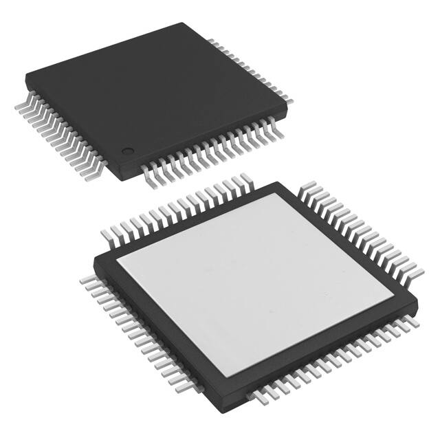
• Currently Available in an HTQFP-64
PowerPAD™ package
234
SUPPORTS DEFENSE, AEROSPACE,
AND MEDICAL APPLICATIONS
•
•
•
•
•
•
•
(1)
Controlled Baseline
One Assembly/Test Site
One Fabrication Site
Available in Military (–55°C/125°C)
Temperature Range (1)
Extended Product Life Cycle
Extended Product-Change Notification
Product Traceability
APPLICATIONS
•
•
•
•
Vibration/Modal Analysis
Multi-Channel Data Acquisition
Acoustics/Dynamic Strain Gauges
Pressure Sensors
xxxx
DESCRIPTION
Based on the single-channel ADS1271, the ADS1278
(octal) is a 24-bit, delta-sigma (ΔΣ) analog-to-digital
converter (ADC) with data rates up to 128 k samples
per second (SPS), allowing simultaneous sampling of
eight channels.
Traditionally, industrial delta-sigma ADCs offering
good drift performance use digital filters with large
passband droop. As a result, they have limited signal
bandwidth and are mostly suited for dc
measurements. High-resolution ADCs in audio
applications offer larger usable bandwidths, but the
offset and drift specifications are significantly weaker
than respective industrial counterparts. The ADS1278
combines these types of converters, allowing highprecision industrial measurement with excellent dc
and ac specifications.
The
high-order,
chopper-stabilized
modulator
achieves very low drift with low in-band noise. The
onboard decimation filter suppresses modulator and
signal out-of-band noise. These ADCs provide a
usable signal bandwidth up to 90% of the Nyquist
rate with less than 0.005 dB of ripple.
Four operating modes allow for optimization of speed,
resolution, and power. All operations are controlled
directly by pins; there are no registers to program.
The device is fully specified over the military
temperature range (–55°C to 125°C) and is available
in an HTQFP-64 PowerPAD package.
Additional temperature ranges are available - contact factory
1
2
3
4
Please be aware that an important notice concerning availability, standard warranty, and use in critical applications of
Texas Instruments semiconductor products and disclaimers thereto appears at the end of this data sheet.
PowerPAD is a trademark of Texas Instruments.
SPI is a trademark of Motorola, Inc.
All other trademarks are the property of their respective owners.
PRODUCTION DATA information is current as of publication date.
Products conform to specifications per the terms of the Texas
Instruments standard warranty. Production processing does not
necessarily include testing of all parameters.
Copyright © 2012, Texas Instruments Incorporated
�ADS1278-EP
SBAS579 – AUGUST 2012
www.ti.com
VREFP VREFN AVDD
Input1
DS
Input2
DS
Input3
DS
Input4
DS
Input5
DS
Input6
DS
Input7
DS
Input8
DS
DVDD
IOVDD
SPI
and
FrameSync
Interface
DRDY/FSYNC
SCLK
DOUT[8:1]
DIN
Control
Logic
TEST[1:0]
FORMAT[2:0]
CLK
SYNC
PWDN[8:1]
CLKDIV
MODE[1:0]
Eight
Digital
Filters
AGND
DGND
ADS1278
This integrated circuit can be damaged by ESD. Texas Instruments recommends that all integrated circuits be handled with
appropriate precautions. Failure to observe proper handling and installation procedures can cause damage.
ESD damage can range from subtle performance degradation to complete device failure. Precision integrated circuits may be more
susceptible to damage because very small parametric changes could cause the device not to meet its published specifications.
ORDERING INFORMATION (1)
TA
–55°C to 125°C
(1)
2
PACKAGE
TQFP - PAP
Reel of 250
ORDERABLE PART NUMBER
TOP-SIDE MARKING
VID NUMBER
ADS1278MPAPTEP
ADS1278EP
V62/12611-01XE
For the most current package and ordering information, see the Package Option Addendum at the end of this document, or see the TI
website at www.ti.com.
Submit Documentation Feedback
Copyright © 2012, Texas Instruments Incorporated
Product Folder Links: ADS1278-EP
�ADS1278-EP
www.ti.com
SBAS579 – AUGUST 2012
PIN ASSIGNMENTS
VREFP
AGND
AVDD
AINN5
AINP5
AINN6
AINP6
54
53
52
51
50
49
VREFN
57
VCOM
AGND
58
55
AGND
59
56
AINP4
AVDD
AINN4
62
60
AINP3
63
61
AINN3
64
PAP PACKAGE
TQFP-64
(TOP VIEW)
AINP2
1
48
AINN7
AINN2
2
47
AINP7
AINP1
3
46
AINN8
AINN1
4
45
AINP8
AVDD
5
44
AVDD
AGND
6
43
AGND
DGND
7
42
PWDN1
TEST0
8
41
PWDN2
TEST1
9
40
PWDN3
CLKDIV
10
39
PWDN4
SYNC
11
38
PWDN5
DIN
12
37
PWDN6
DOUT8
13
36
PWDN7
DOUT7
14
35
PWDN8
DOUT6
15
34
MODE0
DOUT5
16
33
MODE1
ADS1278
27
28
29
30
31
CLK
SCLK
DRDY/FSYNC
FORMAT2
FORMAT1
32
26
DVDD
FORMAT0
24
25
DGND
23
IOVDD
DGND
22
21
DGND
IOVDD
19
20
DOUT1
18
DOUT3
DOUT2
17
DOUT4
(PowerPAD Outline)
Table 1. PIN DESCRIPTIONS
PIN
NAME
NO.
FUNCTION
AGND
6, 43, 54,
58, 59
DESCRIPTION
Analog ground
AINP1
3
Analog input
AINP2
1
Analog input
AINP3
63
Analog input
AINP4
61
Analog input
AINP5
51
Analog input
AINP6
49
Analog input
AINP7
47
Analog input
AINP8
45
Analog input
Analog ground; connect to DGND using a single plane.
AINP[8:1] Positive analog input, channels 8 through 1.
Submit Documentation Feedback
Copyright © 2012, Texas Instruments Incorporated
Product Folder Links: ADS1278-EP
3
�ADS1278-EP
SBAS579 – AUGUST 2012
www.ti.com
Table 1. PIN DESCRIPTIONS (continued)
PIN
4
NAME
NO.
FUNCTION
DESCRIPTION
AINN1
4
Analog input
AINN2
2
Analog input
AINN3
64
Analog input
AINN4
62
Analog input
AINN5
52
Analog input
AINN6
50
Analog input
AINN7
48
Analog input
AINN8
46
Analog input
AVDD
5, 44, 53, 60
Analog power supply
VCOM
55
Analog output
VREFN
57
Analog input
Negative reference input.
VREFP
56
Analog input
Positive reference input.
CLK
27
Digital input
Master clock input (fCLK).
CLKDIV
10
Digital input
DGND
7, 21, 24, 25
Digital ground
AINN[8:1] Negative analog input, channels 8 through 1.
Analog power supply (4.75V to 5.25V).
AVDD/2 Unbuffered voltage output.
CLK input divider control:
1 = 37MHz (High-Speed mode)/otherwise 27MHz
0 = 13.5MHz (low-power)/5.4MHz (low-speed)
Digital ground power supply.
DIN
12
Digital input
Daisy-chain data input.
DOUT1
20
Digital output
DOUT1 is TDM data output (TDM mode).
DOUT2
19
Digital output
DOUT3
18
Digital output
DOUT4
17
Digital output
DOUT5
16
Digital output
DOUT6
15
Digital output
DOUT7
14
Digital output
DOUT8
13
Digital output
DRDY/
FSYNC
29
Digital input/output
DOUT[8:1] Data output for channels 8 through 1.
DVDD
26
Digital power supply
FORMAT0
32
Digital input
FORMAT1
31
Digital input
Frame-Sync protocol: frame clock input; SPI protocol: data ready output.
Digital core power supply.
FORMAT[2:0] Selects Frame-Sync/SPI protocol, TDM/discrete data outputs,
fixed/dynamic position TDM data, and modulator mode/normal operating mode.
FORMAT2
30
Digital input
IOVDD
22, 23
Digital power supply
MODE0
34
Digital input
MODE1
33
Digital input
PWDN1
42
Digital input
PWDN2
41
Digital input
PWDN3
40
Digital input
PWDN4
39
Digital input
PWDN5
38
Digital input
PWDN6
37
Digital input
PWDN7
36
Digital input
PWDN8
35
Digital input
SCLK
28
Digital input/output
I/O power supply (+1.65V to +3.6V).
MODE[1:0] Selects High-Speed, High-Resolution, Low-Power, or Low-Speed
mode operation.
PWDN[8:1] Power-down control for channels 8 through 1.
Serial clock input, Modulator clock output.
SYNC
11
Digital input
Synchronize input (all channels).
TEST0
8
Digital input
TEST[1:0] Test mode select:
TEST1
9
Digital input
Submit Documentation Feedback
00 = Normal operation
11 = Test mode
01 = Do not use
10 = Do not use
Copyright © 2012, Texas Instruments Incorporated
Product Folder Links: ADS1278-EP
�ADS1278-EP
www.ti.com
SBAS579 – AUGUST 2012
ABSOLUTE MAXIMUM RATINGS
Over operating free-air temperature range, unless otherwise noted (1)
UNIT
AVDD to AGND
–0.3 to 6.0
V
DVDD, IOVDD to DGND
–0.3 to 3.6
V
AGND to DGND
–0.3 to 0.3
V
100
mA
Momentary
Input current
10
mA
Analog input to AGND
Continuous
–0.3 to AVDD + 0.3
V
Digital input or output to DGND
–0.3 to DVDD + 0.3
V
150
°C
–60 to 150
°C
Maximum junction temperature, TJ
Storage temperature range
(1)
Stresses above these ratings may cause permanent damage. Exposure to absolute maximum conditions for extended periods may
degrade device reliability. These are stress ratings only, and functional operation of the device at these or any other conditions beyond
those specified is not implied.
THERMAL INFORMATION
ADS1278
THERMAL METRIC (1)
PAP
UNITS
64 PINS
θJA
Junction-to-ambient thermal resistance (2)
33.1
θJC
Junction-to-case thermal resistance
6.2
θJB
Junction-to-board thermal resistance (3)
7.9
ψJT
Junction-to-top characterization parameter (4)
0.2
ψJB
Junction-to-board characterization parameter (5)
7.8
(1)
(2)
(3)
(4)
(5)
°C/W
For more information about traditional and new thermal metrics, see the IC Package Thermal Metrics application report, SPRA953.
The junction-to-ambient thermal resistance under natural convection is obtained in a simulation on a JEDEC-standard, high-K board, as
specified in JESD51-7, in an environment described in JESD51-2a.
The junction-to-board thermal resistance is obtained by simulating in an environment with a ring cold plate fixture to control the PCB
temperature, as described in JESD51-8.
The junction-to-top characterization parameter, ψJT, estimates the junction temperature of a device in a real system and is extracted
from the simulation data for obtaining θJA, using a procedure described in JESD51-2a (sections 6 and 7).
The junction-to-board characterization parameter, ψJB, estimates the junction temperature of a device in a real system and is extracted
from the simulation data for obtaining θJA , using a procedure described in JESD51-2a (sections 6 and 7).
Submit Documentation Feedback
Copyright © 2012, Texas Instruments Incorporated
Product Folder Links: ADS1278-EP
5
�ADS1278-EP
SBAS579 – AUGUST 2012
www.ti.com
ELECTRICAL CHARACTERISTICS
All specifications at TA = –55°C to 125°C, AVDD = 5 V, DVDD = 1.8 V, IOVDD = 3.3 V, fCLK = 27 MHz, VREFP = 2.5 V,
VREFN = 0 V, and all channels active, unless otherwise noted.
PARAMETER
TEST CONDITIONS
Operating temperature range, TA
MIN
TYP
-55
MAX
UNIT
125
°C
Analog Inputs
Full-scale input voltage (FSR (1))
Absolute input voltage
AINP or AINN to AGND
Common-mode input voltage (VCM)
Differential input
impedance
VIN = (AINP – AINN)
±VREF
AGND – 0.1
VCM = (AINP + AINN)/2
V
AVDD +
0.1
V
2.5
V
High-Speed mode
14
kΩ
High-Resolution mode
14
kΩ
Low-Power mode
28
kΩ
Low-Speed mode
140
kΩ
DC Performance
Resolution
No missing codes
High-Speed mode
Data rate (fDATA)
24
Bits
fCLK = 32.768MHz (2)
128,000
SPS
fCLK = 27MHz
105,469
SPS (3)
High-Resolution mode
52,734
SPS
Low-Power mode
52,734
SPS
Low-Speed mode
Integral nonlinearity (INL) (4)
10,547
SPS
±0.0003
±0.0014
Offset error
0.25
2
Offset drift
0.8
Gain error
0.1
Gain drift
1.3
Noise
Differential input, VCM = 2.5V
mV
μV/°C
0.5
% FSR
ppm/°C
High-Speed mode
Shorted input
8.5
68
μV, rms
High-Resolution mode
Shorted input
5.5
13
μV, rms
Low-Power mode
Shorted input
8.5
21
μV, rms
Low-Speed mode
Shorted input
8.0
21
μV, rms
Common-mode rejection
fCM = 60Hz
90
AVDD
Power-supply rejection
% FSR (1)
DVDD
fPS = 60Hz
IOVDD
VCOM output voltage
No load
108
dB
80
dB
85
dB
105
dB
AVDD/2
V
AC Performance
f = 1kHz, –0.5dBFS (5)
Crosstalk
High-Speed mode
Signal-to-noise ratio
(SNR) (6) (unweighted)
High-Resolution mode
VREF = 2.5V
110
dB
111
dB
dB
98
106
Low-Speed mode
98
107
VIN = 1kHz, –0.5dBFS
Passband ripple
Passband
–3dB Bandwidth
6
dB
101
VREF = 3V
Spurious-free dynamic range
(3)
(4)
(5)
(6)
(7)
dB
106
Low-Power mode
Total harmonic distortion (THD) (7)
(1)
(2)
–107
88.3
–108
dB
–96
dB
109
dB
±0.005
dB
0.453 fDATA
Hz
0.49 fDATA
Hz
FSR = full-scale range = 2VREF.
fCLK = 32.768MHz max for High-Speed mode, and 27MHz max for all other modes. When fCLK > 27MHz, operation is limited to FrameSync mode and VREF ≤ 2.6V.
SPS = samples per second.
Best fit method.
Worst-case channel crosstalk between one or more channels.
Minimum SNR is ensured by the limit of the DC noise specification.
THD includes the first nine harmonics of the input signal; Low-Speed mode includes the first five harmonics.
Submit Documentation Feedback
Copyright © 2012, Texas Instruments Incorporated
Product Folder Links: ADS1278-EP
�ADS1278-EP
www.ti.com
SBAS579 – AUGUST 2012
ELECTRICAL CHARACTERISTICS (continued)
All specifications at TA = –55°C to 125°C, AVDD = 5 V, DVDD = 1.8 V, IOVDD = 3.3 V, fCLK = 27 MHz, VREFP = 2.5 V,
VREFN = 0 V, and all channels active, unless otherwise noted.
PARAMETER
Stop band attenuation
TEST CONDITIONS
MIN
High-Resolution mode
TYP
All other modes
Settling time (latency)
UNIT
dB
100
High-Resolution mode
0.547 fDATA
127.453
fDATA
Hz
All other modes
0.547 fDATA
63.453
fDATA
Hz
Stop band
Group delay
MAX
95
High-Resolution mode
39/fDATA
s
All other modes
38/fDATA
s
High-Resolution mode
Complete settling
78/fDATA
s
All other modes
Complete settling
76/fDATA
s
Voltage Reference Inputs
Reference input voltage (VREF)
(VREF = VREFP – VREFN)
fCLK = 27MHz
0.5
2.5
3.1
V
fCLK = 32.768MHz (2)
0.5
2.5
2.6
V
V
V
Negative reference input (VREFN)
AGND – 0.1
AGND +
0.1
Positive reference input (VREFP)
VREFN + 0.5
AVDD +
0.1
Reference Input
impedance
High-Speed mode
0.65
kΩ
High-Resolution mode
0.65
kΩ
Low-Power mode
1.3
kΩ
Low-Speed mode
6.5
kΩ
Digital Input/Output (IOVDD = 1.8V to 3.6V)
VIH
0.7 IOVDD
IOVDD
V
DGND
0.3
IOVDD
V
0.8 IOVDD
IOVDD
V
DGND
0.2
IOVDD
V
High-Speed mode (8)
0.1
32.768
MHz
Other modes
0.1
27
MHz
VIL
VOH
IOH = 4mA
VOL
IOL = 4mA
Input leakage
0 < VIN DIGITAL < IOVDD
Master clock rate (fCLK)
±10
μA
Power Supply
AVDD
4.75
5
5.25
V
DVDD
1.65
1.8
1.95
V
IOVDD
1.65
Power-down current
AVDD current
DVDD current
IOVDD current
(8)
3.6
V
AVDD
1
10
μA
DVDD
1
50
μA
IOVDD
1
11
μA
High-Speed mode
97
145
mA
High-Resolution mode
97
145
mA
Low-Power mode
44
64
mA
Low-Speed mode
9
14
mA
High-Speed mode
23
30
mA
High-Resolution mode
16
20
mA
Low-Power mode
12
17
mA
Low-Speed mode
2.5
4.5
mA
High-Speed mode
0.25
1
mA
High-Resolution mode
0.125
0.6
mA
Low-Power mode
0.125
0.6
mA
Low-Speed mode
0.035
0.3
mA
fCLK = 32.768MHz max for High-Speed mode, and 27MHz max for all other modes. When fCLK > 27MHz, operation is limited to FrameSync mode and VREF ≤ 2.6V.
Submit Documentation Feedback
Copyright © 2012, Texas Instruments Incorporated
Product Folder Links: ADS1278-EP
7
�ADS1278-EP
SBAS579 – AUGUST 2012
www.ti.com
ELECTRICAL CHARACTERISTICS (continued)
All specifications at TA = –55°C to 125°C, AVDD = 5 V, DVDD = 1.8 V, IOVDD = 3.3 V, fCLK = 27 MHz, VREFP = 2.5 V,
VREFN = 0 V, and all channels active, unless otherwise noted.
PARAMETER
Power dissipation
TYP
MAX
UNIT
High-Speed mode
TEST CONDITIONS
MIN
530
785
mW
High-Resolution mode
515
765
mW
Low-Power mode
245
355
mW
Low-Speed mode
50
80
mW
TIMING CHARACTERISTICS: SPI FORMAT
tCLK
tCPW
CLK
· · ·
tCPW
tCD
tCONV
DRDY
tSD
tDS
tSCLK
tSPW
SCLK
tSPW
tMSBPD
DOUT
Bit 23 (MSB)
tDOPD
tDOHD
Bit 22
tDIST
Bit 21
tDIHD
DIN
TIMING REQUIREMENTS: SPI FORMAT
For TA = –40°C to 125°C, IOVDD = 1.65 V to 3.6 V, and DVDD = 1.65 V to 1.95 V.
SYMBOL
PARAMETER
tCLK
CLK period (1/fCLK) (1)
MIN
tCPW
CLK positive or negative pulse width
tCONV
Conversion period (1/fDATA) (2)
(3)
Falling edge of CLK to falling edge of DRDY
tDS
(3)
Falling edge of DRDY to rising edge of first SCLK to retrieve data
tSD
tSCLK
15
22
(4)
tSPW
SCLK period
16
tCLK
0.4
SCLK falling edge to new DOUT invalid (hold time)
10
tDOPD
(5) (3)
SCLK falling edge to new DOUT valid (propagation delay)
(1)
(2)
(3)
(4)
(5)
(6)
8
ns
tCLK
SCLK positive or negative pulse width
(6)
ns
1
(5) (3) (6)
tDIHD
tCLK
tCLK
18
tDOHD
tDIST
ns
ns
1
Falling edge of SCLK to rising edge of DRDY
UNIT
ns
2560
DRDY falling edge to DOUT MSB valid (propagation delay)
(3)
MAX
10,000
256
tCD
tMSBPD
TYP
37
ns
32
ns
New DIN valid to falling edge of SCLK (setup time)
6
ns
Old DIN valid to falling edge of SCLK (hold time)
6
ns
fCLK = 27MHz maximum.
Depends on MODE[1:0] and CLKDIV selection. See Table 7 (fCLK/fDATA).
Load on DRDY and DOUT = 20pF.
For best performance, limit fSCLK/fCLK to ratios of 1, 1/2, 1/4, 1/8, etc.
Timing parameters are characerized or guranteed by design for specified temperature but not production tested.
tDOHD (DOUT hold time) and tDIHD (DIN hold time) are specified under opposite worst-case conditions (digital supply voltage and
ambient temperature). Under equal conditions, with DOUT connected directly to DIN, the timing margin is >4ns.
Submit Documentation Feedback
Copyright © 2012, Texas Instruments Incorporated
Product Folder Links: ADS1278-EP
�ADS1278-EP
www.ti.com
SBAS579 – AUGUST 2012
Figure 1. TIMING CHARACTERISTICS: FRAME-SYNC FORMAT
tCPW
tCLK
CLK
tCPW
tCS
tFRAME
tFPW
tFPW
FSYNC
tFS
tSCLK
tSPW
tSF
SCLK
tSPW
tMSBPD
DOUT
Bit 23 (MSB)
tDOHD
Bit 22
tDIST
tDOPD
Bit 21
tDIHD
DIN
TIMING REQUIREMENTS: FRAME-SYNC FORMAT (1)
For TA = –40°C to 125°C, IOVDD = 1.65 V to 3.6 V, and DVDD = 1.65 V to 1.95 V.
SYMBOL
PARAMETER
MIN
All modes
37
TYP
MAX
UNIT
10,000
ns
tCLK
CLK period (1/fCLK)
tCPW
CLK positive or negative pulse width
tCS
Falling edge of CLK to falling edge of SCLK
tFRAME
Frame period (1/fDATA) (2)
tFPW
FSYNC positive or negative pulse width
1
tSCLK
tFS
Rising edge of FSYNC to rising edge of SCLK
5
ns
tSF
Rising edge of SCLK to rising edge of FSYNC
5
ns
High-Speed mode only
(3)
30.5
ns
12
ns
–0.25
0.25
tCLK
256
2560
tCLK
tSCLK
SCLK period
1
tCLK
tSPW
SCLK positive or negative pulse width
0.4
tCLK
10
tDOHD
(4) (5) (6)
SCLK falling edge to old DOUT invalid (hold time)
tDOPD
(4) (6)
SCLK falling edge to new DOUT valid (propagation delay)
tMSBPD
(4)
tDIST
tDIHD
(1)
(2)
(3)
(4)
(5)
(6)
(5)
FSYNC rising edge to DOUT MSB valid (propagation delay)
ns
31
ns
31
ns
New DIN valid to falling edge of SCLK (setup time)
6
ns
Old DIN valid to falling edge of SCLK (hold time)
6
ns
Timing parameters are characerized or guranteed by design for specified temperature but not production tested.
Depends on MODE[1:0] and CLKDIV selection. See Table 7 (fCLK/fDATA).
SCLK must be continuously running and limited to ratios of 1, 1/2, 1/4, and 1/8 of fCLK.
Timing parameters are characerized or guranteed by design for specified temperature but not production tested.
tDOHD (DOUT hold time) and tDIHD (DIN hold time) are specified under opposite worst-case conditions (digital supply voltage and
ambient temperature). Under equal conditions, with DOUT connected directly to DIN, the timing margin is >4 ns.
Load on DOUT = 20 pF.
Submit Documentation Feedback
Copyright © 2012, Texas Instruments Incorporated
Product Folder Links: ADS1278-EP
9
�ADS1278-EP
SBAS579 – AUGUST 2012
www.ti.com
100000000.00
Estimated Life (Hours)
10000000.00
Wirebond Voiding Fail Mode
1000000.00
100000.00
Electromigration Fail Mode
10000.00
80
90
100
110
120
130
140
150
160
170
Continuous T J (°C)
Figure 2. ADS1278 Operating Life Derating and Wirebond Voiding Fail Mode Chart
Notes:
1. See datasheet for absolute maximum and minimum recommended operating conditions.
2. Sillicon operating life design goal is 10 years at 110°C junction temperature.
10
Submit Documentation Feedback
Copyright © 2012, Texas Instruments Incorporated
Product Folder Links: ADS1278-EP
�ADS1278-EP
www.ti.com
SBAS579 – AUGUST 2012
TYPICAL CHARACTERISTICS
At TA = 25°C, High-Speed mode, AVDD = 5 V, DVDD = 1.8 V, IOVDD = 3.3 V, fCLK = 27 MHz, VREFP = 2.5 V, and
VREFN = 0 V, unless otherwise noted.
OUTPUT SPECTRUM
0
OUTPUT SPECTRUM
0
High-Speed Mode
fIN = 1kHz, -0.5dBFS
32,768 Points
-20
-40
-40
Amplitude (dB)
Amplitude (dB)
High-Speed Mode
fIN = 1kHz, -20dBFS
32,768 Points
-20
-60
-80
-100
-60
-80
-100
-120
-120
-140
-140
-160
-160
10
100
1k
Frequency (Hz)
10k
100k
10
100
1k
Frequency (Hz)
Figure 3.
Number of Occurrences
-40
Amplitude (dB)
NOISE HISTOGRAM
25k
High-Speed Mode
Shorted Input
262,144 Points
-20
100k
Figure 4.
OUTPUT SPECTRUM
0
10k
-60
-80
-100
-120
-140
High-Speed Mode
Shorted Input
262,144 Points
20k
15k
10k
5k
-160
35
28
21
OUTPUT SPECTRUM
0
High-Resolution Mode
fIN = 1kHz, -0.5dBFS
32,768 Points
-20
High-Resolution Mode
fIN = 1kHz, -20dBFS
32,768 Points
-40
Amplitude (dB)
-40
Amplitude (dB)
14
Figure 6.
OUTPUT SPECTRUM
-20
7
Output (mV)
Figure 5.
0
0
100k
-7
10k
-14
100
1k
Frequency (Hz)
-21
10
-35
1
-28
0
-180
-60
-80
-100
-60
-80
-100
-120
-120
-140
-140
-160
-160
10
100
1k
Frequency (Hz)
10k
100k
10
Figure 7.
100
1k
Frequency (Hz)
10k
100k
Figure 8.
Submit Documentation Feedback
Copyright © 2012, Texas Instruments Incorporated
Product Folder Links: ADS1278-EP
11
�ADS1278-EP
SBAS579 – AUGUST 2012
www.ti.com
TYPICAL CHARACTERISTICS (continued)
At TA = 25°C, High-Speed mode, AVDD = 5 V, DVDD = 1.8 V, IOVDD = 3.3 V, fCLK = 27 MHz, VREFP = 2.5 V, and
VREFN = 0 V, unless otherwise noted.
OUTPUT SPECTRUM
0
-40
Number of Occurrences
-20
Amplitude (dB)
NOISE HISTOGRAM
25k
High-Resolution Mode
Shorted Input
262,144 Points
-60
-80
-100
-120
-140
High-Resolution Mode
Shorted Input
262,144 Points
20k
15k
10k
5k
OUTPUT SPECTRUM
21.0
24.5
17.5
10.5
14.0
Low-Power Mode
fIN = 1kHz, -20dBFS
32,768 Points
-20
-40
Amplitude (dB)
Amplitude (dB)
3.5
OUTPUT SPECTRUM
0
-40
-60
-80
-100
-60
-80
-100
-120
-120
-140
-140
-160
-160
10
100
1k
Frequency (Hz)
10k
100k
10
100
1k
Frequency (Hz)
Figure 11.
Number of Occurrences
-40
100k
NOISE HISTOGRAM
25k
Low-Power Mode
Shorted Input
262,144 Points
-20
10k
Figure 12.
OUTPUT SPECTRUM
0
Amplitude (dB)
7.0
Figure 10.
Low-Power Mode
fIN = 1kHz, -0.5dBFS
32,768 Points
-20
0
Output (mV)
Figure 9.
0
-3.5
100k
-7.0
10k
-10.5
100
1k
Frequency (Hz)
-17.5
10
-14.0
1
-21.0
0
-180
-24.5
-160
-60
-80
-100
-120
-140
20k
Low-Power Mode
Shorted Input
262,144 Points
15k
10k
5k
32
37
26
21
16
5
11
0
Output (mV)
Figure 13.
12
-5
100k
-11
10k
-16
100
1k
Frequency (Hz)
-26
10
-32
1
-37
0
-180
-21
-160
Figure 14.
Submit Documentation Feedback
Copyright © 2012, Texas Instruments Incorporated
Product Folder Links: ADS1278-EP
�ADS1278-EP
www.ti.com
SBAS579 – AUGUST 2012
TYPICAL CHARACTERISTICS (continued)
At TA = 25°C, High-Speed mode, AVDD = 5 V, DVDD = 1.8 V, IOVDD = 3.3 V, fCLK = 27 MHz, VREFP = 2.5 V, and
VREFN = 0 V, unless otherwise noted.
OUTPUT SPECTRUM
0
OUTPUT SPECTRUM
0
Low-Speed Mode
fIN = 100Hz, -0.5dBFS
32,768 Points
-20
-20
-40
Amplitude (dB)
-40
Amplitude (dB)
Low-Speed Mode
fIN = 100Hz, -20dBFS
32,768 Points
-60
-80
-100
-60
-80
-100
-120
-120
-140
-140
-160
-160
1
10
100
Frequency (Hz)
1k
10k
1
10
100
Frequency (Hz)
Figure 15.
Number of Occurrences
-40
Amplitude (dB)
NOISE HISTOGRAM
25k
Low-Speed Mode
Shorted Input
262,144 Points
-20
10k
Figure 16.
OUTPUT SPECTRUM
0
1k
-60
-80
-100
-120
-140
20k
Low-Speed Mode
Shorted Input
262,144 Points
15k
10k
5k
-160
THD, THD+N (dB)
-20
Output (mV)
Figure 17.
Figure 18.
TOTAL HARMONIC DISTORTION
vs
FREQUENCY
TOTAL HARMONIC DISTORTION
vs
INPUT AMPLITUDE
0
High-Speed Mode
VIN = -0.5dBFS
-20
-40
-60
-80
THD+N
-100
THD
-120
35
28
21
14
7
0
-7
10k
-14
1k
-21
10
100
Frequency (Hz)
THD, THD+N (dB)
0
1
-35
0.1
-28
0
-180
High-Speed Mode
fIN = 1kHz
-40
-60
-80
THD+N
-100
-120
THD
-140
10
100
1k
Frequency (Hz)
10k
100k
-140
-120
Figure 19.
-100
-80
-60
-40
Input Amplitude (dBFS)
-20
0
Figure 20.
Submit Documentation Feedback
Copyright © 2012, Texas Instruments Incorporated
Product Folder Links: ADS1278-EP
13
�ADS1278-EP
SBAS579 – AUGUST 2012
www.ti.com
TYPICAL CHARACTERISTICS (continued)
At TA = 25°C, High-Speed mode, AVDD = 5 V, DVDD = 1.8 V, IOVDD = 3.3 V, fCLK = 27 MHz, VREFP = 2.5 V, and
VREFN = 0 V, unless otherwise noted.
TOTAL HARMONIC DISTORTION
vs
FREQUENCY
THD, THD+N (dB)
-20
0
High-Resolution Mode
VIN = -0.5dBFS
-20
THD, THD+N (dB)
0
TOTAL HARMONIC DISTORTION
vs
INPUT AMPLITUDE
-40
-60
-80
THD+N
-100
THD
-120
-140
10
THD, THD+N (dB)
-20
1k
Frequency (Hz)
10k
THD+N
-120
THD
-100
0
-20
-80
THD+N
-100
THD
100
1k
Frequency (Hz)
10k
-60
-80
THD+N
-100
THD
-140
-120
100k
-100
-80
-60
-40
Input Amplitude (dBFS)
-20
Figure 23.
Figure 24.
TOTAL HARMONIC DISTORTION
vs
FREQUENCY
TOTAL HARMONIC DISTORTION
vs
INPUT AMPLITUDE
0
Low-Speed Mode
VIN = -0.5dBFS
0
-40
0
Low-Speed Mode
THD, THD+N (dB)
-20
-40
-60
-80
THD+N
-100
-40
-60
-80
THD+N
-100
THD
-120
THD
-120
-140
100
1k
10k
-140
-120
Frequency (Hz)
Figure 25.
14
-20
Low-Power Mode
fIN = 1kHz
-120
-140
10
-80
-60
-40
Input Amplitude (dBFS)
TOTAL HARMONIC DISTORTION
vs
INPUT AMPLITUDE
-120
THD, THD+N (dB)
-100
TOTAL HARMONIC DISTORTION
vs
FREQUENCY
-60
-20
-80
Figure 22.
-40
0
-60
Figure 21.
Low-Power Mode
VIN = -0.5dBFS
10
-40
-140
-120
100k
THD, THD+N (dB)
0
100
High-Resolution Mode
fIN = 1kHz
-100
-80
-60
-40
Input Amplitude (dBFS)
-20
0
Figure 26.
Submit Documentation Feedback
Copyright © 2012, Texas Instruments Incorporated
Product Folder Links: ADS1278-EP
�ADS1278-EP
www.ti.com
SBAS579 – AUGUST 2012
TYPICAL CHARACTERISTICS (continued)
At TA = 25°C, High-Speed mode, AVDD = 5 V, DVDD = 1.8 V, IOVDD = 3.3 V, fCLK = 27 MHz, VREFP = 2.5 V, and
VREFN = 0 V, unless otherwise noted.
OFFSET DRIFT HISTOGRAM
300
25 units based on
20°C intervals over the
range -40°C to +105°C.
800
700
Number of Occurrences
350
Number of Occurrences
GAIN DRIFT HISTOGRAM
900
Multi-lot data based on
20°C intervals over the
range -40°C to +105°C.
250
200
150
100
600
500
400
300
200
100
0
0
-10
-9
-8
-7
-6
-5
-4
-3
-2
-1
0
1
2
3
4
5
6
7
8
9
10
50
Outliers: T < -20°C
-15
-14
-13
-12
-11
-10
-9
-8
-7
-6
-5
-4
-3
-2
-1
0
1
2
3
4
5
6
7
8
9
10
11
12
13
14
15
400
Offset Drift (mV/°C)
Gain Drift (ppm/°C)
Figure 27.
Figure 28.
OFFSET WARMUP DRIFT RESPONSE BAND
GAIN WARMUP DRIFT RESPONSE BAND
40
40
ADS1278 High-Speed and High-Resolution Modes
ADS1274/78 High-Speed and High-Resolution Modes
Normalized Gain Error (ppm)
Normalized Offset (mV)
30
ADS1278 Low-Power Mode
20
10
0
-10
-20
ADS1278 Low-Speed Mode
-30
30
ADS1278 Low-Power Mode
20
10
0
-10
-20
ADS1278 Low-Speed Mode
-30
ADS1274 High-Speed and High-Resolution Modes
-40
-40
0
50
100
150
200
250
Time (s)
300
350
400
0
50
100
150
Figure 29.
400
Number of Occurrences
80
30
25
20
15
10
High-Speed Mode
25 Units
70
60
50
40
30
20
5
10
0
0
-4000
-3600
-3200
-2800
-2400
-2000
-1600
-1200
-800
-400
0
400
800
1200
1600
2000
2400
2800
3200
3600
4000
High-Speed Mode
25 Units
Offset (mV)
350
GAIN ERROR HISTOGRAM
90
-1000
-900
-800
-700
-600
-500
-400
-300
-200
-100
0
100
200
300
400
500
600
700
800
900
1000
Number of Occurrences
35
300
Figure 30.
OFFSET ERROR HISTOGRAM
40
200
250
Time (s)
Gain Error (ppm)
Figure 31.
Figure 32.
Submit Documentation Feedback
Copyright © 2012, Texas Instruments Incorporated
Product Folder Links: ADS1278-EP
15
�ADS1278-EP
SBAS579 – AUGUST 2012
www.ti.com
TYPICAL CHARACTERISTICS (continued)
At TA = 25°C, High-Speed mode, AVDD = 5 V, DVDD = 1.8 V, IOVDD = 3.3 V, fCLK = 27 MHz, VREFP = 2.5 V, and
VREFN = 0 V, unless otherwise noted.
CHANNEL GAIN MATCH HISTOGRAM
70
60
50
40
30
20
50
40
30
20
10
10
0
-1500
-1400
-1300
-1200
-1100
-1000
-900
-800
-700
-600
-500
-400
-300
-200
-100
0
100
200
300
400
500
600
700
800
900
1000
1100
1200
1300
1400
1500
0
High-Speed Mode
10 Units
60
80
Number of Occurrences
Number of Occurrences
90
CHANNEL OFFSET MATCH HISTOGRAM
70
High-Speed Mode
10 Units
Channel Gain Match (ppm)
- 1500
- 1400
- 1300
- 1200
- 1100
- 1000
- 900
- 800
- 700
- 600
- 500
- 400
- 300
- 200
- 100
0
100
200
300
400
500
600
700
800
900
1000
1100
1200
1300
1400
1500
100
Channel Offset Match (mV)
Figure 33.
Figure 34.
OFFSET AND GAIN
vs
TEMPERATURE
VCOM VOLTAGE OUTPUT HISTOGRAM
400
18
Offset
300
100
200
100
0
0
-100
-100
-55
-35
-15
5
25
16
14
12
10
8
6
4
Gain
-200
2
0
65
-300
125
-300
45
85
105
AVDD = 5V
25 Units, No Load
2.40
2.41
2.42
2.43
2.44
2.45
2.46
2.47
2.48
2.49
2.50
2.51
2.52
2.53
2.54
2.55
2.56
2.57
2.58
2.59
2.60
-200
Number of Occurrences
400
200
Normalized Gain Error (ppm)
500
300
Normalized Offset (mV)
20
600
Temperature (°C)
SAMPLING MATCH ERROR HISTOGRAM
REFERENCE INPUT DIFFERENTIAL
IMPEDANCE
vs
TEMPERATURE
40
30 units over 3 production lots,
inter-channel combinations.
Number of Occurrences
35
30
25
20
15
10
5
0.68
6.8
0.67
6.7
0.66
6.6
0.65
6.5
0.64
6.4
High Speed and
High Resolution
6.3
0.63
Low Speed Mode
700
600
650
500
550
400
450
300
350
200
250
100
150
0.62
50
0
Reference Input Impedance (kW)
Figure 36.
Reference Input Impedance (kW)
VCOM Voltage Output (V)
Figure 35.
-55
-40
-20
0
25
45
65
85
105
6.2
125
Temperature (°C)
Sampling Match Error (ps)
Figure 37.
16
Figure 38.
Submit Documentation Feedback
Copyright © 2012, Texas Instruments Incorporated
Product Folder Links: ADS1278-EP
�ADS1278-EP
www.ti.com
SBAS579 – AUGUST 2012
TYPICAL CHARACTERISTICS (continued)
At TA = 25°C, High-Speed mode, AVDD = 5 V, DVDD = 1.8 V, IOVDD = 3.3 V, fCLK = 27 MHz, VREFP = 2.5 V, and
VREFN = 0 V, unless otherwise noted.
28.6
14.2
28.4
14.1
28.2
14
28
13.9
27.8
13.8
27.6
13.7
27.4
High Speed and
High Resolution
13.6
27.2
13.5
27
13.4
26.8
13.3
26.6
Low Power Mode
13.2
13.1
170
Low-Speed Mode
160
Analog Input Impedance (kW)
14.3
ANALOG INPUT DIFFERENTIAL IMPEDANCE
vs
TEMPERATURE
Analog Input Impedance (kW)
Analog Input Impedance (kW)
ANALOG INPUT DIFFERENTIAL IMPEDANCE
vs
TEMPERATURE
150
140
130
120
26.4
-55
-35
-15
5
25
45
65
Temperature (°C)
85
105
110
26.2
125
-55
-35
-15
5
25
45
65
85
105
125
Temperature (°C)
Figure 39.
Figure 40.
INTEGRAL NONLINEARITY
vs
TEMPERATURE
LINEARITY ERROR
vs
INPUT LEVEL
10
10
8
6
Linearity Error (ppm)
INL (ppm of FSR)
8
6
4
4
2
T = +105°C
T = +25°C
0
-2
-4
2
T = -40°C
-6
T = +125°C
-8
-35
-15
5
25
45
65
85
105
-10
-2.5 -2.0 -1.5 -1.0 -0.5
125
Temperature (°C)
1.0
1.5
Figure 41.
Figure 42.
LINEARITY AND TOTAL HARMONIC DISTORTION
vs
REFERENCE VOLTAGE
NOISE AND LINEARITY
vs
INPUT COMMON-MODE VOLTAGE
2.0
2.5
14
14
12
-104
12
12
10
-108
10
THD
8
-112
6
-116
4
Linearity
2
See Electrical Characteristics for VREF Operating Range.
0
0
0.5
1.0
1.5
2.0
VREF (V)
2.5
3.0
3.5
RMS Noise (mV)
-100
THD: fIN = 1kHz, VIN = -0.5dBFS
THD (dB)
Linearity (ppm)
14
0
0.5
VIN (V)
10
Noise
8
8
6
6
Linearity
-120
4
4
-124
2
2
-128
0
-0.5 0
INL (ppm of FSR)
0
-55
0
0.5 1.0 1.5 2.0 2.5 3.0 3.5 4.0 4.5 5.0 5.5
Input Common-Mode Voltage (V)
Figure 43.
Figure 44.
Submit Documentation Feedback
Copyright © 2012, Texas Instruments Incorporated
Product Folder Links: ADS1278-EP
17
�ADS1278-EP
SBAS579 – AUGUST 2012
www.ti.com
TYPICAL CHARACTERISTICS (continued)
At TA = 25°C, High-Speed mode, AVDD = 5 V, DVDD = 1.8 V, IOVDD = 3.3 V, fCLK = 27 MHz, VREFP = 2.5 V, and
VREFN = 0 V, unless otherwise noted.
NOISE
vs
TEMPERATURE
NOISE
vs
REFERENCE VOLTAGE
12
12
Low Power Mode
High Speed Mode
RMS Noise (mV)
10
High-Speed
Low-Power
10
8
Noise (mV)
8
Low Speed Mode
6
Low-Speed
6
4
4
High Resolution Mode
High-Resolution
2
2
See Electrical Characteristics for VREF Operating Range.
0
-55
-35
-15
5
25
45
65
85
105
0
125
0
Temperature (°C)
THD (dB)
2.5
3.0
TOTAL HARMONIC DISTORTION AND NOISE
vs
CLK
COMMON-MODE REJECTION
vs
INPUT FREQUENCY
12
10
8
-60
Noise
6
-80
THD
-100
4
-120
2
0
100M
-140
10k
100k
1M
CLK (Hz)
10M
3.5
0
14
Noise RMS (mV)
-40
1.5
2.0
VREF (V)
Figure 46.
High-Speed Mode
fCLK > 32.768MHz: VREF = 2.048V, DVDD = 2.1V
THD: AIN = fCLK/5120, -0.5dBFS
Noise: Shorted Input
-20
1.0
Figure 45.
Common-Mode Rejection (dB)
0
0.5
-20
-40
-60
-80
-100
-120
10
100
1k
10k
Input Frequency (Hz)
Figure 47.
Figure 48.
POWER-SUPPLY REJECTION
vs
POWER-SUPPLY FREQUENCY
AVDD CURRENT
vs
TEMPERATURE
100k
1M
160
0
High Speed and High Resolution Modes
AVDD Current (mA)
Power-Supply Rejection (dB)
140
-20
-40
-60
AVDD
-80
120
100
80
Low Power Mode
60
40
Low Speed Mode
DVDD
-100
20
IOVDD
-120
10
100
1k
10k
100k
Power-Supply Modulation Frequency (Hz)
1M
0
-55
-35
Figure 49.
18
-15
5
25
45
65
85
105
125
Temperature (°C)
Figure 50.
Submit Documentation Feedback
Copyright © 2012, Texas Instruments Incorporated
Product Folder Links: ADS1278-EP
�ADS1278-EP
www.ti.com
SBAS579 – AUGUST 2012
TYPICAL CHARACTERISTICS (continued)
At TA = 25°C, High-Speed mode, AVDD = 5 V, DVDD = 1.8 V, IOVDD = 3.3 V, fCLK = 27 MHz, VREFP = 2.5 V, and
VREFN = 0 V, unless otherwise noted.
DVDD CURRENT
vs
TEMPERATURE
IOVDD CURRENT
vs
TEMPERATURE
0.5
30
High Speed Mode
0.4
IOVDD Current (mA)
DVDD Current (mA)
25
20
High Resolution Mode
15
10
Low Power Mode
5
Low Speed Mode
0
-55
-35
-15
0.3
High Speed Mode
0.2
High Resolution and Low Power Modes
0.1
Low Speed Mode
5
25
45
65
85
105
0
-55
125
-35
-15
5
25
45
65
85
105
125
Temperature (°C)
Temperature (°C)
Figure 51.
Figure 52.
POWER DISSIPATION
vs
TEMPERATURE
800
Power Dissipation (mW)
700
600
High Speed Mode
500
400
High Resolution Mode
300
Low Power Mode
200
Low Speed Mode
100
0
-55
-35
-15
5
25
45
65
85
105
125
Temperature (°C)
Figure 53.
Submit Documentation Feedback
Copyright © 2012, Texas Instruments Incorporated
Product Folder Links: ADS1278-EP
19
�ADS1278-EP
SBAS579 – AUGUST 2012
www.ti.com
OVERVIEW
High-Speed, High-Resolution, Low-Power, and LowSpeed. Table 2 summarizes the performance of each
mode.
The ADS1278 is an octal 24-bit, delta-sigma ADC
based on the single-channel ADS1271. It offers the
combination of outstanding dc accuracy and superior
ac performance. Figure 54 shows the block diagram.
The converter is comprised of eight advanced, 6thorder, chopper-stabilized, delta-sigma modulators
followed by low-ripple, linear phase FIR filters. The
modulators measure the differential input signal, VIN =
(AINP – AINN), against the differential reference,
VREF = (VREFP – VREFN). The digital filters receive
the modulator signal and provide a low-noise digital
output. To allow tradeoffs among speed, resolution,
and power, four operating modes are supported:
VREFP
AVDD
The ADS1278 is configured by simply setting the
appropriate I/O pins—there are no registers to
program. Data are retrieved over a serial interface
that supports both SPI and Frame-Sync formats. The
ADS1278 has a daisy-chainable output and the ability
to synchronize externally, so it can be used
conveniently in systems requiring more than eight
channels.
DVDD
VREFN
IOVDD
Mod 1
Mod 2
S
R
In High-Speed mode, the maximum data rate is 128
kSPS (when operating at 128 kSPS, Frame-Sync
format must be used). In High-Resolution mode, the
SNR = 111dB (VREF = 3.0 V); in Low-Power mode,
the power dissipation is 31 mW/channel; and in LowSpeed mode, the power dissipation is only 7
mW/channel at 10.5 kSPS. The digital filters can be
bypassed, enabling direct access to the modulator
output.
Modulator
Output
VCOM
VREF
R
AINP1
S
VIN1
AINN1
AINP2
S
VIN2
AINN2
Mod 8
DS
Modulator1
Digital
Filter1
DS
Modulator2
DRDY/FSYNC
SPI
and
Frame-Sync
Interface
SCLK
DOUT [8:1]
DIN
Digital
Filter2
TEST[1:0]
FORMAT[2:0]
CLK
Control
Logic
AINP8
AINN8
S
VIN4/8
DS
Modulator8
SYNC
PWDN [8:1]
Digital
Filter8
CLKDIV
MODE[1:0]
AGND
DGND
Figure 54. Block Diagram
Table 2. Operating Mode Performance Summary
20
MODE
MAX DATA RATE (SPS)
PASSBAND (kHz)
SNR (dB)
NOISE (μVRMS)
POWER/CHANNEL (mW)
High-Speed
128,000
57,984
106
8.5
70
High-Resolution
52,734
23,889
110
5.5
64
Low-Power
52,734
23,889
106
8.5
31
Low-Speed
10,547
4,798
107
8.0
7
Submit Documentation Feedback
Copyright © 2012, Texas Instruments Incorporated
Product Folder Links: ADS1278-EP
�ADS1278-EP
www.ti.com
SBAS579 – AUGUST 2012
FUNCTIONAL DESCRIPTION
SAMPLING APERTURE MATCHING
The ADS1278 is a delta-sigma ADC consisting of
eight independent converters that digitize eight input
signals in parallel.
The ADS1278 converter operates from the same CLK
input. The CLK input controls the timing of the
modulator sampling instant. The converter is
designed such that the sampling skew, or modulator
sampling aperture match between channels, is
controlled. Furthermore, the digital filters are
synchronized to start the convolution phase at the
same modulator clock cycle. This design results in
excellent phase match among the ADS1278
channels.
The converter is composed of two main functional
blocks to perform the ADC conversions: the
modulator and the digital filter. The modulator
samples the input signal together with sampling the
reference voltage to produce a 1s density output
stream. The density of the output stream is
proportional to the analog input level relative to the
reference voltage. The pulse stream is filtered by the
internal digital filter where the output conversion
result is produced.
In operation, the input signal is sampled by the
modulator at a high rate (typically 64x higher than the
final output data rate). The quantization noise of the
modulator is moved to a higher frequency range
where the internal digital filter removes it.
Oversampling results in very low levels of noise
within the signal passband.
Since the input signal is sampled at a very high rate,
input signal aliasing does not occur until the input
signal frequency is at the modulator sampling rate.
This architecture greatly relaxes the requirement of
external antialiasing filters because of the high
modulator sampling rate.
Figure 37 shows the inter-device channel sample
matching for the ADS1278.
FREQUENCY RESPONSE
The digital filter sets the overall frequency response.
The filter uses a multi-stage FIR topology to provide
linear phase with minimal passband ripple and high
stop band attenuation. The filter coefficients are
identical to the coefficients used in the ADS1271. The
oversampling ratio of the digital filter (that is, the ratio
of the modulator sampling to the output data rate, or
fMOD/fDATA) is a function of the selected mode, as
shown in Table 3.
Table 3. Oversampling Ratio versus Mode
MODE SELECTION
OVERSAMPLING RATIO (fMOD/fDATA)
High-Speed
64
High-Resolution
128
Low-Power
64
Low-Speed
64
Submit Documentation Feedback
Copyright © 2012, Texas Instruments Incorporated
Product Folder Links: ADS1278-EP
21
�ADS1278-EP
SBAS579 – AUGUST 2012
www.ti.com
High-Speed, Low-Power, and Low-Speed Modes
0
-1
-2
Amplitude (dB)
The digital filter configuration is the same in HighSpeed, Low-Power, and Low-Speed modes with the
oversampling ratio set to 64. Figure 55 shows the
frequency response in High-Speed, Low-Power, and
Low-Speed modes normalized to fDATA. Figure 56
shows the passband ripple. The transition from
passband to stop band is shown in Figure 57. The
overall frequency response repeats at 64x multiples
of the modulator frequency fMOD, as shown in
Figure 58.
-3
-4
-5
-6
-7
-8
-9
-10
0.45
0
0.47
-20
Amplitude (dB)
0.49
0.51
0.53
0.55
Normalized Input Frequency (fIN/fDATA)
Figure 57. Transition Band Response for HighSpeed, Low-Power, and Low-Speed Modes
-40
-60
-80
20
-100
0
-120
-20
0
0.2
0.6
0.4
0.8
1.0
Normalized Input Frequency (fIN/fDATA)
Figure 55. Frequency Response for High-Speed,
Low-Power, and Low-Speed Modes
Gain (dB)
-40
-140
-60
-80
-100
-120
-140
-160
0.02
0
16
32
48
64
Input Frequency (fIN/fDATA)
Amplitude (dB)
0
Figure 58. Frequency Response Out to fMOD for
High-Speed, Low-Power, and Low-Speed Modes
-0.02
-0.04
-0.06
-0.08
-0.10
0
0.1
0.2
0.3
0.4
0.5
0.6
Normalized Input Frequency (fIN/fDATA)
Figure 56. Passband Response for High-Speed,
Low-Power, and Low-Speed Modes
These image frequencies, if present in the signal and
not externally filtered, will fold back (or alias) into the
passband, causing errors. The stop band of the
ADS1278 provides 100 dB attenuation of frequencies
that begin just beyond the passband and continue out
to fMOD. Placing an antialiasing, low-pass filter in front
of the ADS1278 inputs is recommended to limit
possible high-amplitude, out-of-band signals and
noise. Often, a simple RC filter is sufficient. Table 4
lists the image rejection versus external filter order.
Table 4. Antialiasing Filter Order Image Rejection
22
IMAGE REJECTION (dB)
(f–3dB at fDATA)
ANTIALIASING
FILTER ORDER
HS, LP, LS
HR
1
39
45
2
75
87
3
111
129
Submit Documentation Feedback
Copyright © 2012, Texas Instruments Incorporated
Product Folder Links: ADS1278-EP
�ADS1278-EP
www.ti.com
SBAS579 – AUGUST 2012
High-Resolution Mode
0
-1
-2
Amplitude (dB)
The oversampling ratio is 128 in High-Resolution
mode. Figure 59 shows the frequency response in
High-Resolution mode normalized to fDATA. Figure 60
shows the passband ripple, and the transition from
passband to stop band is shown in Figure 61. The
overall frequency response repeats at multiples of the
modulator frequency fMOD (128 × fDATA), as shown in
Figure 62. The stop band of the ADS1278 provides
100 dB attenuation of frequencies that begin just
beyond the passband and continue out to fMOD.
Placing an antialiasing, low-pass filter in front of the
ADS1278 inputs is recommended to limit possible
high-amplitude out-of-band signals and noise. Often,
a simple RC filter is sufficient. Table 4 lists the image
rejection versus external filter order.
-3
-4
-5
-6
-7
-8
-9
-10
0.45
0.47
0.49
0.51
0.53
0.55
Normalized Input Frequency (fIN/fDATA)
Figure 61. Transition Band Response for HighResolution mode
-20
20
-40
0
-60
-20
-40
-80
Gain (dB)
Amplitude (dB)
0
-100
-120
-60
-80
-100
-120
-140
0
0.50
0.25
0.75
1
Normalized Input Frequency (fIN/fDATA)
-140
-160
0
Figure 59. Frequency Response for HighResolution Mode
32
64
96
128
Normalized Input Frequency (fIN/fDATA)
Figure 62. Frequency Response Out to fMOD for
High-Resolution Mode
0.02
Amplitude (dB)
0
-0.02
-0.04
-0.06
-0.08
-0.10
0
0.1
0.2
0.3
0.4
0.5
0.6
Normalized Input Frequency (fIN/fDATA)
Figure 60. Passband Response for HighResolution Mode
Submit Documentation Feedback
Copyright © 2012, Texas Instruments Incorporated
Product Folder Links: ADS1278-EP
23
�ADS1278-EP
SBAS579 – AUGUST 2012
www.ti.com
Table 5. Ideal Output Code versus Input Signal
PHASE RESPONSE
The ADS1278 incorporates a multiple stage, linear
phase digital filter. Linear phase filters exhibit
constant delay time versus input frequency (constant
group delay). This characteristic means the time
delay from any instant of the input signal to the same
instant of the output data is constant and is
independent of input signal frequency. This behavior
results in essentially zero phase errors when
analyzing multi-tone signals.
INPUT SIGNAL VIN
(AINP – AINN)
IDEAL OUTPUT CODE(1)
≥ +VREF
7FFFFFh
) VREF
2 23 * 1
000001h
0
000000h
* VREF
2 23 * 1
FFFFFFh
ǒ2 2* 1Ǔ
v −VREF
SETTLING TIME
As with frequency and phase response, the digital
filter also determines settling time. Figure 63 shows
the output settling behavior after a step change on
the analog inputs normalized to conversion periods.
The X-axis is given in units of conversion. Note that
after the step change on the input occurs, the output
data change very little prior to 30 conversion periods.
The output data are fully settled after 76 conversion
periods for High-Speed and Low-Power modes, and
78 conversion periods for High-Resolution mode.
Final Value
Settling (%)
100
23
23
800000h
(1) Excludes effects of noise, INL, offset, and gain errors.
ANALOG INPUTS (AINP, AINN)
The ADS1278 measures each differential input signal
VIN = (AINP – AINN) against the common differential
reference VREF = (VREFP – VREFN). The most
positive measurable differential input is +VREF, which
produces the most positive digital output code of
7FFFFFh. Likewise, the most negative measurable
differential input is –VREF, which produces the most
negative digital output code of 800000h.
For optimum performance, the inputs of the ADS1278
are intended to be driven differentially. For singleended applications, one of the inputs (AINP or AINN)
can be driven while the other input is fixed (typically
to AGND or 2.5 V). Fixing the input to 2.5 V permits
bipolar operation, thereby allowing full use of the
entire converter range.
Fully Settled Data
at 76 Conversions
(78 Conversions for
High-Resolution mode)
Initial Value
0
0
10
20
30
40
50
60
70
80
Conversions (1/fDATA)
Figure 63. Step Response
–0.1 V < (AINN or AINP) < AVDD + 0.1 V
DATA FORMAT
The ADS1278 outputs 24 bits of data in twos
complement format.
A positive full-scale input produces an ideal output
code of 7FFFFFh, and the negative full-scale input
produces an ideal output code of 800000h. The
output clips at these codes for signals exceeding fullscale. Table 5 summarizes the ideal output codes for
different input signals.
24
While the ADS1278 measures the differential input
signal, the absolute input voltage is also important.
This value is the voltage on either input (AINP or
AINN) with respect to AGND. The range for this
voltage is:
If either input is taken below –0.4 V or above
(AVDD + 0.4 V), ESD protection diodes on the inputs
may turn on. If these conditions are possible, external
Schottky clamp diodes or series resistors may be
required to limit the input current to safe values (see
the Absolute Maximum Ratings table).
The ADS1278 is a very high-performance ADC. For
optimum performance, it is critical that the appropriate
circuitry be used to drive the ADS1278 inputs. See
the Application Information section for several
recommended circuits.
Submit Documentation Feedback
Copyright © 2012, Texas Instruments Incorporated
Product Folder Links: ADS1278-EP
�ADS1278-EP
www.ti.com
SBAS579 – AUGUST 2012
The ADS1278 uses switched-capacitor circuitry to
measure the input voltage. Internal capacitors are
charged by the inputs and then discharged. Figure 64
shows a conceptual diagram of these circuits. Switch
S2 represents the net effect of the modulator circuitry
in discharging the sampling capacitor; the actual
implementation is different. The timing for switches S1
and S2 is shown in Figure 65. The sampling time
(tSAMPLE) is the inverse of modulator sampling
frequency (fMOD) and is a function of the mode, the
CLKDIV input, and CLK frequency, as shown in
Table 6.
S1
9pF
AINN
Zeff = 14kW ´ (6.75MHz/fMOD)
AINN
Figure 66. Effective Input Impedances
VOLTAGE REFERENCE INPUTS
(VREFP, VREFN)
AVDD AGND
AINP
AINP
S2
S1
AGND AVDD
ESD Protection
Figure 64. Equivalent Analog Input Circuitry
The voltage reference for the ADS1278 ADC is the
differential voltage between VREFP and VREFN:
VREF = (VREFP – VREFN). The voltage reference is
common to all channels. The reference inputs use a
structure similar to that of the analog inputs with the
equivalent circuitry on the reference inputs shown in
Figure 67. As with the analog inputs, the load
presented by the switched capacitor can be modeled
with an effective impedance, as shown in Figure 68.
However, the reference input impedance depends on
the number of active (enabled) channels in addition to
fMOD. As a result of the change of reference input
impedance caused by enabling and disabling
channels, the regulation and setting time of the
external reference should be noted, so as not to
affect the readings.
tSAMPLE = 1/fMOD
S1
VREFP
ON
VREFN
OFF
S2
ON
AGND
AGND
AVDD
AVDD
OFF
Figure 65. S1 and S2 Switch Timing for Figure 64
ESD
Protection
Table 6. Modulator Frequency (fMOD) Mode
Selection
MODE SELECTION
CLKDIV
fMOD
High-Speed
1
fCLK/4
High-Resolution
1
fCLK/4
1
fCLK/8
Low-Power
Low-Speed
0
fCLK/4
1
fCLK/40
0
fCLK/8
Figure 67. Equivalent Reference Input Circuitry
VREFP
The average load presented by the switched
capacitor input can be modeled with an effective
differential impedance, as shown in Figure 66. Note
that the effective impedance is a function of fMOD.
Zeff =
VREFN
5.2kW
´ (6.75MHz/fMOD)
N
N = number of active channels.
Figure 68. Effective Reference Impedance
Submit Documentation Feedback
Copyright © 2012, Texas Instruments Incorporated
Product Folder Links: ADS1278-EP
25
�ADS1278-EP
SBAS579 – AUGUST 2012
www.ti.com
ESD diodes protect the reference inputs. To keep
these diodes from turning on, make sure the voltages
on the reference pins do not go below AGND by
more than 0.4 V, and likewise do not exceed AVDD
by 0.4 V. If these conditions are possible, external
Schottky clamp diodes or series resistors may be
required to limit the input current to safe values (see
the Absolute Maximum Ratings table).
Note that the valid operating range of the reference
inputs is limited to the following parameters:
Table 7. Clock Input Options
MODE
SELECTION
MAX fCLK
(MHz)
CLKDIV
fCLK/fDATA
DATA RATE
(SPS)
High-Speed
32.768
1
256
128,000
High-Resolution
27
1
512
52,734
27
1
512
13.5
0
256
27
1
2,560
5.4
0
512
Low-Power
Low-Speed
52,734
10,547
–0.1 V ≤ VREFN ≤ +0.1 V
MODE SELECTION (MODE)
VREFN + 0.5 V ≤ VREFP ≤ AVDD + 0.1 V
The ADS1278 supports four modes of operation:
High-Speed, High-Resolution, Low-Power, and LowSpeed. The modes offer optimization of speed,
resolution, and power. Mode selection is determined
by the status of the digital input MODE[1:0] pins, as
shown in Table 8. The ADS1278 continually monitors
the status of the MODE pin during operation.
CLOCK INPUT (CLK)
The ADS1278 requires a clock input for operation.
The individual converters of the ADS1278 operate
from the same clock input. At the maximum data rate,
the clock input can be either 27 MHz or 13.5 MHz for
Low-Power mode, or 2 7MHz or 5.4 MHz for LowSpeed mode, determined by the setting of the
CLKDIV input. For High-Speed mode, the maximum
CLK input frequency is 32.768 MHz. For HighResolution mode, the maximum CLK input frequency
is 27 MHz. The selection of the external clock
frequency (fCLK) does not affect the resolution of the
ADS1278. Use of a slower fCLK can reduce the power
consumption of an external clock buffer. The output
data rate scales with clock frequency, down to a
minimum clock frequency of fCLK = 100 kHz. Table 7
summarizes the ratio of the clock input frequency
(fCLK) to data rate (fDATA), maximum data rate and
corresponding maximum clock input for the four
operating modes.
As with any high-speed data converter, a high-quality,
low-jitter clock is essential for optimum performance.
Crystal clock oscillators are the recommended clock
source. Make sure to avoid excess ringing on the
clock input; keeping the clock trace as short as
possible, and using a 50-Ω series resistor placed
close to the source end, often helps.
26
Table 8. Mode Selection
MODE[1:0]
MODE SELECTION
MAX fDATA (1)
00
High-Speed
128,000
01
High-Resolution
52,734
10
Low-Power
52,734
11
Low-Speed
10,547
(1) fCLK = 27 MHz max (32.768MHz max in High-Speed mode).
When using the SPI protocol, DRDY is held high after
a mode change occurs until settled (or valid) data are
ready; see Figure 69 and Table 9.
In Frame-Sync protocol, the DOUT pins are held low
after a mode change occurs until settled data are
ready; see Figure 69 and Table 9. Data can be read
from the device to detect when DOUT changes to
logic 1, indicating that the data are valid.
Submit Documentation Feedback
Copyright © 2012, Texas Instruments Incorporated
Product Folder Links: ADS1278-EP
�ADS1278-EP
www.ti.com
SBAS579 – AUGUST 2012
MODE[1:0]
Pins
ADS1278
Mode
Previous
Mode
New Mode
tNDR-SPI
SPI
Protocol
DRDY
New Mode
Valid Data Ready
tNDR-FS
Frame-Sync DOUT
Protocol
New Mode
Valid Data on DOUT
Figure 69. Mode Change Timing
Table 9. New Data After Mode Change
SYMBOL
DESCRIPTION
MIN
tNDR-SPI
Time for new data to be ready (SPI)
tNDR-FS
Time for new data to be ready (Frame-Sync)
SYNCHRONIZATION (SYNC)
The ADS1278 can be synchronized by pulsing the
SYNC pin low and then returning the pin high. When
the pin goes low, the conversion process stops, and
the internal counters used by the digital filter are
reset. When the SYNC pin returns high, the
conversion process restarts. Synchronization allows
the conversion to be aligned with an external event,
such as the changing of an external multiplexer on
the analog inputs, or by a reference timing pulse.
Because the ADS1278 converters operate in parallel
from the same master clock and use the same SYNC
input control, they are always in synchronization with
each other. The aperture match among internal
channels is typically less than 500 ps. However, the
synchronization of multiple devices is somewhat
different. At device power-on, variations in internal
reset thresholds from device to device may result in
uncertainty in conversion timing.
The SYNC pin can be used to synchronize multiple
devices to within the same CLK cycle. Figure 70
illustrates the timing requirement of SYNC and CLK
in SPI format.
127
TYP
MAX
UNITS
129
Conversions (1/fDATA)
128
Conversions (1/fDATA)
See Figure 71 for the Frame-Sync format timing
requirement.
After synchronization, indication of valid data
depends on whether SPI or Frame-Sync format was
used.
In the SPI format, DRDY goes high as soon as SYNC
is taken low; see Figure 70. After SYNC is returned
high, DRDY stays high while the digital filter is
settling. Once valid data are ready for retrieval,
DRDY goes low.
In the Frame-Sync format, DOUT goes low as soon
as SYNC is taken low; see Figure 71. After SYNC is
returned high, DOUT stays low while the digital filter
is settling. Once valid data are ready for retrieval,
DOUT begins to output valid data. For proper
synchronization, FSYNC, SCLK, and CLK must be
established before taking SYNC high, and must then
remain running. If the clock inputs (CLK, FSYNC or
SCLK) are subsequently interrupted or reset, reassert the SYNC pin.
For consistent performance, re-assert SYNC after
device power-on when data first appear.
Submit Documentation Feedback
Copyright © 2012, Texas Instruments Incorporated
Product Folder Links: ADS1278-EP
27
�ADS1278-EP
SBAS579 – AUGUST 2012
www.ti.com
tCSHD
CLK
tSCSU
tSYN
SYNC
tNDR
DRDY
Figure 70. Synchronization Timing (SPI Protocol)
Table 10. SPI Protocol
SYMBOL
DESCRIPTION
MIN
TYP
MAX
UNITS
tCSHD
CLK to SYNC hold time
10
ns
tSCSU
SYNC to CLK setup time
5
ns
tSYN
Synchronize pulse width
1
tNDR
Time for new data to be ready
CLK periods
129
Conversions (1/fDATA)
tCSHD
CLK
tSCSU
tSYN
SYNC
FSYNC
tNDR
Valid Data
DOUT
Figure 71. Synchronization Timing (Frame-Sync Protocol)
Table 11. Frame-Sync Protocol
SYMBOL
28
DESCRIPTION
MIN
TYP
MAX
UNITS
tCSHD
CLK to SYNC hold time
10
tSCSU
SYNC to CLK setup time
5
ns
tSYN
Synchronize pulse width
1
CLK periods
tNDR
Time for new data to be ready
127
Submit Documentation Feedback
ns
128
Conversions (1/fDATA)
Copyright © 2012, Texas Instruments Incorporated
Product Folder Links: ADS1278-EP
�ADS1278-EP
www.ti.com
SBAS579 – AUGUST 2012
POWER-DOWN (PWDN)
The channels of the ADS1278 can be independently
powered down by use of the PWDN inputs. To enter
the power-down mode, hold the respective PWDN pin
low for at least two CLK cycles. To exit power-down,
return the corresponding PWDN pin high. Note that
when all channels are powered down, the ADS1278
enters a microwatt (μW) power state where all
internal biasing is disabled. In this state, the
TEST[1:0] input pins must be driven; all other input
pins can float. The ADS1278 outputs remain driven.
As shown in Figure 72 and Table 12, a maximum of
130 conversion cycles must elapse for SPI interface,
and 129 conversion cycles must elapse for FrameSync, before reading data after exiting power-down.
Data from channels already running are not affected.
The user software can perform the required delay
time in any of the following ways:
1. Count the number of data conversions after
taking the PWDN pin high.
3. Detect for non-zero data in the powered-up
channel.
After powering up one or more channels, the
channels are synchronized to each other. It is not
necessary to use the SYNC pin to synchronize them.
When a channel is powered down in TDM data
format, the data for that channel are either forced to
zero (fixed-position TDM data mode) or replaced by
shifting the data from the next channel into the
vacated data position (dynamic-position TDM data
mode).
In Discrete data format, the data are always forced to
zero. When powering-up a channel in dynamicposition TDM data format mode, the channel data
remain packed until the data are ready, at which time
the data frame is expanded to include the justpowered channel data. See the Data Format section
for details.
2. Delay 129/fDATA or 130/fDATA after taking the
PWDN pins high, then read data.
···
CLK
tPWDN
PWDN
DRDY/FSYNC
···
tNDR
(1)
DOUT
(Discrete Data Output Mode)
Post Power-Up Data
DOUT1
(TDM Mode, Dynamic Position)
Normal Position
Data Shifts Position
Normal Position
DOUT1
(TDM Mode, Fixed Position)
Normal Position
Data Remains in Position
Normal Position
Figure 72. Power-Down Timing
Table 12. Power-Down Timing
SYMBOL
tPWDN
DESCRIPTION
MIN
PWDN pulse width to enter Power-Down mode
TYP
MAX
2
UNITS
CLK periods
tNDR
Time for new data ready (SPI)
129
130
Conversions (1/fDATA)
tNDR
Time for new data ready (Frame-Sync)
128
129
Conversions (1/fDATA)
Submit Documentation Feedback
Copyright © 2012, Texas Instruments Incorporated
Product Folder Links: ADS1278-EP
29
�ADS1278-EP
SBAS579 – AUGUST 2012
www.ti.com
FORMAT[2:0]
Data can be read from the ADS1278 with two
interface protocols (SPI or Frame-Sync) and several
options of data formats (TDM/Discrete and
Fixed/Dynamic data positions). The FORMAT[2:0]
inputs are used to select among the options. Table 13
lists the available options. See the DOUT Modes
section for details of the DOUT Mode and Data
Position.
Table 13. Data Output Format
FORMAT[2:0]
INTERFACE
PROTOCOL
DOUT
MODE
DATA
POSITION
000
SPI
TDM
Dynamic
001
SPI
TDM
Fixed
010
SPI
Discrete
—
011
Frame-Sync
TDM
Dynamic
100
Frame-Sync
TDM
Fixed
101
Frame-Sync
Discrete
—
110
Modulator Mode
—
—
SERIAL INTERFACE PROTOCOLS
Data are retrieved from the ADS1278 using the serial
interface. Two protocols are available: SPI and
Frame-Sync. The same pins are used for both
interfaces: SCLK, DRDY/FSYNC, DOUT[8:1], and
DIN. The FORMAT[2:0] pins select the desired
interface protocol.
Even though the SCLK input has hysteresis, it is
recommended to keep SCLK as clean as possible to
prevent glitches from accidentally shifting the data.
SCLK may be run as fast as the CLK frequency.
SCLK may be either in free-running or stop-clock
operation between conversions. Note that one fCLK is
required after the falling edge of DRDY until the first
rising edge of SCLK. For best performance, limit
fSCLK/fCLK to ratios of 1, 1/2, 1/4, 1/8, etc. When the
device is configured for modulator output, SCLK
becomes the modulator clock output (see the
Modulator Output section).
DRDY/FSYNC (SPI Format)
In the SPI format, this pin functions as the DRDY
output. It goes low when data are ready for retrieval
and then returns high on the falling edge of the first
subsequent SCLK. If data are not retrieved (that is,
SCLK is held low), DRDY pulses high just before the
next conversion data are ready, as shown in
Figure 73. The new data are loaded within one CLK
cycle before DRDY goes low. All data must be shifted
out before this time to avoid being overwritten.
1/fDATA
1/fCLK
DRDY
SCLK
Figure 73. DRDY Timing with No Readback
SPI SERIAL INTERFACE
The SPI-compatible format is a read-only interface.
Data ready for retrieval are indicated by the falling
DRDY output and are shifted out on the falling edge
of SCLK, MSB first. The interface can be daisychained using the DIN input when using multiple
devices. See the Daisy-Chaining section for more
information.
NOTE: The SPI format is limited to a CLK input
frequency of 27 MHz, maximum. For CLK input
operation above 27 MHz (High-Speed mode only),
use Frame-Sync format.
SCLK
The serial clock (SCLK) features a Schmitt-triggered
input and shifts out data on DOUT on the falling
edge. It also shifts in data on the falling edge on DIN
when this pin is being used for daisy-chaining. The
device shifts data out on the falling edge and the user
normally shifts this data in on the rising edge.
30
DOUT
The conversion data are output on DOUT[8:1]. The
MSB data are valid on DOUT[8:1] after DRDY goes
low. Subsequent bits are shifted out with each falling
edge of SCLK. If daisy-chaining, the data shifted in
using DIN appear on DOUT after all channel data
have been shifted out. When the device is configured
for modulator output, DOUT[8:1] becomes the
modulator data output for each channel (see the
Modulator Output section).
DIN
This input is used when multiple ADS1278s are to be
daisy-chained together. The DOUT1 pin of the first
device connects to the DIN pin of the next, etc. It can
be used with either the SPI or Frame-Sync formats.
Data are shifted in on the falling edge of SCLK. When
using only one ADS1278, tie DIN low. See the DaisyChaining section for more information.
Submit Documentation Feedback
Copyright © 2012, Texas Instruments Incorporated
Product Folder Links: ADS1278-EP
�ADS1278-EP
www.ti.com
SBAS579 – AUGUST 2012
FRAME-SYNC SERIAL INTERFACE
DOUT
Frame-Sync format is similar to the interface often
used on audio ADCs. It operates in slave
fashion—the user must supply framing signal FSYNC
(similar to the left/right clock on stereo audio ADCs)
and the serial clock SCLK (similar to the bit clock on
audio ADCs). The data are output MSB first or leftjustified on the rising edge of FSYNC. When using
Frame-Sync format, the FSYNC and SCLK inputs
must be continuously running with the relationships
shown in the Frame-Sync Timing Requirements.
The conversion data are shifted out on DOUT[8:1].
The MSB data become valid on DOUT[8:1] after
FSYNC goes high. The subsequent bits are shifted
out with each falling edge of SCLK. If daisy-chaining,
the data shifted in using DIN appear on DOUT[8:1]
after all channel data have been shifted out. When
the device is configured for modulator output, DOUT
becomes the modulator data output (see the
Modulator Output section).
DIN
SCLK
This input is used when multiple ADS1278s are to be
daisy-chained together. It can be used with either SPI
or Frame-Sync formats. Data are shifted in on the
falling edge of SCLK. When using only one
ADS1278, tie DIN low. See the Daisy-Chaining
section for more information.
The serial clock (SCLK) features a Schmitt-triggered
input and shifts out data on DOUT on the falling
edge. It also shifts in data on the falling edge on DIN
when this pin is being used for daisy-chaining. Even
though SCLK has hysteresis, it is recommended to
keep SCLK as clean as possible to prevent glitches
from accidentally shifting the data. When using
Frame-Sync format, SCLK must run continuously. If it
is shut down, the data readback will be corrupted.
The number of SCLKs within a frame period (FSYNC
clock) can be any power-of-2 ratio of CLK cycles (1,
1/2, 1/4, etc), as long as the number of cycles is
sufficient to shift the data output from all channels
within one frame. When the device is configured for
modulator output, SCLK becomes the modulator
clock output (see the Modulator Output section).
DOUT MODES
For both SPI and Frame-Sync interface protocols, the
data are shifted out either through individual channel
DOUT pins, in a parallel data format (Discrete mode),
or the data for all channels are shifted out, in a serial
format, through a common pin, DOUT1 (TDM mode).
TDM Mode
In TDM (time-division multiplexed) data output mode,
the data for all channels are shifted out, in sequence,
on a single pin (DOUT1). As shown in Figure 74, the
data from channel 1 are shifted out first, followed by
channel 2 data, etc. After the data from the last
channel are shifted out, the data from the DIN input
follow. The DIN is used to daisy-chain the data output
from an additional ADS1278 or other compatible
device. Note that when all channels of the ADS1278
are disabled, the interface is disabled, rendering the
DIN input disabled as well. When one or more
channels of the device are powered down, the data
format of the TDM mode can be fixed or dynamic.
DRDY/FSYNC (Frame-Sync Format)
In Frame-Sync format, this pin is used as the FSYNC
input. The frame-sync input (FSYNC) sets the frame
period, which must be the same as the data rate. The
required number of fCLK cycles to each FSYNC period
depends on the mode selection and the CLKDIV
input. Table 7 indicates the number of CLK cycles to
each frame (fCLK/fDATA). If the FSYNC period is not
the proper value, data readback will be corrupted.
SCLK
DOUT1
1
2
23
24
25
CH1
47
CH2
48
49
71
CH3
72
73
95
96
CH4
97
CH5
167
168
CH7
169
191
CH8
192
193
194
195
DIN
DRDY
(SPI)
FSYNC
(Frame-Sync)
Figure 74. TDM Mode (All Channels Enabled)
Submit Documentation Feedback
Copyright © 2012, Texas Instruments Incorporated
Product Folder Links: ADS1278-EP
31
�ADS1278-EP
SBAS579 – AUGUST 2012
www.ti.com
TDM Mode, Fixed-Position Data
TDM Mode, Dynamic Position Data
In this TDM data output mode, the data position of
the channels remain fixed, regardless of whether the
channels are powered down. If a channel is powered
down, the data are forced to zero but occupy the
same position within the data stream. Figure 75
shows the data stream with channel 1 and channel 3
powered down.
In this TDM data output mode, when a channel is
powered down, the data from higher channels shift
one position in the data stream to fill the vacated data
slot. Figure 76 shows the data stream with channel 1
and channel 3 powered down.
Discrete Data Output Mode
In Discrete data output mode, the channel data are
shifted out in parallel using individual channel data
output pins DOUT[8:1]. After the 24th SCLK, the
channel data are forced to zero. The data are also
forced to zero for powered down channels. Figure 77
shows the discrete data output format.
SCLK
1
DOUT1
2
23
25
24
CH1
47
48
49
CH2
71
72
73
CH3
95
96
97
CH4
167
CH5
168
169
CH7
191
192
193
CH8
194
195
DIN
DRDY
(SPI)
FSYNC
(Frame-Sync)
Figure 75. TDM Mode, Fixed-Position Data (Channels 1 and 3 Shown Powered Down)
SCLK
DOUT1
1
2
CH2
23
24
25
47
CH4
48
49
50
CH5
119
120
CH7
121
143
CH8
144
145
145
146
DIN
DRDY
(SPI)
FSYNC
(Frame- Sync)
Figure 76. TDM Mode, Dynamic Position Data (Channels 1 and 3 Shown Powered Down)
32
Submit Documentation Feedback
Copyright © 2012, Texas Instruments Incorporated
Product Folder Links: ADS1278-EP
�ADS1278-EP
www.ti.com
SBAS579 – AUGUST 2012
SCLK
1
2
22
DOUT1
CH1
DOUT2
CH2
DOUT3
CH3
DOUT4
CH4
DOUT5
CH5
DOUT6
CH6
DOUT7
CH7
DOUT8
CH8
23
24
25
26
DRDY
(SPI)
FSYNC
(Frame-Sync)
Figure 77. Discrete Data Output Mode
Table 14. Maximum Channels in a Daisy-Chain
(fSCLK = fCLK) (continued)
DAISY-CHAINING
Multiple ADS1278s can be daisy-chained together to
output data on a single pin. The DOUT1 data output
pin of one device is connected to the DIN of the next
device. As shown in Figure 78, the DOUT1 pin of
device 1 provides the output data to a controller, and
the DIN of device 2 is grounded. Figure 79 shows the
data format when reading back data.
The maximum number of channels that may be
daisy-chained in this way is limited by the frequency
of fSCLK, the mode selection, and the CLKDIV input.
The frequency of fSCLK must be high enough to
completely shift the data out from all channels within
one fDATA period. Table 14 lists the maximum number
of daisy-chained channels when fSCLK = fCLK.
To increase the number of data channels possible in
a chain, a segmented DOUT scheme may be used,
producing two data streams. Figure 80 illustrates four
ADS1278s, with pairs of ADS1278s daisy-chained
together. The channel data of each daisy-chained
pair are shifted out in parallel and received by the
processor through independent data channels.
(fSCLK = fCLK)
MODE SELECTION
CLKDIV
MAXIMUM NUMBER
OF CHANNELS
High-Speed
1
10
High-Resolution
1
21
1
21
Low-Power
Low-Speed
0
10
1
106
0
21
Whether the interface protocol is SPI or Frame-Sync,
it is recommended to synchronize all devices by tying
the SYNC inputs together. When synchronized in SPI
protocol, it is only necessary to monitor the DRDY
output of one ADS1278.
In Frame-Sync interface protocol, the data from all
devices are ready after the rising edge of FSYNC.
Since DOUT1 and DIN are both shifted on the falling
edge of SCLK, the propagation delay on DOUT1
creates a setup time on DIN. Minimize the skew in
SCLK to avoid timing violations.
Table 14. Maximum Channels in a Daisy-Chain
Submit Documentation Feedback
Copyright © 2012, Texas Instruments Incorporated
Product Folder Links: ADS1278-EP
33
�ADS1278-EP
SBAS579 – AUGUST 2012
www.ti.com
U1
U2
SYNC
CLK
SYNC
SYNC
CLK
CLK
DIN
SCLK
Note:
DOUT1
DRDY
DRDY Output from Device 1
DOUT1
DOUT from Devices 1 and 2
DIN
SCLK
SCLK
The number of chained devices is limited by the SCLK rate and device mode.
Figure 78. Daisy-Chaining of Two Devices, SPI Protocol (FORMAT[2:0] = 000 or 001)
SCLK
1
DOUT1
2
25
CH1, U1
26
49
CH2, U1
50
CH3, U1
73
74
97
CH4, U1
98
CH5, U1
193
194
217
CH1, U2
218
CH2, U2
385
386
DIN2
DRDY
(SPI)
FSYNC
(Frame-Sync)
Figure 79. Daisy-Chain Data Format of Figure 78
SYNC
CLK
Serial Data
Devices 3 and 4
SYNC
SYNC
CLK
DIN
SYNC
CLK
DOUT1
U1
U2
U3
U4
SYNC
CLK
DOUT1
DIN
DIN
CLK
DOUT1
DIN
FSYNC
FSYNC
FSYNC
FSYNC
SCLK
SCLK
SCLK
SCLK
DOUT1
Serial Data
Devices 1 and 2
SCLK
FSYNC
Note:
The number of chained devices is limited by the SCLK rate and device mode.
Figure 80. Segmented DOUT Daisy-Chain, Frame-Sync Protocol (FORMAT[2:0] = 011 or 100)
34
Submit Documentation Feedback
Copyright © 2012, Texas Instruments Incorporated
Product Folder Links: ADS1278-EP
�ADS1278-EP
www.ti.com
SBAS579 – AUGUST 2012
POWER SUPPLIES
space
The ADS1278 has three power supplies: AVDD,
DVDD, and IOVDD. AVDD is the analog supply that
powers the modulator, DVDD is the digital supply that
powers the digital core, and IOVDD is the digital I/O
power supply. The IOVDD and DVDD power supplies
can be tied together if desired (1.8 V). To achieve
rated performance, it is critical that the power
supplies are bypassed with 0.1-μF and 10-μF
capacitors placed as close as possible to the supply
pins. A single 10-μF ceramic capacitor may be
substituted in place of the two capacitors.
space
Figure 81 shows the start-up sequence of the
ADS1278. At power-on, bring up the DVDD supply
first, followed by IOVDD and then AVDD. Check the
power-supply sequence for proper order, including
the ramp rate of each supply. DVDD and IOVDD may
be sequenced at the same time if the supplies are
tied together. Each supply has an internal reset circuit
whose outputs are summed together to generate a
global power-on reset. After the supplies have
exceeded the reset thresholds, 218 fCLK cycles are
counted before the converter initiates the conversion
process. Following the CLK cycles, the data for 129
conversions are suppressed by the ADS1278 to allow
output of fully-settled data. In SPI protocol, DRDY is
held high during this interval. In frame-sync protocol,
DOUT is forced to zero. The power supplies should
be applied before any analog or digital pin is driven.
For consistent performance, assert SYNC after
device power-on when data first appear.
DVDD
IOVDD
AVDD
1V nom
The ADS1278 incorporates a 6th-order, single-bit,
chopper-stabilized modulator followed by a multistage digital filter that yields the conversion results.
The data stream output of the modulator is available
directly, bypassing the internal digital filter. The digital
filter is disabled, reducing the DVDD current, as
shown in Table 15. In this mode, an external digital
filter implemented in an ASIC, FPGA, or similar
device is required. To invoke the modulator output, tie
FORMAT[2:0], as shown in Figure 82. DOUT[8:1]
then becomes the modulator data stream outputs for
each channel and SCLK becomes the modulator
clock output. The DRDY/FSYNC pin becomes an
unused output and can be ignored. The normal
operation of the Frame-Sync and SPI interfaces is
disabled, and the functionality of SCLK changes from
an input to an output, as shown in Figure 82.
Table 15. Modulator Output Clock Frequencies
CLKDIV
MODULATOR
CLOCK OUTPUT
(SCLK)
DVDD (mA)
00
1
fCLK/4
8
01
1
fCLK/4
7
1
fCLK/8
4
0
fCLK/4
4
1
fCLK/40
1
0
fCLK/8
1
MODE
[1:0]
10
11
(1)
1V nom
MODULATOR OUTPUT
(1)
3V nom
DOUT1
DOUT2
(1)
IOVDD
Modulator Data Channel 1
Modulator Data Channel 2
Internal Reset
DIN
CLK
18
2
fCLK
FORMAT0
129 (max)
tDATA
DRDY
(SPI Protocol)
DOUT
(Frame-Sync Protocol)
FORMAT1
DOUT8
FORMAT2
SCLK
Modulator Data Channel 8
Modulator Clock Output
Figure 82. Modulator Output
Valid Data
Figure 81. Start-Up Sequence
Submit Documentation Feedback
Copyright © 2012, Texas Instruments Incorporated
Product Folder Links: ADS1278-EP
35
�ADS1278-EP
SBAS579 – AUGUST 2012
www.ti.com
In modulator output mode, the frequency of the
modulator clock output (SCLK) depends on the mode
selection of the ADS1278. Table 15 lists the
modulator clock output frequency and DVDD current
versus device mode.
Figure 83 shows the timing relationship of the
modulator clock and data outputs.
The data output is a modulated 1s density data
stream. When VIN = +VREF, the 1s density is
approximately 80% and when VIN = –VREF, the 1s
density is approximately 20%.
Modulator
Clock Output
SCLK
Modulator
Data Output
DOUT
(13ns max)
Figure 83. Modulator Output Timing
PIN TEST USING TEST[1:0] INPUTS
The test mode feature of the ADS1278 allows
continuity testing of the digital I/O pins. In this mode,
the normal functions of the digital pins are disabled
and routed to each other as pairs through internal
logic, as shown in Table 16. The pins in the left
column drive the output pins in the right column.
Note: some of the digital input pins become outputs;
these outputs must be accommodated in the design.
The analog input, power supply, and ground pins all
remain connected as normal. The test mode is
engaged by setting the pins TEST [1:0] = 11. For
normal converter operation, set TEST[1:0] = 00. Do
not use '01' or '10'.
36
Table 16. Test Mode Pin Map (TEST[1:0] = 11)
TEST MODE PIN MAP
INPUT PINS
OUTPUT PINS
PWDN1
DOUT1
PWDN2
DOUT2
PWDN3
DOUT3
PWDN4
DOUT4
PWDN5
DOUT5
PWDN6
DOUT6
PWDN7
DOUT7
PWDN8
DOUT8
MODE0
DIN
MODE1
SYNC
FORMAT0
CLKDIV
FORMAT1
FSYNC/DRDY
FORMAT2
SCLK
VCOM OUTPUT
The VCOM pin provides a voltage output equal to
AVDD/2. The intended use of this output is to set the
output common-mode level of the analog input
drivers. The drive capability of the output is limited;
therefore, the output should only be used to drive
high-impedance nodes (> 1 MΩ). In some cases, an
external buffer may be necessary. A 0.1-μF bypass
capacitor is recommended to reduce noise pickup.
Submit Documentation Feedback
OPA350
VCOM » (AVDD/2)
0.1mF
Figure 84. VCOM Output
Copyright © 2012, Texas Instruments Incorporated
Product Folder Links: ADS1278-EP
�ADS1278-EP
www.ti.com
SBAS579 – AUGUST 2012
APPLICATION INFORMATION
To obtain the specified performance from the
ADS1278, the following layout and component
guidelines should be considered.
1. Power Supplies: The device requires three
power supplies for operation: DVDD, IOVDD, and
AVDD. The allowed range for DVDD is 1.65 V to
1.95 V; the range of IOVDD is 1.65 V to 3.6 V;
AVDD is restricted to 4.75 V to 5.25 V. For all
supplies, use a 10-μF tantalum capacitor,
bypassed with a 0.1-μF ceramic capacitor, placed
close to the device pins. Alternatively, a single
10-μF ceramic capacitor can be used. The
supplies should be relatively free of noise and
should not be shared with devices that produce
voltage spikes (such as relays, LED display
drivers, etc.). If a switching power-supply source
is used, the voltage ripple should be low (less
than 2 mV) and the switching frequency outside
the passband of the converter.
2. Ground Plane: A single ground plane connecting
both AGND and DGND pins can be used. If
separate digital and analog grounds are used,
connect the grounds together at the converter.
3. Digital Inputs: It is recommended to sourceterminate the digital inputs to the device with 50Ω series resistors. The resistors should be placed
close to the driving end of digital source
(oscillator, logic gates, DSP, etc.) This placement
helps to reduce ringing on the digital lines (ringing
may lead to degraded ADC performance).
4. Analog/Digital Circuits: Place analog circuitry
(input buffer, reference) and associated tracks
together, keeping them away from digital circuitry
(DSP, microcontroller, logic). Avoid crossing
digital tracks across analog tracks to reduce
noise coupling and crosstalk.
5. Reference Inputs: It is recommended to use a
minimum 10-μF tantalum with a 0.1-μF ceramic
capacitor directly across the reference inputs,
VREFP and VREFN. The reference input should
be driven by a low-impedance source. For best
performance, the reference should have less than
3 μVRMS in-band noise. For references with noise
higher than this level, external reference filtering
may be necessary.
6. Analog Inputs: The analog input pins must be
driven differentially to achieve specified
performance. A true differential driver or
transformer (ac applications) can be used for this
purpose. Route the analog inputs tracks (AINP,
AINN) as a pair from the buffer to the converter
using short, direct tracks and away from digital
tracks. A 1-nF to 10-nF capacitor should be used
directly across the analog input pins, AINP and
AINN. A low-k dielectric (such as COG or film
type) should be used to maintain low THD.
Capacitors from each analog input to ground can
be used. They should be no larger than 1/10 the
size of the difference capacitor (typically 100 pF)
to preserve the ac common-mode performance.
7. Component Placement: Place the power supply,
analog input, and reference input bypass
capacitors as close as possible to the device
pins. This layout is particularly important for
small-value ceramic capacitors. Larger (bulk)
decoupling capacitors can be located farther from
the device than the smaller ceramic capacitors.
Submit Documentation Feedback
Copyright © 2012, Texas Instruments Incorporated
Product Folder Links: ADS1278-EP
37
�PACKAGE OPTION ADDENDUM
www.ti.com
10-Dec-2020
PACKAGING INFORMATION
Orderable Device
Status
(1)
Package Type Package Pins Package
Drawing
Qty
Eco Plan
(2)
Lead finish/
Ball material
MSL Peak Temp
Op Temp (°C)
(3)
Device Marking
(4/5)
(6)
ADS1278MPAPTEP
ACTIVE
HTQFP
PAP
64
250
RoHS & Green
NIPDAU
Level-3-260C-168 HR
-55 to 125
ADS1278EP
V62/12611-01XE
ACTIVE
HTQFP
PAP
64
250
RoHS & Green
NIPDAU
Level-3-260C-168 HR
-55 to 125
ADS1278EP
(1)
The marketing status values are defined as follows:
ACTIVE: Product device recommended for new designs.
LIFEBUY: TI has announced that the device will be discontinued, and a lifetime-buy period is in effect.
NRND: Not recommended for new designs. Device is in production to support existing customers, but TI does not recommend using this part in a new design.
PREVIEW: Device has been announced but is not in production. Samples may or may not be available.
OBSOLETE: TI has discontinued the production of the device.
(2)
RoHS: TI defines "RoHS" to mean semiconductor products that are compliant with the current EU RoHS requirements for all 10 RoHS substances, including the requirement that RoHS substance
do not exceed 0.1% by weight in homogeneous materials. Where designed to be soldered at high temperatures, "RoHS" products are suitable for use in specified lead-free processes. TI may
reference these types of products as "Pb-Free".
RoHS Exempt: TI defines "RoHS Exempt" to mean products that contain lead but are compliant with EU RoHS pursuant to a specific EU RoHS exemption.
Green: TI defines "Green" to mean the content of Chlorine (Cl) and Bromine (Br) based flame retardants meet JS709B low halogen requirements of