Product
Folder
Sample &
Buy
Support &
Community
Tools &
Software
Technical
Documents
ADS5263
SLAS760D – MAY 2011 – REVISED NOVEMBER 2015
ADS5263 Quad Channel 16-Bit, 100-MSPS High-SNR ADC
1 Features
2 Applications
•
•
•
•
•
LVDD
LGND
ADS5263 Block Diagram
ADS5263
IN1B_P
OUT1P
SERIALIZER
OUT1M
IN1A_P
14-Bit
ADC
16-Bit
FE
DIGITAL
IN1A_M
OUT2P
SERIALIZER
16-Bit ADC
OUT2M
IN1B_M
IN4B_P
OUT7P
SERIALIZER
OUT7M
IN4A_P
14-Bit
ADC
16-Bit
FE
DIGITAL
IN4A_M
OUT8P
SERIALIZER
OUT8M
IN4B_M
ADC Clocking
Sync Signal
LCLKP
LCLKM
BIT CLOCK 8X
CLOCK
BUFFER
CLOCKGEN
FRAME CLOCK 1X
ADCLKP
ADCLKM
ADC CONTROL
SCLK
SDOUT
RESETZ
SDATA
SERIAL
INTERFACE
REFERENCE
CSZ
CLKP
CLKM
PDN
•
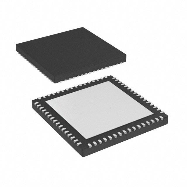
BODY SIZE (NOM)
9.00 mm × 9.00 mm
(1) For all available packages, see the orderable addendum at
the end of the data sheet.
SYNC
•
PACKAGE
VQFN (64)
VCM
•
•
•
•
•
PART NUMBER
ADS5263
REFT
•
Device Information(1)
REFB
•
Using CMOS process technology and innovative
circuit techniques, the ADS5263 is designed to
operate at low power and give very high SNR
performance with a 4-Vpp full-scale input. Using a
low-noise 16-bit front-end stage followed by a 14-bit
ADC, the device gives 85-dBFS SNR up to 10 MHz
and better than 80-dBFS SNR up to 30 MHz.
AGND
•
•
3 Description
INT/EXTZ
•
Medical Imaging – MRI
Spectroscopy
CCD Imaging
AVDD
•
Maximum Sample Rate: 100 MSPS
Programmable Device Resolution
– Quad-Channel, 16-Bit, High-SNR Mode
– Quad-Channel, 14-Bit, Low-Power Mode
16-Bit High-SNR Mode
– 1.4 W Total Power at 100 MSPS
– 355 mW / Channel
– 4 Vpp Full-scale Input
– 85-dBFS SNR at fin = 3 MHz, 100 MSPS
14-Bit Low-Power Mode
– 785 mW Total Power at 100 MSPS
– 195 mW/Channel
– 2-Vpp Full-Scale Input
– 74-dBFS SNR at fin = 10 MHz
– Integrated Clamp (for interfacing to CCD
sensors)
Low-Frequency Noise Suppression
Digital Processing Block
– Programmable FIR Decimation Filters
– Programmable Digital Gain: 0 dB to 12 dB
– 2- or 4-Channel Averaging
Programmable Mapping Between ADC Input
Channels and LVDS Output Pins—Eases Board
Design
Variety of Test Patterns to Verify Data Capture by
FPGA/Receiver
Serialized LVDS Outputs
Internal and External References
3.3-V Analog Supply
1.8-V Digital Supply
Recovers From 6-dB Overload Within 1 Clock
Cycle
Package:
– 9-mm × 9-mm 64-Pin QFN
– Non-Magnetic Package Option for MRI
Systems
CMOS Technology
ISET
1
1
An IMPORTANT NOTICE at the end of this data sheet addresses availability, warranty, changes, use in safety-critical applications,
intellectual property matters and other important disclaimers. PRODUCTION DATA.
�ADS5263
SLAS760D – MAY 2011 – REVISED NOVEMBER 2015
www.ti.com
Table of Contents
1
2
3
4
5
6
7
Features ..................................................................
Applications ...........................................................
Description .............................................................
Revision History.....................................................
Description (continued).........................................
Pin Configuration and Functions .........................
Specifications.........................................................
1
1
1
2
5
6
8
7.1
7.2
7.3
7.4
7.5
Absolute Maximum Ratings ...................................... 8
ESD Ratings.............................................................. 8
Recommended Operating Conditions....................... 8
Thermal Information .................................................. 9
Electrical Characteristics, Dynamic Performance –
16-Bit ADC ................................................................. 9
7.6 Electrical Characteristics, General – 16-Bit ADC
Mode ........................................................................ 10
7.7 Electrical Characteristics, Dynamic Performance –
14-Bit ADC ............................................................... 11
7.8 Digital Characteristics ............................................. 12
7.9 Timing Requirements .............................................. 12
7.10 LVDS Timing at Lower Sampling Frequencies - 2
Wire, 8× Serialization ............................................... 13
7.11 LVDS Timing for 1 Wire 16× Serialization ............ 13
7.12 LVDS Timing for 2 Wire, 7× Serialization ............. 13
7.13 LVDS Timing for 1 Wire, 14× Serialization ........... 13
7.14 Serial Interface Timing Requirements................... 14
7.15 Reset Switching Characteristics ........................... 14
7.16 Typical Characteristics .......................................... 17
8
Detailed Description ............................................ 25
8.1
8.2
8.3
8.4
8.5
8.6
9
Overview .................................................................
Functional Block Diagram .......................................
Feature Description.................................................
Device Functional Modes........................................
Programming ..........................................................
Register Maps .........................................................
25
26
27
41
43
44
Application and Implementation ........................ 62
9.1 Application Information............................................ 62
9.2 Typical Applications ............................................... 70
10 Power Supply Recommendations ..................... 71
11 Layout................................................................... 72
11.1 Layout Guidelines ................................................. 72
11.2 Layout Example .................................................... 73
12 Device and Documentation Support ................. 74
12.1
12.2
12.3
12.4
12.5
Device Support......................................................
Community Resources..........................................
Trademarks ...........................................................
Electrostatic Discharge Caution ............................
Glossary ................................................................
74
75
76
76
76
13 Mechanical, Packaging, and Orderable
Information ........................................................... 76
13.1 Packaging ............................................................. 76
4 Revision History
NOTE: Page numbers for previous revisions may differ from page numbers in the current version.
Changes from Revision C (January 2013) to Revision D
Page
•
Added Register 57 in Register Maps ................................................................................................................................... 45
•
Added Register CB in Register Maps .................................................................................................................................. 45
•
Added Typical Applications section ...................................................................................................................................... 70
•
Added Layout section .......................................................................................................................................................... 72
•
Deleted Ordering Information table. See POA at the end of the data sheet. ...................................................................... 73
Changes from Revision B (October 2011) to Revision C
Page
•
Changed Pin 54 From: REFB To: NC .................................................................................................................................... 7
•
Changed Pin 55 From: REFC To: NC .................................................................................................................................... 7
•
Changed the VCM Pin description To: "Internal reference mode: Outputs the common-mode voltage (1.5 V) that
can be used externally to bias the analog input External reference mode: Apply voltage input that sets the reference
for ADC operation." From: "Outputs the common-mode voltage (1.5 V) that can be used externally to bias the
analog input pins." .................................................................................................................................................................. 7
•
Added "Idle channel noise" To SNR....................................................................................................................................... 9
•
Added "Idle channel noise" To LSB ....................................................................................................................................... 9
•
Changed the INL values- 100 MSPS From: TYP = ±2.2 To: ±5, Added MAX = ±12............................................................. 9
•
to Changed the INL values- 80 MSPS From: TYP = ±2.2 To: ±5 .......................................................................................... 9
•
Added From: VCM common-mode output voltage To: VCM common-mode output voltage, Internal reference mode ..... 10
•
Added From: VCM output current capability To: VCM output current capability, Internal reference mode ......................... 10
2
Submit Documentation Feedback
Copyright © 2011–2015, Texas Instruments Incorporated
Product Folder Links: ADS5263
�ADS5263
www.ti.com
SLAS760D – MAY 2011 – REVISED NOVEMBER 2015
•
Added From: VCM input voltage To: VCM input current, external reference mode............................................................. 10
•
Added VCM input current, external reference mode Typical value - 80 MSPS of 0.5 ......................................................... 10
•
Changed EGREF - 100 MSPS MIN value From: ±2.5 To: ±1.................................................................................................. 10
•
Added Temperature Coefficient to EGREF ............................................................................................................................. 10
•
Added Temperature Coefficient to EGCHAN ........................................................................................................................... 10
•
Changed SNR fin = 5 MHz MIN value From: 68.8 To: to 67.5.............................................................................................. 11
•
Added tA Aperture delay to the Timing Requirements Table................................................................................................ 12
•
Changed From: 2 WIRE, 16× SERIALIZATION To: 2 WIRE, 8× SERIALIZATION ............................................................. 12
•
Added 100 MSPS to the SAMPLING FREQUENCY, MSPS column of LVDS Timing at Lower Sampling Frequencies
- 2 Wire, 8× Serialization ...................................................................................................................................................... 13
•
Changed to 8x from 16x ....................................................................................................................................................... 13
•
Changed LVDS Timing for 2 Wire, 7× Serialization title From: LVDS Timing for 2 Wire, 14× Serialization To: LVDS
Timing for 2 Wire, 7× Serialization ....................................................................................................................................... 13
•
Changed the Digital Filter Section ........................................................................................................................................ 28
•
Changed Table 9 Description From: Reference voltage must be forced on REFT and REFB pins To: Apply voltage
on VCM pin to set the references for ADC operation........................................................................................................... 41
•
Table 10 Added: as bit D4. Added: Register 0x09 to Serial Register Ma; ....................................... 44
•
Table 10 Added: Register bit EXT_REF_VCM. Added: D12 ........................................................ 44
•
Table 10 Added: new register entries from Address 5A to 89. Added: new register F0 ...................................................... 44
•
Added D4 .......................................................................................................................................... 46
•
Added Added register description table (D10 ) for register 0x09.................................................................. 47
•
Added description for register EXT_REF_VCM .................................................................................................................. 54
•
Added Description for , and EXT_REF_VCM .................................................................. 54
•
Added Decsription for 18b SERIALIZATION ........................................................................................................................ 56
•
Changed D11, D10, and D5 To: SERIALIZATION From: SERIAL'N ................................................................................... 56
•
Changed the register for A7-A0 IN HEX............................................................................................................................... 59
•
Added description for register F0 for A7–A0 IN HEX ........................................................................................................... 60
•
Replaced the Clamp Function section with the Clamp Functon for CCD Signals section ................................................... 64
•
Deleted Figure - CCD Sensor Connections ......................................................................................................................... 67
•
Added External Reference Mode ......................................................................................................................................... 68
Changes from Revision A (August 2011) to Revision B
Page
•
Added new Figure below Figure 16...................................................................................................................................... 18
•
Added new Figure below Figure 22 (now Figure 24) ........................................................................................................... 19
•
Added new section below Digital Averaging titled: Performance with Didgital Processing Blocks ...................................... 34
•
Added listitem 6. to the OUTPUT LVDS INTERFACE section............................................................................................. 36
•
Added Added new figure in section Output LVDS Interface (Figure 55).............................................................................. 38
•
Added new section after Output LVDS Interface titled: Programmable LCLK Phase, also 2 new figures added. .............. 40
•
Added register 42 between register 38 and register 45 ...................................................................................................... 54
•
Added new figure 52 in Large and Smll Signal Input Bandwidth section............................................................................. 64
Changes from Original (May 2011) to Revision A
Page
•
Added "Non-Magnetic Package Option for MRI Systems" to Features ................................................................................. 1
•
Changed Features List Item - From: 1.35 W Total Power at 100 MSPS To: 1.4 W Total Power at 100 MSPS.................... 1
•
Changed Features List Item - From: 338 mW / Channel To: 355 mW / Channel .................................................................. 1
•
Changed the CLOCK INPUT values in the ROC table .......................................................................................................... 8
Submit Documentation Feedback
Copyright © 2011–2015, Texas Instruments Incorporated
Product Folder Links: ADS5263
3
�ADS5263
SLAS760D – MAY 2011 – REVISED NOVEMBER 2015
www.ti.com
•
Changed the ELECTRICAL CHARACTERISTICS, DYNAMIC PERFORMANCE – 16-BIT ADC table................................. 9
•
Changed the ELECTRICAL CHARACTERISTICS, GENERAL – 16-BIT ADC MODE table ............................................... 10
•
Added the ELECTRICAL CHARACTERISTICS, DYNAMIC PERFORMANCE – 14-BIT ADC table................................... 11
•
Changed the values in DIGITAL OUTPUTS – LVDS INTERFACE ..................................................................................... 12
•
Added LVDS Timing for 1 Wire 16× Serialization, LVDS Timing for 2 Wire, 7× Serialization, and LVDS Timing for 1
Wire, 14× Serialization.......................................................................................................................................................... 13
•
Added Figure 25, Figure 26, and Figure 27 ......................................................................................................................... 20
•
Added section - Large and Small Signal Input Bandwidth ................................................................................................... 63
•
Added Section - Board Design Considerations .................................................................................................................... 73
•
Added Package Marking ADS5263NM and Ordering Number ADS5263IRGC-NM ............................................................ 73
•
Added Section - DEFINITION OF SPECIFICATIONS ......................................................................................................... 74
•
Added Section - Packaging .................................................................................................................................................. 76
4
Submit Documentation Feedback
Copyright © 2011–2015, Texas Instruments Incorporated
Product Folder Links: ADS5263
�ADS5263
www.ti.com
SLAS760D – MAY 2011 – REVISED NOVEMBER 2015
5 Description (continued)
ADS5263 has a 14-bit low power mode, where it operates as a quad-channel 14-bit ADC. The 16-bit front-end
stage is powered down and the part consumes almost half the power, compared to the 16-bit mode. The 14-bit
mode supports a 2-Vpp full-scale input signal, with typical 74-dBFS SNR. The ADS5263 can be dynamically
switched between the two resolution modes. This allows systems to use the same part in a high-resolution, highpower mode or a low-resolution, low-power mode.
The device also has a digital processing block that integrates several commonly used digital functions, such as
digital gain (up to 12 dB). It includes a digital filter module that has built-in decimation filters (with low-pass, highpass and band-pass characteristics). The decimation rate is also programmable (by 2, by 4, or by 8). This makes
it very useful for narrow-band applications, where the filters can be used to improve SNR and knock-off
harmonics, while at the same time reducing the output data rate.
The device includes an averaging mode where two channels (or even four channels) can be averaged to improve
SNR. A very unique feature is the programmable mapper module that allows flexible mapping between the input
channels and the LVDS output pins. This helps to greatly reduce the complexity of LVDS output routing and can
potentially result in cheaper system boards by reducing the number of PCB layers. Specification of device is over
industrial temperature range of –40°C to 85°C.
Submit Documentation Feedback
Copyright © 2011–2015, Texas Instruments Incorporated
Product Folder Links: ADS5263
5
�ADS5263
SLAS760D – MAY 2011 – REVISED NOVEMBER 2015
www.ti.com
6 Pin Configuration and Functions
RESETZ
SCLK
SDATA
CSZ
AVDD
CLKM
CLKP
AVDD
INT/EXTZ
NC
NC
VCM
SDOUT
ISET
AVDD
SYNC
QFN Package
64-Pin With Thermal Pad
Top View
64
63
62
61
60
59
58
57
56
55
54
53
52
51
50
49
48
IN1A_P
1
IN4A_M
IN1A_M
2
47
IN4A_P
AGND
3
46
AGND
IN1B_P
4
45
IN4B_M
IN1B_M
5
44
IN4B_P
AGND
6
43
AGND
IN2A_P
7
42
IN3A_M
IN2A_M
8
41
IN3A_P
AGND
9
40
AGND
Thermal Pad
64 QFN
LGND
14
35
LVDD
OUT1P
15
34
OUT8M
OUT1M
16
17
18
19
20
21
22
23
24
25
26
27
28
29
30
31
33
32
OUT8P
OUT7M
LGND
OUT7P
36
OUT6M
13
OUT6P
PD
OUT5M
AGND
OUT5P
37
LCLKM
12
LCLKP
LGND
ADCLKM
IN3B_P
ADCLKP
38
OUT4M
11
OUT4P
IN2B_M
OUT3M
IN3B_M
OUT3P
39
OUT2M
10
OUT2P
IN2B_P
P0056-19
Pin Functions
PIN
NAME
NO.
TYPE
DESCRIPTION
ADCLKM
24
O
LVDS frame clock (1X) – negative output
ADCLKP
23
O
LVDS frame clock (1X) – positive output
AGND
3, 6, 9, 37,
40, 43, 46
I
Analog ground
AVDD
50, 57, 60
I
Analog power supply, 3.3 V
CLKM
59
I
Negative differential clock input. For single-ended clock, tie CLKM to ground.
CLKP
58
I
Positive differential clock input
CS
61
I
Serial interface enable input, active LOW. The pin has an internal 300-kΩ pulldown resistor to ground
IN1A_P, IN1A_M
1, 2
I
Differential analog input for channel 1, 16 bit ADC
IN1B_P, IN1B_M
4, 5
I
Differential analog input for channel 1, 14 bit ADC
IN2A_P, IN2A_M
7, 8
I
Differential analog input for channel 2, 16 bit ADC
IN2B_P, IN2B_M
10, 11
I
Differential analog input for channel 2, 14 bit ADC
IN3A_P, IN3A_M
41, 42
I
Differential analog input for channel 3, 16 bit ADC
IN3B_P, IN3B_M
38, 39
I
Differential analog input for channel 3, 14 bit ADC
6
Submit Documentation Feedback
Copyright © 2011–2015, Texas Instruments Incorporated
Product Folder Links: ADS5263
�ADS5263
www.ti.com
SLAS760D – MAY 2011 – REVISED NOVEMBER 2015
Pin Functions (continued)
PIN
NAME
NO.
TYPE
DESCRIPTION
IN4A_P, IN4A_M
47, 48
I
Differential analog input for channel 4, 16 bit ADC
IN4B_P, IN4B_M
44, 45
I
Differential analog input for channel 4, 14 bit ADC
INT/EXT
56
I
Internal/external reference mode select input
Logic HIGH –internal reference
Logic LOW – external reference
ISET
51
I
Bias pin – 56.2 kΩ resistor (1% tolerance value) to ground
LCLKM
26
O
LVDS bit clock (8X) – negative output
LCLKP
25
O
LVDS bit clock (8X) – positive output
LGND
12, 14, 36
I
Digital ground
LVDD
35
I
Digital and I/O power supply, 1.8 V
OUT1P, OUT1M
15, 16
O
Wire 1, channel 1 LVDS differential output
OUT2P, OUT2M
17, 18
O
Wire 2, channel 1 LVDS differential output
OUT3P, OUT3M
19, 20
O
Wire 1, channel 2, LVDS differential output
OUT4P, OUT4M
21, 22
O
Wire 2, channel 2 LVDS differential output
OUT5P, OUT5M
27, 28
O
Wire 1, channel 3 LVDS differential output
OUT6P, OUT6M
29, 30
O
Wire 2, channel 3 LVDS differential output
OUT7P, OUT7M
31, 32
O
Wire 1, channel 4 LVDS differential output
OUT8P, OUT8M
33, 34
O
Wire 2, channel 4 LVDS differential output
PD
13
I
Power-down input
NC
54, 55
Do not connect
RESET
64
I
Serial interface RESET input, active LOW.
When using the serial interface mode, the user must initialize internal registers through hardware
RESET by applying a low-going pulse on this pin or by using software reset option. See the Serial
Interface section.
SCLK
63
I
Serial interface clock input. The pin has an internal 300-kΩ pulldown resistor.
SDATA
62
I
Serial interface data input. The pin has an internal 300-kΩ pulldown resistor.
SDOUT
52
O
Serial register readout
This pin is in the high-impedance state after reset. When the bit is set, the SDOUT pin
becomes active. This is a CMOS digital output running from the AVDD supply.
SYNC
49
I
Input signal to synchronize channels and chips when used with reduced output data rates
Alternate function: Clamp signal input (14-bit ADC mode only)
VCM
53
IO
Internal reference mode: Outputs the common-mode voltage (1.5 V) that can be used externally to bias
the analog input.
External reference mode: Apply voltage input that sets the reference for ADC operation.
Submit Documentation Feedback
Copyright © 2011–2015, Texas Instruments Incorporated
Product Folder Links: ADS5263
7
�ADS5263
SLAS760D – MAY 2011 – REVISED NOVEMBER 2015
www.ti.com
7 Specifications
7.1 Absolute Maximum Ratings
over operating free-air temperature range (unless otherwise noted) (1)
MIN
MAX
UNIT
Supply voltage, AVDD
–0.3
3.9
V
Supply voltage, LVDD
–0.3
2.2
V
Voltage between AGND and DRGND
–0.3
0.3
V
Voltage applied to analog input pins – INP_A, INM_A, INP_B, INM_B
–0.3
minimum (3.6,
AVDD + 0.3 V)
V
Voltage applied to input pins – CLKP, CLKM, RESET, SCLK, SDATA,
CSZ
–0.3
AVDD + 0.3
V
Voltage applied to reference input pins
–0.3
2.8
V
Operating free-air temperature, TA
–40
Operating junction temperature, TJ
Storage temperature, Tstg
(1)
–65
85
°C
125
°C
150
°C
Stresses beyond those listed under Absolute Maximum Ratings may cause permanent damage to the device. These are stress ratings
only, which do not imply functional operation of the device at these or any other conditions beyond those indicated under Recommended
Operating Conditions. Exposure to absolute-maximum-rated conditions for extended periods may affect device reliability.
7.2 ESD Ratings
V(ESD)
(1)
Electrostatic discharge
Human-body model (HBM), per ANSI/ESDA/JEDEC JS-001 (1)
VALUE
UNIT
±2000
V
JEDEC document JEP155 states that 500-V HBM allows safe manufacturing with a standard ESD control process.
7.3 Recommended Operating Conditions
MIN
NOM
MAX
UNIT
3
3.3
3.6
V
1.7
1.8
1.9
V
SUPPLIES
AVDD
Analog supply voltage
LVDD
Digital supply voltage
ANALOG INPUTS
Differential input voltage
16-bit ADC mode
4
VPP
14-bit ADC mode
2
VPP
Input common-mode voltage
Maximum analog input
frequency
1.5 ±0.1
4-Vpp input amplitude, 16-bit ADC mode
70
2-Vpp input amplitude, 16-bit ADC mode
140
V
MHz
CLOCK INPUT
Input clock sample rate
10
Sine wave, ac-coupled
Input clock amplitude differential LVPECL, ac-coupled
(VCLKP-VCLKM)
LVDS, ac-coupled
1.5
VPP
0.2
1.6
VPP
0.2
0.7
VPP
LVCMOS, single-ended, ac-coupled
Input clock duty cycle
100 MSPS
0.2
3.3
35%
50%
V
65%
DIGITAL OUTPUTS
CLOAD
Maximum external load capacitance from each output pin to DRGND
RLOAD
Differential load resistance between the LVDS output pairs (LVDS mode)
Operating free-air temperature, TA
8
–40
Submit Documentation Feedback
5
pF
100
Ω
85
°C
Copyright © 2011–2015, Texas Instruments Incorporated
Product Folder Links: ADS5263
�ADS5263
www.ti.com
SLAS760D – MAY 2011 – REVISED NOVEMBER 2015
7.4 Thermal Information
ADS5263
THERMAL METRIC (1)
RGC (VQFN)
UNIT
64 PINS
RθJA
Junction-to-ambient thermal resistance
20.6
°C/W
RθJC(top)
Junction-to-case (top) thermal resistance
6.1
°C/W
RθJB
Junction-to-board thermal resistance
2.7
°C/W
ψJT
Junction-to-top characterization parameter
0.2
°C/W
ψJB
Junction-to-board characterization parameter
2.6
°C/W
RθJC(bot)
Junction-to-case (bottom) thermal resistance
0.4
°C/W
(1)
For more information about traditional and new thermal metrics, see the Semiconductor and IC Package Thermal Metrics application
report, SPRA953.
7.5 Electrical Characteristics, Dynamic Performance – 16-Bit ADC
Typical values are at 25°C, AVDD = 3.3V, LVDD = 1.8 V, 50% clock duty cycle, –1-dBFS differential analog input (unless
otherwise noted); MIN and MAX values are across the full temperature range TMIN = –40°C to TMAX = 85°C, AVDD = 3.3 V,
LVDD = 1.8 V
PARAMETERS
TEST CONDITIONS
100 MSPS
MIN
TYP
80 MSPS
MAX
MIN
TYP
MAX
UNIT
SNR
Idle channel noise
With inputs tied to common-mode VCM
87.5
87.5
dBFS
LSB
Idle channel noise
With inputs tied to common-mode VCM
0.98
0.98
rms
84.5
85.5
fin = 10 MHz
84.6
85.3
fin = 30 MHz
82.7
83.1
fin = 65 MHz
78.9
79.4
78.2
78.8
77.5
79
74.8
76
71.6
72.5
SNR
Signal-to-noise ratio
fin = 5 MHz at 25°C
81
fin = 5 MHz across temperature
80
fin = 5 MHz
SINAD
fin = 10 MHz
Signal-to-noise and distortion
finn = 30 MHz
ratio
fin = 65 MHz
76.6
dBFS
dBFS
ENOB
Effective number of bits
fin = 5 MHz
12.7
12.8
LSB
DNL
Differential non-linearity
fin = 5 MHz
±0.1
±0.1
LSB
INL
Integrated non-linearity
fin = 5 MHz Changed the INL values 100 MSPS
From: TYP = ±2.2 To: ±5, Added MAX = ±12
±5
LSB
fin = 5 MHz
±5
80
80
fin = 10 MHz
SFDR
Spurious-free dynamic range fin = 30 MHz
80
81
76
77
fin = 65 MHz
74
75
fin = 5 MHz
THD
Total harominc distortion
73.5
±12
78
78.8
fin = 10 MHz
72.5
77.4
79.2
fin = 30 MHz
74.5
76
71.4
72.4
83.5
85
fin = 10 MHz
81
84
fin = 30 MHz
80
83
fin = 65 MHz
75
76
fin = 65 MHz
fin = 5 MHz
HD2
Second harmonic Distortion
73.5
Submit Documentation Feedback
Copyright © 2011–2015, Texas Instruments Incorporated
Product Folder Links: ADS5263
dBc
dBc
dBc
9
�ADS5263
SLAS760D – MAY 2011 – REVISED NOVEMBER 2015
www.ti.com
Electrical Characteristics, Dynamic Performance – 16-Bit ADC (continued)
Typical values are at 25°C, AVDD = 3.3V, LVDD = 1.8 V, 50% clock duty cycle, –1-dBFS differential analog input (unless
otherwise noted); MIN and MAX values are across the full temperature range TMIN = –40°C to TMAX = 85°C, AVDD = 3.3 V,
LVDD = 1.8 V
PARAMETERS
TEST CONDITIONS
Worst Spur
Excluding HD2, HD3
80 MSPS
TYP
73.5
80
80
fin = 10 MHz
80
81
fin = 30 MHz
75
77
fin = 65 MHz
74
75
fin = 5 MHz
80
90
fin = 10 MHz
85
90
finn = 30 MHz
85
88
fin = 5 MHz
HD3
Third harmonic distortion
100 MSPS
MIN
MAX
MIN
TYP
MAX
UNIT
dBc
dBc
fin = 65 MHz
82
86
IMD
2-tone intermodulation
distortion
f1 = 8 MHz, f2 = 10 MHZ, each tone at –7 dBFS
92
92
dBFS
Input overload recovery
Recovery to within 1% (of final value) for 6-dB
overload with sine wave input
1
1
clock
cyles
PSRR
AC power supply rejection
ratio
For 50 mV signal on AVDD supply, up to 1
MHz ripple frequency
30
30
dB
7.6 Electrical Characteristics, General – 16-Bit ADC Mode
Typical values are at 25°C, AVDD = 3.3V, LVDD = 1.8V, 50% clock duty cycle, –1dBFS differential analog input (unless
otherwise noted); MIN and MAX values are across the full temperature range TMIN = –40°C to TMAX = 85°C, AVDD = 3.3V,
LVDD = 1.8V
100 MSPS
PARAMETERS
MIN
80 MSPS
TYP MAX
MIN
TYP MAX
UNIT
ANALOG INPUT
Differential input voltage range (0-dB gain)
Differential input resistance (at dc)
Differential input capacitance
Analog input bandwidth
Analog input common-mode current (per input pin)
VCM common-mode output voltage, Internal reference mode
VCM output current capability, Internal reference mode
VCM input voltage, external reference mode
1.45
VCM input current, external reference mode
4
4
Vpp
2.5
2.5
kΩ
12
12
pF
700
700
MHz
8
8
1.5
1.5
3
3
1.5
1.55
0.5
1.45
1.5
0.5
µA/MSPS
V
mA
1.55
V
mA
DC ACCURACY
Offset error
EGREF
Gain error due to internal reference inaccuracy alone
EGREF
Temperature
Coefficient
Internal reference mode
External l reference mode
EGCHAN
Gain error of channel alone
EGCHAN
Temperature
Coefficient
Gain matching
10
Submit Documentation Feedback
±1
±10
±30
±10
mV
±0.5
1
±0.5
% FS
0.002
0.00
2
Δ%/°C
0.001
0.00
1
Δ%/°C
1
1
% FS
0.002
0.00
2
Δ%/°C
0.5%
0.5%
Copyright © 2011–2015, Texas Instruments Incorporated
Product Folder Links: ADS5263
�ADS5263
www.ti.com
SLAS760D – MAY 2011 – REVISED NOVEMBER 2015
Electrical Characteristics, General – 16-Bit ADC Mode (continued)
Typical values are at 25°C, AVDD = 3.3V, LVDD = 1.8V, 50% clock duty cycle, –1dBFS differential analog input (unless
otherwise noted); MIN and MAX values are across the full temperature range TMIN = –40°C to TMAX = 85°C, AVDD = 3.3V,
LVDD = 1.8V
100 MSPS
PARAMETERS
MIN
80 MSPS
TYP MAX
MIN
TYP MAX
UNIT
POWER SUPPLY
IAVDD
Analog supply current
370
390
290
mA
ILVDD
Digital and output buffer supply current with 100-Ω external
LVDS termination
110
150
100
mA
Analog power
1.22
0.96
W
Digital power
0.2
0.18
Global power down
63
110
63
mW
208
250
208
mW
Standby
W
7.7 Electrical Characteristics, Dynamic Performance – 14-Bit ADC
Typical values are at 25°C, AVDD = 3.3V, LVDD = 1.8 V, 50% clock duty cycle, –1-dBFS differential analog input (unless
otherwise noted); MIN and MAX values are across the full temperature range TMIN = –40°C to TMAX = 85°C, AVDD = 3.3 V,
LVDD = 1.8 V
PARAMETERS
SNR
Signal-to-noise ratio
TEST CONDITIONS
fin = 5 MHz
100 MSPS
MIN
TYP
67.5
74
finv = 30 MHz
73
fin = 65 MHz
SINAD
Signal-to-noise and distortion ratio
fin = 5 MHz
fin = 30 MHz
fin = 30 MHz
HD2
Second harmonic Distortion
HD3
Third harmonic distortion
85
81
fin = 65 MHz
THD
Total harmonic distortion
83.5
fin = 30 MHz
78
fin = 65 MHz
76.5
71.8
84
fin = 65 MHz
80
71.8
81
fin = 65 MHz
78
Submit Documentation Feedback
Product Folder Links: ADS5263
dBc
85
fin = 30 MHz
Copyright © 2011–2015, Texas Instruments Incorporated
dBc
92
fin = 30 MHz
fin = 5 MHz
dBc
78
69
fin = 5 MHz
dBFS
70.3
71.8
fin = 5 MHz
dBFS
73.5
71.9
finn = 65 MHz
SFDR
Spurious-free dynamic range
UNIT
71.3
65.8
fin = 5 MHz
MAX
dBc
11
�ADS5263
SLAS760D – MAY 2011 – REVISED NOVEMBER 2015
www.ti.com
7.8 Digital Characteristics
The DC specifications refer to the condition where the digital outputs are not switching, but are permanently at a valid logic
level 0 or 1. AVDD = 3.3V, LVDD = 1.8V
PARAMETER
TEST CONDITIONS
MIN
TYP MAX
UNIT
DIGITAL INPUTS – RESET, SCLK, SDATA, CS, PDN, SYNC, INT/EXT
All digital inputs support 1.8-V and
3.3-V CMOS logic levels.
VIH
High-level input voltage
VIL
Low-level input voltage
IIH
High-level input
current
SDATA, SCLK, CS
IIL
Low-level input
current
SDATA, SCLK, CS
1.3
V
0.4
(1)
V
VHIGH = 1.8 V
5
μA
VLOW = 0 V
0
μA
DIGITAL CMOS OUTPUT – SDOUT
VOH
High-level output voltage
IOH = 100 µA
AVDD – 0.05
V
VOL
Low-level output voltage
IOL = 100 µA
0.05
V
DIGITAL OUTPUTS – LVDS INTERFACE (OUT1P/M TO OUT8P/M, ADCLKP/M, LCLKP/M)
VODH High-level output differential voltage
With external 100-Ω termination
275
465
mV
VODL Low-level output differential voltage
With external 100-Ω termination
–465
–370 –275
mV
1000
1200 1400
mV
VOCM Output common-mode voltage
(1)
370
CS, SDATA, SCLK have internal 300-kΩ pulldown resistor.
7.9 Timing Requirements (1)
Typical values are at 25°C, AVDD = 3.3 V, LVDD = 1.8 V, sampling frequency = 100 MSPS, sine wave input clock = 1.5 Vpp
clock amplitude, CLOAD = 5 pF (2), RLOAD = 100 Ω (3), unless otherwise noted. MIN and MAX values are across the full
temperature range, TMIN = –40°C to TMAX = 85°C, AVDD = 3.3 V, LVDD = 1.7 V to 1.9 V
MIN
tj
Aperture jitter
tA
Aperture delay
Time delay between rising edge of input clock and the actual
sampling instant
ADC latency
tsu
MAX
220
Wake-up time
2 WIRE, 8× SERIALIZATION
TYP
3
Time to valid data after coming out of STANDBY mode
10
Time to valid data after coming out of global power down
60
Latency of ADC alone, excludes the delay from input clock to
output clock (tPDI), Figure 3
16
UNIT
fs rms
ns
μs
Clock
cycles
(4)
Data setup time
Data valid (5) to zero-crossing of LCLKP
(5)
th
Data hold time
Zero-crossing of LCLKP to data becoming invalid
tPDI
Clock propagation
delay
Input clock rising edge crossover to output frame clock ADCLKP
rising edge crossover, tPDI = (ts/4) + tdelay
Variation of tPDI
Between two devices at same temperature and LVDD supply
LVDS bit clock duty
cycle
Duty cycle of differential clock, (LCLKP-LCLKM)
0.23
ns
0.31
ns
6.8
8.8
±0.6
10.8
ns
ns
50%
tRISE
tFALL
Data rise time,
Data fall time
Rise time measured from –100 mV to 100 mV,
Fall time measured from 100 mV to –100 mV
10 MSPS ≤ Sampling frequency ≤ 100 MSPS
0.17
ns
tCLKRISE
tCLKFALL
Output clock rise time,
Output clock fall time
Rise time measured from –100 mV to 100 mV
Fall time measured from 100 mV to –100 mV
10 MSPS ≤ Sampling frequency ≤ 100 MSPS
0.2
ns
(1)
(2)
(3)
(4)
(5)
12
Timing parameters are ensured by design and characterization and not tested in production.
CLOAD is the effective external single-ended load capacitance between each output pin and ground.
RLOAD is the differential load resistance between the LVDS output pair.
Measurements are done with a transmission line of 100-Ω characteristic impedance between the device and the load. Setup and hold
time specifications take into account the effect of jitter on the output data and clock.
Data valid refers to logic HIGH of 100 mV and logic LOW of –100 mV.
Submit Documentation Feedback
Copyright © 2011–2015, Texas Instruments Incorporated
Product Folder Links: ADS5263
�ADS5263
www.ti.com
SLAS760D – MAY 2011 – REVISED NOVEMBER 2015
7.10 LVDS Timing at Lower Sampling Frequencies - 2 Wire, 8× Serialization
SAMPLING FREQUENCY, MSPS
SETUP TIME
MIN
TYP MAX
HOLD TIME
MIN
TYP
MAX
UNIT
100
0.23
0.31
ns
80
0.47
0.47
ns
65
0.56
0.7
ns
50
0.66
1
ns
20
2.7
2.8
ns
7.11 LVDS Timing for 1 Wire 16× Serialization
SAMPLING FREQUENCY, MSPS
SETUP TIME
MIN
TYP MAX
HOLD TIME
MIN
TYP
MAX
UNIT
65
0.15
0.31
ns
50
0.27
0.35
ns
40
0.45
0.55
ns
20
1.1
1.4
ns
Clock Propagation Delay
tPDI = (ts/8) + tdelay
10 MSPS < Sampling Frequency < 65 MSPS
tdelay
MIN
6.8
ns
TYP MAX
8.8
ns
10.8
ns
7.12 LVDS Timing for 2 Wire, 7× Serialization
SAMPLING FREQUENCY, MSPS
SETUP TIME
MIN
TYP MAX
HOLD TIME
MIN
TYP
MAX
UNIT
100
0.29
0.39
ns
80
0.51
0.60
ns
65
0.58
0.82
ns
50
0.85
1.20
ns
20
3.2
3.3
ns
Clock Propagation Delay
tPDI = (ts/3.5) + tdelay
10 MSPS < Sampling Frequency < 100 MSPS
tdelay
MIN
6.8
ns
TYP MAX
8.8
ns
10.8
ns
7.13 LVDS Timing for 1 Wire, 14× Serialization
SAMPLING FREQUENCY, MSPS
SETUP TIME
MIN
TYP MAX
HOLD TIME
MIN
TYP
MAX
UNIT
65
0.19
0.28
ns
50
0.37
0.42
ns
30
0.70
1.0
ns
20
1.3
1.5
ns
Clock Propagation Delay
tPDI = (ts/7) + tdelay
10 MSPS < Sampling Frequency < 65 MSPS
tdelay
ns
MIN
TYP MAX
ns
6.8
8.8 10.8
ns
Submit Documentation Feedback
Copyright © 2011–2015, Texas Instruments Incorporated
Product Folder Links: ADS5263
13
�ADS5263
SLAS760D – MAY 2011 – REVISED NOVEMBER 2015
www.ti.com
7.14 Serial Interface Timing Requirements
Typical values at 25°C, MIN and MAX values across the full temperature range TMIN = –40°C to TMAX = 85°C, AVDD = 3.3 V,
LVDD = 1.8 V, unless otherwise noted.
MIN
TYP MAX
UNIT
> DC
20
MHz
fSCLK
SCLK frequency (= 1/ tSCLK)
tSLOADS
CS to SCLK setup time
25
ns
tSLOADH
SCLK to CS hold time
25
ns
tDS
SDATA setup time
25
ns
tDH
SDATA hold time
25
ns
7.15 Reset Switching Characteristics
Typical values at 25°C, MIN and MAX values across the full temperature range TMIN = –40°C to TMAX = 85°C (unless
otherwise noted)
PARAMETER
TEST CONDITIONS
MIN
t1
Power-on delay
Delay from power up of AVDD and LVDD to RESET pulse active
t2
Reset pulse duration
Pulse duration of active RESET signal
t3
Register write delay
Delay from RESET disable to CS active
TYP MAX
1
50
UNIT
ms
ns
100
ns
POWER SUPPLY
AVDD,DRVDD
t1
RESET
t2
t3
SEN
NOTE: A high-going pulse on RESET pin is required in serial interface mode in case of initialization through hardware reset.
For parallel interface operation, RESET has to be tied permanently HIGH.
Figure 1. Reset Timing Diagram
14
Submit Documentation Feedback
Copyright © 2011–2015, Texas Instruments Incorporated
Product Folder Links: ADS5263
�ADS5263
www.ti.com
SLAS760D – MAY 2011 – REVISED NOVEMBER 2015
CLKM
CLKM
INPUT
INPUTCLOCK
CLOCK
1X
1X
CLKP
CLKP
ttPDI
PDI
ADCLKM
ADCLKM
FRAME
FRAME CLOCK
CLOCK
0.5X
X
ADCLKP
ADCLKP
ttsusu
t h
th
LCLKM
LCLKM
BIT CLOCK
4X
4X
LCLKP
LCLKP
tsu
OUTPUT DATA
&FRAME CLK
OUT 1, OUT 2
OUT 3, OUT 4
OUT 5, OUT 6
OUT 7, OUT 8
th
Dn *
th h
tsu
Dn +1*
Figure 2. LVDS Timing
Submit Documentation Feedback
Copyright © 2011–2015, Texas Instruments Incorporated
Product Folder Links: ADS5263
15
�ADS5263
SLAS760D – MAY 2011 – REVISED NOVEMBER 2015
www.ti.com
Sample
N + 17
Sample
N + 15
Sample
N + 16
Sample
N
INPUT SIGNAL
INPUT
CLOCK
Freq = fS
tA
CLKM
CLKP
tPDI
LATENCY = 16 Clocks
DCLKP
BIT
CLOCK
Freq = 8 × f S
DCLKM
OUTPUT
DATA
Rate = 16 × fS
OUTM
OUTP
D15 D14 D13 D12 D11 D10
D9
D8
D7
D6
D5
D4
D3
D2
D1
D0 D15 D14 D13 D12 D11 D10
SAMPLE N – 1
FRAME
CLOCK
Freq = 1 × fS
D9
D8
D7
D6
D5
D4
D3
D2
D1
D0
D15 D14
SAMPLE N
ADCLKM
ADCLKP
Figure 3. Latency Diagram
16
Submit Documentation Feedback
Copyright © 2011–2015, Texas Instruments Incorporated
Product Folder Links: ADS5263
�ADS5263
www.ti.com
SLAS760D – MAY 2011 – REVISED NOVEMBER 2015
OUTP
Logic
Logic
0 0
VODL = -350 mV*
Logic 0
VODH = +350 mV*
OUTM
VOCM
GND
GND
*With external 100-W termination
Figure 4. LVDS Output Voltage Levels
7.16 Typical Characteristics
7.16.1 Typical Characteristic – 16-Bit ADC Mode
All plots are at 25°C, AVDD = 3.3 V, LVDD = 1.8 V, maximum-rated sampling frequency, sine-wave input clock = 1.5 VPP
differential clock amplitude, 50% clock duty cycle, –1 dBFS differential analog input, internal reference mode, 0 dB gain, 32k
point FFT (unless otherwise noted).
0
0
SNR = 85.6 dBFS
SINAD = 83.5 dBFS
THD = 86.7 dBc
SFDR = 89.7 dBc
−10
−30
−30
−40
−40
−50
−60
−70
−80
−50
−60
−70
−80
−90
−90
−100
−100
−110
−110
−120
−120
−130
−130
−140
0
5
10
Frequency (MHz)
15
SNR = 84.7 dBFS
SINAD = 81.6 dBFS
SFDR = 84.9 dBc
THD = 83.4 dBc
−20
Amplitude (dBFS)
Amplitude (dBFS)
−20
−10
−140
20
0
5
10
Frequency (MHz)
15
20
G001
Figure 5. FFT for 3-MHz Input Signal, fS = 40 MSPS
G002
Figure 6. FFT for 15-MHz Input Signal, fS = 40 MSPS
0
0
SNR =85.7 dBFS
SINAD = 81.4 dBFS
THD = 82.4 dBc
SFDR = 83.1 dBc
−10
−30
−30
−40
−40
−50
−60
−70
−80
−50
−60
−70
−80
−90
−90
−100
−100
−110
−110
−120
−120
−130
−130
−140
0
5
10
15
20
25
Frequency (MHz)
30
35
SNR = 84.8 dBFS
SINAD = 79.4 dBFS
THD = 79.9 dBc
SFDR = 82.7dBc
−20
Amplitude (dBFS)
Amplitude (dBFS)
−20
−10
40
−140
G003
Figure 7. FFT for 3-MHz Input Signal, fS = 80 MSPS
0
5
10
15
20
25
Frequency (MHz)
30
35
40
G004
Figure 8. FFT for 15-MHz Input Signal, fS = 80 MSPS
Submit Documentation Feedback
Copyright © 2011–2015, Texas Instruments Incorporated
Product Folder Links: ADS5263
17
�ADS5263
SLAS760D – MAY 2011 – REVISED NOVEMBER 2015
www.ti.com
Typical Characteristic – 16-Bit ADC Mode (continued)
All plots are at 25°C, AVDD = 3.3 V, LVDD = 1.8 V, maximum-rated sampling frequency, sine-wave input clock = 1.5 VPP
differential clock amplitude, 50% clock duty cycle, –1 dBFS differential analog input, internal reference mode, 0 dB gain, 32k
point FFT (unless otherwise noted).
0
0
SNR = 78.9 dBFS
SINAD = 73.9 dBFS
THD = 74.6 dBc
SFDR = 77.4 dBc
−10
−20
−30
−30
−40
−40
Amplitude (dBFS)
Amplitude (dBFS)
−20
−50
−60
−70
−80
−50
−60
−70
−80
−90
−90
−100
−100
−110
−110
−120
−120
−130
−140
SNR = 84.9 dBFS
SINAD = 80.4 dBFS
THD = 81.3 dBc
SFDR = 83.5 dBc
−10
−130
0
5
10
15
20
25
Frequency (MHz)
30
35
−140
40
0
5
10
15
20
25
30
Frequency (MHz)
35
40
45
50
G005
Figure 9. FFT for 65-MHz Input Signal, fS = 80 MSPS
G006
Figure 10. FFT for 3-MHz Input Signal, fS = 100 MSPS
0
0
SNR = 84.1 dBFS
SINAD = 76.4 dBFS
THD = 76.2 dBc
SFDR = 77.7 dBc
−10
−20
−30
−30
−40
−40
Amplitude (dBFS)
Amplitude (dBFS)
−20
−50
−60
−70
−80
−50
−60
−70
−80
−90
−90
−100
−100
−110
−110
−120
−120
−130
−140
SNR = 78.8 dBFS
SINAD = 73 dBFS
THD = 73.2 dBc
SFDR74.9 dBc
−10
−130
0
5
10
15
20
25
30
Frequency (MHz)
35
40
45
−140
50
0
5
10
15
20
25
30
Frequency (MHz)
35
40
45
50
G007
Figure 11. FFT for 15-MHz Input Signal, fS = 100 MSPS
G008
Figure 12. FFT for 65-MHz Input Signal, fS = 100 MSPS
0
fIN1 = 8 MHz
fIN2 =10 MHz
Each Tone at −7 dBFS Amplitude
Two-Tone IMD = 92.6 dBFS
−10
−20
−30
Amplitude (dBFS)
−40
−50
−60
−70
−80
−90
−100
−110
−120
−130
−140
0
5
10
15
20
25
30
Frequency (MHz)
35
40
45
50
G009
Figure 13. FFT for 130-MHz Input Signal, fS = 100 MSPS
18
Submit Documentation Feedback
Figure 14. FFT for 2-Tone Input Signal
Copyright © 2011–2015, Texas Instruments Incorporated
Product Folder Links: ADS5263
�ADS5263
www.ti.com
SLAS760D – MAY 2011 – REVISED NOVEMBER 2015
Typical Characteristic – 16-Bit ADC Mode (continued)
All plots are at 25°C, AVDD = 3.3 V, LVDD = 1.8 V, maximum-rated sampling frequency, sine-wave input clock = 1.5 VPP
differential clock amplitude, 50% clock duty cycle, –1 dBFS differential analog input, internal reference mode, 0 dB gain, 32k
point FFT (unless otherwise noted).
86
88
Fs = 100MSPS
Fs = 80MSPS
Fs = 100MSPS
Fs = 80MSPS
87
84
86
85
84
SNR (dBFS)
SFDR (dBc)
82
80
78
83
82
81
80
79
76
78
77
74
0
10
20
30
40
50
60
70
76
80
0
10
20
30
40
50
60
70
Input Frequency (MHz)
Input Frequency (MHz)
Figure 15. SFDR vs Input Frequency
Figure 16. SNR vs Input Frequency
96
80
89
Gain=0dB
Gain=2dB
Gain=4dB
Gain=6dB
92
Gain=8dB
Gain=10dB
Gain=12dB
Gain=0dB
Gain=2dB
Gain=4dB
Gain=6dB
87
Gain=8dB
Gain=10dB
Gain=12dB
85
88
SNR (dBFS)
SFDR (dBc)
83
84
81
79
80
77
76
75
72
0
10
20
30
40
50
Input Frequency (MHz)
60
73
70
0
Figure 17. SFDR Across Gain
90
88
80
87
70
86
60
85
50
84
40
83
30
82
20
81
−60 −50 −40 −30
Amplitude (dBFS)
−20
−10
0
86
80
SNR (dBFS)
89
SNR (dBFS)
SFDR (dBc, dBFS)
100
−70
88
91
90
−80
fIN = 10 MHz
fIN = 70 MHz
fIN = 130 MHz
92
110
10
−100 −90
90
93
SNR
SFDR (dBc)
SFDR (dBFS)
120
10 15 20 25 30 35 40 45 50 55 60 65 70
Input Frequency (MHz)
Figure 18. SNR Across Gain
140
130
5
84
82
80
78
76
−32
−28
−24
−20
−16
−12
Input Amplitude (dBFS)
−8
−4
0
G041
Figure 19. Performance Across Input Amplitude,
Single Tone
Figure 20. SNR Across Input Amplitude
vs Input Frequency
Submit Documentation Feedback
Copyright © 2011–2015, Texas Instruments Incorporated
Product Folder Links: ADS5263
19
�ADS5263
SLAS760D – MAY 2011 – REVISED NOVEMBER 2015
www.ti.com
Typical Characteristic – 16-Bit ADC Mode (continued)
All plots are at 25°C, AVDD = 3.3 V, LVDD = 1.8 V, maximum-rated sampling frequency, sine-wave input clock = 1.5 VPP
differential clock amplitude, 50% clock duty cycle, –1 dBFS differential analog input, internal reference mode, 0 dB gain, 32k
point FFT (unless otherwise noted).
88
90
88
SNR
SFDR
fIN = 3 MHz
Fin=3MHz
87
88
86
86
85
84
84
82
83
80
82
78
81
76
3 V AVDD
3.1 V AVDD
3.2 V AVDD
3.3 V AVDD
3.4 V AVDD
3.5 V AVDD
3.6 V AVDD
86
SFDR (dBc)
SFDR (dBc)
SNR (dBFS)
84
82
80
78
80
1.4
1.45
1.5
76
−40
74
1.6
1.55
−15
10
35
60
85
Free-Air Temperature (°C)
Input Common Mode Voltage (V)
G016
Figure 22. SFDR Across Temperature vs AVDD Supply,
Sample Rate = 80 MSPS
88
fIN = 3 MHz
3 V AVDD
3.1 V AVDD
3.2 V AVDD
3.3 V AVDD
3.4 V AVDD
3.5 V AVDD
3.6 V AVDD
87.5
SNR
SFDR
87.5
85
87
84
86.5
83
86
82
85.5
85.5
81
85
85
80
84.5
84.5
79
87
SNR (dBFS)
86.5
SNR (dBFS)
86
88
fIN = 3 MHz
86
84
−40
−15
10
35
60
85
84
1.7
1.75
Free-Air Temperature (dB)
1.8
78
1.9
1.85
Digital Supply Voltage (LVDD) (V)
G017
Figure 23. SNR Across Temperature vs AVDD Supply,
Sample Rate = 80 MSPS
G018
Figure 24. Performance Across LVDD Supply Voltage,
Sample Rate = 80 MSPS
88
85
Fin=3MHz
3V AVDD
3.1V AVDD
3.2V AVDD
3.3V AVDD
3.4V AVDD
3.5V AVDD
3.6V AVDD
84
83
81
Fin=3MHz
80
79
3V AVDD
3.1V AVDD
3.2V AVDD
3.3V AVDD
3.4V AVDD
3.5V AVDD
3.6V AVDD
87
86
85
SNR (dBFS)
SFDR (dBc)
82
84
83
82
78
81
77
80
76
75
−40
20
SFDR (dBc)
Figure 21. Performance vs Input Common-Mode Voltage
−15
10
35
60
85
79
−40
−15
10
35
60
Free−Air Temperature (°C)
Free−Air Temperature (°C)
Figure 25. SFDR Across Temperature
Sample Rate = 100 MSPS
Figure 26. SNR Across Temperature
Sample Rate = 100 MSPS
Submit Documentation Feedback
85
Copyright © 2011–2015, Texas Instruments Incorporated
Product Folder Links: ADS5263
�ADS5263
www.ti.com
SLAS760D – MAY 2011 – REVISED NOVEMBER 2015
Typical Characteristic – 16-Bit ADC Mode (continued)
All plots are at 25°C, AVDD = 3.3 V, LVDD = 1.8 V, maximum-rated sampling frequency, sine-wave input clock = 1.5 VPP
differential clock amplitude, 50% clock duty cycle, –1 dBFS differential analog input, internal reference mode, 0 dB gain, 32k
point FFT (unless otherwise noted).
85.5
83
85
82
84.5
81
84
80
83.5
79
83
78
82.5
77
82
1.7
1.75
1.8
76
1.9
1.85
83
86
82
85
81
84
80
83
79
82
78
0.2
0.4
Digital Supply Voltage (LVDD) (V)
0.6 0.8 1 1.2 1.4 1.6 1.8 2
Input Clock Amplitude, Differential (dB)
2.2
SNR (dBFS)
SFDR
SNR
SFDR (dBc)
SNR
SFDR
SFDR (dBc)
SNR (dBFS)
Fin=3MHz
87
84
84
86
81
2.4
G019
Figure 27. Performance Across LVDD Supply
Sample Rate = 100 MSPS
0
86
85.5
SNR
SFDR
85.3
Fin = 3 MHz
fIN = 3 MHz, −1 dBFS
fA = 3-MHz full−scale input applied on near channel
SNR= 83.7 dBFS
−10
85
−20
−30
85.1
84
84.9
83
84.7
82
84.5
81
84.3
80
84.1
79
83.9
78
−120
83.7
77
−130
−40
−50
Amplitude (dBFS)
SFDR (dBc)
SNR (dBFS)
Figure 28. Performance Across Input Clock Amplitude,
Sample Rate = 100 MSPS
−60
−70
−80
−90
−100
−110
−140
83.5
35
40
45
50
55
60
65
76
−150
0
Input Clock Dutycycle (MHz)
5
10
15
20
25
30
Frequency (MHz)
35
40
45
50
G021
Figure 29. Performance Across Input Clock Duty Cycle,
Sample Rate = 100 MSPS
Figure 30. Near-Channel Crosstalk Spectrum,
Sample Rate = 100 MSPS
0
3
fIN = 3 MHz, −1 dBFS
3-MHz full-scale signal applied on far channel
SNR = 84.8 dBFS
−10
−20
2
−30
1
−50
0
−60
INL (LSB)
Amplitude (dBFS)
−40
−70
−80
−90
−100
−1
−2
−3
−110
−4
−120
−130
−5
−140
−150
0
5
10
15
20
25
30
Frequency (MHz)
35
40
45
50
−6
0
8192 16384 24576 32768 40960 49152 57344 65535
Output Codes (LSB)
G022
Figure 31. Far-Channel Crosstalk Spectrum
G023
Figure 32. Integral Non-Linearity
Submit Documentation Feedback
Copyright © 2011–2015, Texas Instruments Incorporated
Product Folder Links: ADS5263
21
�ADS5263
SLAS760D – MAY 2011 – REVISED NOVEMBER 2015
www.ti.com
Typical Characteristic – 16-Bit ADC Mode (continued)
All plots are at 25°C, AVDD = 3.3 V, LVDD = 1.8 V, maximum-rated sampling frequency, sine-wave input clock = 1.5 VPP
differential clock amplitude, 50% clock duty cycle, –1 dBFS differential analog input, internal reference mode, 0 dB gain, 32k
point FFT (unless otherwise noted).
45
0.5
40
20
15
32571
32570
32569
−0.3
32568
0
32567
5
−0.2
32566
10
−0.1
32565
0
25
32564
0.1
30
32561
DNL (LSB)
0.2
35
32563
0.3
32562
Code Occurrence (%)
0.4
Output Code (LSB)
G025
−0.4
−0.5
3500
13500
23500
33500
43500
Output Codes (LSB)
53500
62000
Figure 33. Differential Non-Linearity
Figure 34. Histogram of Output Code
with Analog Inputs Shorted
7.16.2 Typical Characteristic – 14-Bit ADC Mode
0
0
fIN = 3 MHz, −1 dBFS
SNR = 74.3 dBFS
SINAD = 73.4 dBFS
THD = 79.8 dBc
SFDR = 83.7 dBc
−10
−20
−20
−30
−40
−40
−50
−50
Amplitude (dBFS)
Amplitude (dBFS)
−30
−60
−70
−80
−90
−60
−70
−80
−90
−100
−100
−110
−110
−120
−120
−130
−130
−140
−150
−140
0
5
10
15
20
25
30
Frequency (MHz)
35
40
45
50
−150
G026
Figure 35. FFT for 3-MHz Input Signal, fS = 100 MSPS
22
fIN = 15 MHz, −1 dBFS
SNR = 73.6 dBFS
SINAD = 72.4 dBFS
THD = 77.4 dBc
SFDR = 80.4 dBc
−10
0
5
10
15
20
25
30
Frequency (MHz)
35
40
45
50
G027
Figure 36. FFT for 15-MHz Input Signal, fS = 100 MSPS
Submit Documentation Feedback
Copyright © 2011–2015, Texas Instruments Incorporated
Product Folder Links: ADS5263
�ADS5263
www.ti.com
SLAS760D – MAY 2011 – REVISED NOVEMBER 2015
Typical Characteristic – 14-Bit ADC Mode (continued)
0
fIN = 65 MHz, −1 dBFS
SNR = 71.2 dBFS
SINA = 70.1 dBFS
THD = 75.2 dBc
SFDR= 76 dBc
−10
−20
−30
Amplitude (dBFS)
−40
−50
−60
−70
−80
−90
−100
−110
−120
−130
−140
−150
0
5
10
15
20
25
30
Frequency (MHz)
35
40
45
50
G028
Figure 37. FFT for 65-MHz Input Signal, fS = 100 MSPS
7.16.3 Typical Characteristics – Common Plots
240
200
1Wire
2Wire
220
1Wire
2Wire
180
200
160
Digital Power (mW)
Digital Power (mW)
180
160
140
120
140
120
100
100
80
80
60
60
40
10
20
30
40
50
60
70
80
Sampling Frequency (MSPS)
90
100
Figure 38. 16-Bit Digital Power Across Sampling
Frequencies
40
10
20
30
40
50
60
70
80
Sampling Frequency (MSPS)
90
100
Figure 39. 14-Bit Digital Power Across Sampling
Frequencies
Submit Documentation Feedback
Copyright © 2011–2015, Texas Instruments Incorporated
Product Folder Links: ADS5263
23
�ADS5263
SLAS760D – MAY 2011 – REVISED NOVEMBER 2015
www.ti.com
Typical Characteristics – Common Plots (continued)
100
100
78
84
Sampling Frequency, MSPS
85
83
82
81
80
90
79
80
70
86
60
84
85
83
82
81
80
79
78
50
Sampling Frequency, MSPS
90
80
78
82
70
78
76
50
82
80
40
30
40
84
3
20
84
85
20
3
10
77
83
20
78
82
79
80
81
30
40
50
Input Frequency, MHz
79
80
81
78
75
70
83
84
60
70
76
77
78
79
80
81
82
83
84
85
Figure 40. SNR Contour Across Sampling and Input
Frequencies, 16-Bit ADC
Figure 41. SFDR Contour Across Sampling and Input
Frequencies, 16-Bit ADC
100
100
72.5
73
72
74.5
80
70
60
74
74.5
73.5
72.5
73
72
50
40
30
10
71.5
73.5
74
74.5
3
20
72
73
30
40
Input Frequency, MHz
72.5
73
80
85
81
70
83
60
79
81
50
85
85
40
83
81
30
72.5
72
50
73.5
90
Sampling Frequency, MSPS
73.5
74
83
85
71.5
90
20
76
30
40
50
Input Frequency, MHz
77
60
82
78
80
82
10
30
Sampling Frequency, MSPS
80
82
60
20
60
74
85
65
74.5
Figure 42. SNR Contour Across Sampling and Input
Frequencies, 14-Bit ADC
24
76
80
20
3
10
79
20
80
83
30
40
Input Frequency, MHz
81
82
50
83
60
84
65
85
Figure 43. SFDR Contour Across Sampling and Input
Frequencies, 14-Bit ADC
Submit Documentation Feedback
Copyright © 2011–2015, Texas Instruments Incorporated
Product Folder Links: ADS5263
�ADS5263
www.ti.com
SLAS760D – MAY 2011 – REVISED NOVEMBER 2015
8 Detailed Description
8.1 Overview
The ADS5263 is a high-SNR 16-bit, quad-channel, 100-MSPS ADC using serial LVDS interface to reduce pin
connections from ADC to FPGA. For low power applications, the part can be progammed into 14-bit, Low-power
mode saving 615 m-W at 100-MSPS
The ADS5263 has a digital processing block that integrates several commonly used digital functions, such as
digital gain (up to 12 dB). It includes a digital filter module that has built-in decimation filters (with low-pass, highpass and band-pass characteristics). The decimation rate is also programmable (by 2, by 4, or by 8). This makes
it very useful for narrow-band applications, where the filters can be used to improve SNR and knock-off
harmonics, while at the same time reducing the output data rate.
The device includes an averaging mode where two channels (or even four channels) can be averaged to improve
SNR. A very unique feature is the programmable mapper module that allows flexible mapping between the input
channels and the LVDS output pins. This helps to greatly reduce the complexity of LVDS output routing and can
potentially result in cheaper system boards by reducing the number of PCB layers.
The data from each channel ADC is serialized and output on two pairs of LVDS output lines, along with a bit
clock and a frame clock. Serial LVDS outputs reduce the number of interface lines. This, together with the lowpower design, enables four channels to be packaged in a compact 9-mm × 9-mm QFN, allowing high system
integration densities.
In order to ease interfacing to CCD sensors, a clamp function is integrated in the device. Using this feature, the
analog input pins can be clamped to an internal voltage, based on a SYNC signal. With this, the CCD sensor
output can be easily ac-coupled to the ADS5263 analog inputs. The clamp feature and quad channels in a
compact package make the ADS5263 attractive for industrial CCD imaging applications.
The device integrates an internal reference trimmed to accurately match across devices. Additionally, the device
supports an external reference mode for applications that require very low temperature drift of reference. The
ADS5263 is available in a non-magnetic QFN package that does not create any MRI signature. The device is
specified over the full industrial temperature range.
Submit Documentation Feedback
Copyright © 2011–2015, Texas Instruments Incorporated
Product Folder Links: ADS5263
25
�ADS5263
SLAS760D – MAY 2011 – REVISED NOVEMBER 2015
www.ti.com
LGND
LVDD
AVDD
AGND
8.2 Functional Block Diagram
ADS5263
IN1B_P
OUT1P
SERIALIZER
IN1A_P
16 bit
FE
14 bit
ADC
OUT1M
DIGITAL
OUT2P
IN1A_M
SERIALIZER
OUT2M
16 bit ADC
IN1B_M
IN2B_P
OUT3P
SERIALIZER
IN2A_P
16 bit
FE
14 bit
ADC
OUT3M
DIGITAL
OUT4P
IN2A_M
SERIALIZER
OUT4M
16 bit ADC
IN2B_M
IN3B_P
OUT5P
SERIALIZER
IN3A_P
16 bit
FE
14 bit
ADC
OUT5M
DIGITAL
OUT6P
IN3A_M
SERIALIZER
OUT6M
16 bit ADC
IN3B_M
IN4B_P
OUT7P
SERIALIZER
IN4A_P
16 bit
FE
14 bit
ADC
OUT7M
DIGITAL
OUT8P
IN4A_M
SERIALIZER
OUT8M
16 bit ADC
IN4B_M
Clamp
signal
Differential /
Single-Ended
Input Clock
CLKP
CLKM
Sync
signal
Serializer clocks
BIT CLOCK, 8X
ADC
Clocking
LCLKP
LCLKM
CLOCK
BUFFER
FRAME CLOCK, 1X
PLL
CLOCKGEN
ADCLKP
ADCLKM
ADC CONTROL
SCLK
SDOUT
RESETZ
CSZ
PDN
SYNC
VCM
INT/EXTZ
ISET
SDATA
SERIAL
INTERFACE
REFERENCE
Figure 44. ADS5263 Block Diagram
26
Submit Documentation Feedback
Copyright © 2011–2015, Texas Instruments Incorporated
Product Folder Links: ADS5263
�ADS5263
www.ti.com
SLAS760D – MAY 2011 – REVISED NOVEMBER 2015
8.3 Feature Description
8.3.1 Digital Processing Blocks
The ADS5263 integrates a set of commonly useful digital functions that can be used to ease system design. These functions are shown in the digital
block diagram of Figure 45 and described in the following sections.
16-BIT
ADC
Test Patterns
Channel 1 ADC Data
-
Ramp
Average of 2
channels
Built-in Coefficients
24-tap filter
(Even Tap)
Channel 2 ADC Data
Channel 3 ADC Data
Channel 4 ADC Data
Decimation
by 2 or
by 4
23-tap filter
(Odd Tap)
Average of 4
channels
Decimation
by 2 or
by 4 or
by 8
23-tap filter
(Odd Tap)
12-tap filter
OUT 1A
Serializer
Wire 2
OUT 1B
Channel 2
Serializer
Wire 1
OUT 2A
Serializer
Wire 2
Custom Coefficients
24-tap filter
(Even Tap)
LVDS OUTPUTS
Channel 1
Serializer
Wire 1
GAIN
(0 to 12 dB ,
1 dB steps )
Channel 3
Serializer
Wire 1
MAPPER
MULTIPLEXER
8:8
CHANNEL 1
OUT 3A
OUT 3B
Serializer
Wire 2
OUT 4A
Channel 4
Serializer
Wire 1
DIGITAL PROCESSING BLOCK for
OUT 2B
OUT 4B
Serializer
Wire 2
ADS 5263
Figure 45. Block Diagram – Digital Processing
Submit Documentation Feedback
Copyright © 2011–2015, Texas Instruments Incorporated
Product Folder Links: ADS5263
27
�ADS5263
SLAS760D – MAY 2011 – REVISED NOVEMBER 2015
www.ti.com
8.3.2 Digital Gain
ADS5263 includes programmable digital gain settings from 0 dB to 12 dB in steps of 1 dB. The benefit of digital
gain is to get improved SFDR performance. The SFDR improvement is achieved at the expense of SNR; for
each gain setting, the SNR degrades by about 1 dB. So, the gain can be used to trade off between SFDR and
SNR.
For each gain setting, the analog supported input full-scale range scales proportionally, as shown in Table 1. The
full-scale range depends on the ADC mode used (16-bit or 14-bit).
After a reset, the device comes up in the 0-dB gain mode. To use other gain settings, program the
register bits.
Table 1. Analog Full-Scale Range Across Gains
DIGITAL GAIN,
dB
16-BIT ADC MODE
14-BIT ADC MODE
ANALOG FULL-SCALE INPUT, Vpp
ANALOG FULL-SCALE INPUT, Vpp
0
4.00
2
1
3.57
1.78
2
3.18
1.59
3
2.83
1.42
4
2.52
1.26
5
2.25
1.12
6
2.00
1.00
7
1.79
0.89
8
1.59
0.80
9
1.42
0.71
10
1.26
0.63
11
1.13
0.56
12
1.00
0.50
8.3.3 Digital Filter
The digital processing block includes the option to filter and decimate the ADC data outputs digitally. Various
filters and decimation rates are supported – decimation rates of 2, 4, and 8 and low-pass, high-pass, and bandpass filters are available. The filters are internally implemented as a 24-tap asymmetric FIR (even-tap) using predefined coefficients following the equation which is described in Figure 46.
Alternatively, some of the filters can be configured as a 23-tap asymmetric FIR (or odd-tap filters) following the
equation which is described in Figure 47.
28
Submit Documentation Feedback
Copyright © 2011–2015, Texas Instruments Incorporated
Product Folder Links: ADS5263
�ADS5263
www.ti.com
SLAS760D – MAY 2011 – REVISED NOVEMBER 2015
y(n)
h0
x(n)
h0
+
z-1
z-1
h1
h1
+
z-1
z-1
h2
h2
+
z-1
z-1
h3
h3
+
z-1
z-1
h4
+
h6+h4
z-1
z-1
h5
+
h7+h5
z-1
z-1
0
+
h8
z-1
z-1
0
+
h9
z-1
z-1
h6
+
h10
z-1
z-1
h7
+
h11
z-1
z-1
h8
+
h11
z-1
z-1
h9
+
h10
z-1
Figure 46. 24-tap Filter Equation
Submit Documentation Feedback
Copyright © 2011–2015, Texas Instruments Incorporated
Product Folder Links: ADS5263
29
�ADS5263
SLAS760D – MAY 2011 – REVISED NOVEMBER 2015
www.ti.com
y(n)
h0
x(n)
+
z-1
h1
h0
+
z-1
z-1
h2
h1
+
z-1
z-1
h3
h2
+
z-1
z-1
h4
h3
+
z-1
z-1
h5
+
h6+h4
z-1
z-1
0
+
h7+h5
z-1
z-1
0
+
h8
z-1
z-1
h6
+
h9
z-1
z-1
h7
+
h10
z-1
z-1
h8
+
h11
z-1
z-1
h9
+
h10
z-1
Figure 47. 23-tap Filter Equation
30
Submit Documentation Feedback
Copyright © 2011–2015, Texas Instruments Incorporated
Product Folder Links: ADS5263
�ADS5263
www.ti.com
SLAS760D – MAY 2011 – REVISED NOVEMBER 2015
In the equations,
h0, h1 …h11 are 12-bit signed 2s complement representation of the coefficients (-2048 to +2047)
x(n) is the input data sequence to the filter
y(n) is the filter output sequence
Details of the registers used for configuring the digital filters are show in Table 2 and Table 3.
Table 2. Digital Filter Registers
BIT
NAME
DESCRIPTION
D9-D7
FILTER TYPE CHn
Selects low-pass, high-pass or band-pass filters
D6-D4
DEC by RATE CHn
Selects the decimation rate
D2
ODD TAP CHn
Even tap or odd tap
D0
USE FILTER CHn
Enables the filter
OUTPUT RATE
Select output data rate depending on the type of filter
EN DIG FILTER
Enables digital filter – global control
ADDR: 2E, 2F, 30, 31 Default = 0
ADDR: 38, Default = 0
D1-D0
ADDR: 29, Default = 0
D1
See Table 3 for choosing the right combination of decimation rate and filter types.
Table 3. Digital Filters
DEC by
RATE CHx>
Built-in low-pass odd-tap filter (pass band = 0 to fS/4)
001
000
000
1
1
0
1
Built-in high-pass odd-tap filter (pass band = 0 to fS/4)
001
000
001
1
1
0
1
Built-in low-pass even-tap filter (pass band = 0 to fS/8)
010
001
010
0
1
0
1
Built-in first band pass even tap filter(pass band = fS/8
to fS/4)
010
001
011
0
1
0
1
Built-in second band pass even tap filter(pass band =
fS/4 to 3 fS/8)
010
001
100
0
1
0
1
Built-in high pass odd tap filter (pass band = 3 fS/8 to
fS/2)
010
001
101
1
1
0
1
Decimate by 2
Custom filter (user programmablecoefficients)
001
000
000
0 or 1
1
1
1
Decimate by 4
Custom filter (user programmablecoefficients)
010
001
000
0 or 1
1
1
1
Decimate by 8
Custom filter (user programmablecoefficients)
011
100
000
0 or 1
1
1
1
12-tap filter
without
decimation
Custom filter (user programmablecoefficients)
000
011
000
0
1
1
1
DECIMATION
Decimate by 2
Decimate by 4
TYPE OF FILTER
30
Highpass
Low pass
10
Normalized Amplitude (dB)
Normalized Amplitude (dB)
20
0
−10
−20
−30
−40
−50
−60
−70
−80
0
0.1
0.2
0.3
0.4
Normalized Frequency (Fin/Fs)
Figure 48. Filter Response – Decimate by 2
0.5
50
40
30
20
10
0
−10
−20
−30
−40
−50
−60
−70
−80
Low−pass
Band−pass1
Band−pass2
High−pass
0
0.1
0.2
0.3
0.4
Normalized Frequency (Fin/Fs)
0.5
Figure 49. Filter Response – Decimate by 4
Submit Documentation Feedback
Copyright © 2011–2015, Texas Instruments Incorporated
Product Folder Links: ADS5263
31
�ADS5263
SLAS760D – MAY 2011 – REVISED NOVEMBER 2015
www.ti.com
8.3.4 Custom Filter Coefficients
In addition to these built-in filters, customers also have the option of using their own custom 12-bit signed
coefficients. Only 12 coefficients can be specified according to Figure 48 or Figure 49. These coefficients (h0 to
h11) must be configured in the custom coefficient registers as:
Register content = 12-bit signed representation of [real coefficient value × 211]
The 12 custom coefficients must be loaded into 12 separate registers for each channel (refer Table 4 ). The MSB
bit of each coefficient register decides if the built in filters or custom filters are used. If the MSB bit is reset to 0, then built in filter coefficients are used. Else, the custom coefficients are used.
Table 4. Custom Coefficient Registers
BIT
NAME
(1)
DESCRIPTION
ADDR: 5A to 65, Default = 0
Set value of h0 in register 0x5A, h1 in 0x5B & so on till h11 in register 0x65
D11-D0
COEFFn SET CH1
Custom coefficient for digital filter of channel 1
D15
1: Enables custom coefficients to be used
0: Built in coefficients are used
ADDR: 66 to 71, Default = 0
Set value of h0 in register 0x66, h1 in 0x67 & so on till h11 in register 0x71
D11-D0
COEFFn SET CH2
Custom coefficient for digital filter of channel 2
D15
1: Enables custom coefficients to be used
0: Built in coefficients are used
ADDR: 72 to 7D, Default = 0
Set value of h0 in register 0x72, h1 in 0x73 & so on till h11 in register 0x7D
D11-D0
COEFFn SET CH3
Custom coefficient for digital filter of channel 3
D15
1: Enables custom coefficients to be used
0: Built in coefficients are used
ADDR: 7E to 89, Default = 0
Set value of h0 in register 0x7E, h1 in 0x7F & so on till h11 in register 0x89
(1)
32
D11-D0
COEFFn SET CH4
Custom coefficient for digital filter of channel 4
D15
1: Enables custom coefficients to be used
0: Built in coefficients are used
Where n = 0 to 11
Submit Documentation Feedback
Copyright © 2011–2015, Texas Instruments Incorporated
Product Folder Links: ADS5263
�ADS5263
www.ti.com
SLAS760D – MAY 2011 – REVISED NOVEMBER 2015
8.3.4.1 Custom Filter Without Decimation
Another mode exists to use the digital filter without decimation. In this mode, the filter behaves like a 12-tap
symmetric FIR filter as per the equation described by Figure 50
y(n)
h6
x(n)
+
h6
z-1
z-1
h7
+
h7
z-1
z-1
h8
h8
+
z-1
z-1
h9
h9
+
z-1
z-1
h10
h10
+
z-1
z-1
h11
h11
+
z-1
Figure 50. 12-tap Symmetric Filter Equation
Where,
h6, h7 …h11 are 12-bit signed 2s complement representation of the coefficients (-2048 to +2047)
x(n) is the input data sequence to the filter
y(n) is the filter output sequence
In this mode, as the filter is implemented as a 12-tap symmetric FIR, only 6 custom coefficients need to be
specified and must be loaded in registers h6 to h11. Table 4
To enable this mode, use the register setting specified in the last row of Table 3
Submit Documentation Feedback
Copyright © 2011–2015, Texas Instruments Incorporated
Product Folder Links: ADS5263
33
�ADS5263
SLAS760D – MAY 2011 – REVISED NOVEMBER 2015
www.ti.com
8.3.5 Digital Averaging
The ADS5263 includes an averaging function where the ADC digital data from two (or four) channels can be
averaged. The averaged data is output on specific LVDS channels. Table 5 shows the combinations of the input
channels that can be averaged and the LVDS channels on which averaged data is available
Table 5. Using Channel Averaging
Averaged Channels
Output on Which Averaged Data Is
Available
Register Settings
Channel 1, Channel 2
OUT1A, OUT1B
Set = 10 and = 1
Channel 1, Channel 2
OUT3A, OUT3B
Set = 11 and = 1
Channel 3, Channel 4
OUT4A, OUT4B
Set = 10 and = 1
Channel 3, Channel 4
OUT2A, OUT2B
Set = 11 and = 1
Channel 1, Channel 2, Channel 3, Channel 4
OUT1A, OUT1B
Set = 11 and = 1
Channel 1, Channel 2, Channel 3, Channel 4
OUT1A, OUT1B
Set = 11 and = 1
8.3.6 Performance with Digital Processing Blocks
The ADS5263 provides very high SNR along with high sampling rates. In applications where even higher SNR
performance is desired, digital processing blocks such as averaging and decimation filters can be used
advantageously to achieve this. Table 6 shows the improvement in SNR that can be achieved compared to the
default value, using these modes.
Table 6. SNR Improvement Using Digital Processing
MODE
TYPICAL SNR, dBFS
(1)
TYPICAL IMPROVEMENT in SNR, dB
Default
84.5
With decimation-by-2 filter enabled
86.7
2.2
With decimation-by-4 filter enabled
87.7
3.2
With decimation-by-8 filter enabled
88.6
4.1
With two channels averaged and decimation-by-8 filter enabled
91.3
6.8
With four channels averaged
89.6
5.1
93
8.5
With four channels averaged and decimation-by-8 filter enabled
(1)
Custom coefficients used for decimation-by-8 filter.
8.3.6.1 18-Bit Data Output with Digital Processing
As shown in Table 6, very high SNR can be achieved using the digital blocks. Now, the overall SNR is limited by
the quantization noise of the 16-bit output data. (16-bit quantization SNR = 6n + 1.76 = 16 × 6 + 1.76 = 97.76
dBFS.) To overcome this, the digital processing blocks (averaging and digital filters) automatically output 18-bit
data. With the two additional bits, the quantization SNR improves by 12 dB and no longer limits the maximum
SNR that can be achieved using the ADS5263. For example, with four channels averaged and the decimationby-8 filter, the typical SNR improves to about 94.5 dBFS using 18-bit data (an improvement of 1.5 dB over the
SNR with 16-bit data).
The 18-bit data can be output using the special 18× serialization mode (see Output LVDS Interface). Note that
the user can choose either the default 16× serialization (which takes the upper 16 bits of the 18-bit data) or the
18× serialization mode (that outputs all 18 bits).
8.3.7 Flexible Mapping o Channel Data to LVDS Outputs
ADS5263 has a mapping function by the use of which the digital data for any channel can be routed to any LVDS
output. So, as an example, in the 1-wire interface, the channel-1 ADC output can be output either on OUT1 pins
or on OUT2 or OUT3 or OUT4 pins.
This flexibility in mapping simplifies board designs by avoiding complex routing that would be caused by a rigid
mapping of input channels and output pins. This can also lead to potential saving in PCB layers and hence cost.
The mapping is programmable using the register bits as shown in Figure 51 and
Figure 52.
34
Submit Documentation Feedback
Copyright © 2011–2015, Texas Instruments Incorporated
Product Folder Links: ADS5263
�ADS5263
www.ti.com
SLAS760D – MAY 2011 – REVISED NOVEMBER 2015
ADS5263
Channel 1 MSB Data[15:8]
Set MAP_Ch1234_OUTn = 0000
Channel 1 LSB Data[7:0]
Set MAP_Ch1234_OUTn = 0001
Channel 2 MSB Data[15:8]
Set MAP_Ch1234_OUTn = 0010
LVDS Output Buffer , OUTn
Channel 2 LSB Data[7:0]
Set MAP_Ch1234_OUTn = 0011
IN
OUT
Channel 3 MSB Data[15:8]
Set MAP_Ch1234_OUTn = 0100
PDN
Channel 3 LSB Data[7:0]
Set MAP_Ch1234_OUTn = 0101
Channel 4 MSB Data[15:8]
Set MAP_Ch1234_OUTn = 0110
Channel 4 LSB Data[7:0]
Set MAP_Ch1234_OUTn = 0111
Power down LVDS buffer OUTn
Set MAP_Ch1234_OUTn = 1xxx
n = 1A, 1B, 2A, 2B, 3A, 3B, 4A, 4B
Figure 51. Mapping in 2-Wire Interface
ADS5263
Channel 1 Data[15:0]
Set MAP_Ch1234_OUTn = 0000
LVDS Output Buffer , OUTn
Channel 2 Data[15:0]
Set MAP_Ch1234_OUTn = 0010
IN
OUT
Channel 3 Data[15:0]
Set MAP_Ch1234_OUTn = 0100
PDN
Channel 4 Data[15:0]
Set MAP_Ch1234_OUTn = 0110
Power down LVDS buffer OUTn
Set MAP_Ch1234_OUTn = 1xxx
n = 1A, 1B, 2A, 2B, 3A, 3B, 4A, 4B
Figure 52. Mapping in 1-Wire Interface
Submit Documentation Feedback
Copyright © 2011–2015, Texas Instruments Incorporated
Product Folder Links: ADS5263
35
�ADS5263
SLAS760D – MAY 2011 – REVISED NOVEMBER 2015
www.ti.com
8.3.8 Output LVDS Interface
The ADS5263 offers several flexible output options, making it easy to interface to an ASIC or an FPGA. Each of
these options can be easily programmed using the serial interface. A summary of all the options is presented in
Table 7, along with the default values after power up and reset. Following this, each option is described in detail.
The output interface options are:
1. 1-wire, 16× serialization with DDR bit clock and 1× frame clock
–
The 16-bit ADC data is serialized and output over one LVDS pair per channel together with an 8× bit clock and 1×
frame clock. The output data rate is 16× sample rate; hence, it is suited for low sample rates, typically up to 50
MSPS.
2. 2-wire, 8× serialization with DDR bit clock and 0.5× frame clock (16 bit ADC mode, Figure 54 and Figure 55)
–
Here, the 16 bit ADC data is serialized and output over two LVDS pairs per channel. The output data rate is 8x
sample rate, with a 4x bit clock and 0.5x frame clock.
Because the output data rate is half compared to the 1-wire case, this interface can be used up to the maximum
sample rate of the device.
3. 2-wire, 8× serialization with DDR bit clock and 0.5× frame clock (14-bit ADC mode)
–
Here, the 14-bit ADC data is padded with two zero bits. The combined 16-bit data is then serialized and output over
two LVDS pairs per channel. The output data rate is 8× sample rate, with a 4× bit clock and 0.5× frame clock
Because the output data rate is half compared to the 1-wire case, this interface can be used up to the maximum
sample rate of the device.
4. 1-wire, 14× serialization with DDR bit clock and 1× frame clock (14-bit ADC mode)
–
The 14-bit ADC data is serialized and output over one LVDS pair per channel together with a 7× bit clock and 1×
frame clock. The output data rate is 14× sample rate; hence, it is suited for low sample rates, typically up to 50
MSPS.
5. 2-wire, 7× serialization with DDR bit clock and 0.5× frame clock (14-bit ADC mode, Figure 57 and Figure 58)
–
Here, the 14-bit ADC data is serialized and output over two LVDS pairs per channel. The output data rate is 7×
sample rate, with a 3.5× bit clock and 0.5× frame clock. Because the output data rate is half compared to the 1-wire
case, this interface can be used up to the maximum sample rate of the device.
6. 1-wire, 18× serialization with DDR bit clock and 1× frame clock – Here, the 18-bit data from the digital processing block is
serialized and output over one LVDS pair per channel, together with a 9× bit clock and 1x frame clock. The output data
rate is 18× sample rate; hence, it is suited for low sample rates, typically up to 40 MSPS. This interface is primarily
intended to be used when the averaging and digital filters are enabled.
Table 7. Summary of Output Interface Options
FEATURE
OPTIONS
AVAILABLE
IN
1 wire 2 wire
Wire interface
Serialization factor
DDR bit-clock
frequency
1 wire and
2 wire
1 wire
16×
X
18×
X
14×
X
8×
X
4×
X
9×
X
7×
X
16×
BRIEF DESCRIPTION
1 wire – ADC data is sent serially over one pair of LVDS pins
2 wire – ADC data is split and sent serially over two pairs of
LVDS pins
For 16-bit ADC mode
Can also be used with 14-bit ADC mode – the 14-bit ADC data
is padded with two zeros and the combined 16-bit data is
serialized.
18-bit data is available when 16-bit ADC mode is used with
averaging and decimation filters enabled.
X
For 14-bit ADC mode only
8×
X
3.5×
36
DEFAULT
AFTER POWER
UP AND RESET
16× serialization
16× serialization
Only with 2-wire interface
18× serialization
14× serialization
X
14× serialization
Only with 2-wire interface
Submit Documentation Feedback
Copyright © 2011–2015, Texas Instruments Incorporated
Product Folder Links: ADS5263
�ADS5263
www.ti.com
SLAS760D – MAY 2011 – REVISED NOVEMBER 2015
Table 7. Summary of Output Interface Options (continued)
FEATURE
AVAILABLE
IN
OPTIONS
1 wire 2 wire
Frame-clock
frequency
1× sample rate
1/2× sample
rate
X
Bit sequence
Bytewise
X
Bitwise
X
Wordwise
X
DEFAULT
AFTER POWER
UP AND RESET
X
BRIEF DESCRIPTION
1×
—
Bytewise – The ADC data is split into upper and lower bytes,
which are output on separate wires.
Bitwise – The ADC data is split into even and odd bits, which are
output on separate wires.
Wordwise – Successive ADC data samples are sent over
separate wires. These options are available only with 2-wire
interface.
INPUT CLOCK
CLKP/M
Freq = fS
FRAME
CLOCK
ADCLKP/M
Freq = 1 ´ fS
BIT CLOCK
(DDR)
LCLKP/M
Freq = 8 ´ fS
OUTPUT
DATA
OUT2, 4, 6, 8
(P/M)
D0
(D15)
D1
(D14)
D2
(D13)
D3
(D12)
D4
(D11)
D5
(D10)
D6
(D9)
D7
(D8)
D8
(D7)
D9
(D6)
D10
(D5)
D11
(D4)
D12
(D3)
D13
(D2)
D14
(D1)
D15
(D0)
D0
(D15)
D1
(D14)
D2
(D13)
D3
(D12)
Data Rate = 16 ´ fS
Data Bit in LSB-First Mode
White Cells — Sample N
D0
(D15)
Data Bit in MSB-First Mode
Gray Cells — Sample N + 1
Figure 53. Output LVDS Interface, 1-Wire, 16× Serialization
Submit Documentation Feedback
Copyright © 2011–2015, Texas Instruments Incorporated
Product Folder Links: ADS5263
37
�ADS5263
SLAS760D – MAY 2011 – REVISED NOVEMBER 2015
www.ti.com
INPUT CLOCK
CLKP/M
Freq = Fs
FRAME CLOCK
ADCLKP/M
Freq = 0.5 X Fs
In Byte-wise
mode
BIT CLOCK (DDR)
LCLKP/M
Freq = 4X Fs
OUTPUT DATA
OUT2, 4, 6, 8
(P/M)
OUT1, 3, 5, 7
(P/M)
D0
(D15)
D1
(D14)
D2
(D13)
D3
(D12)
D4
(D11)
D5
(D10)
D6
(D9)
D7
(D8)
D0
(D15)
D1
(D14)
D2
(D13)
D3
(D12)
D4
(D11)
D5
(D10)
D6
(D9)
D7
(D8)
D8
(D7)
D9
(D6)
D10
(D5)
D11
(D4)
D12
(D3)
D13
(D2)
D14
(D1)
D15
(D0)
D8
(D7)
D9
(D6)
D10
(D5)
D11
(D4)
D12
(D3)
D13
(D2)
D14
(D1)
D15
(D0)
Data rate = 8X Fs
In Bit-wise
mode
OUTPUT DATA
OUT2, 4, 6, 8
(P/M)
OUT1, 3, 5, 7
(P/M)
D1
(D14)
D3
(D12)
D5
(D10)
D7
(D8)
D9
(D6)
D11
(D4)
D13
(D2)
D15
(D0)
D1
(D14)
D3
(D12)
D5
(D10)
D7
(D8)
D9
(D6)
D11
(D4)
D13
(D2)
D15
(D0)
D0
(D15)
D2
(D13)
D4
(D11)
D6
(D9)
D8
(D7)
D10
(D5)
D12
(D3)
D14
(D1)
D0
(D15)
D2
(D13)
D4
(D11)
D6
(D9)
D8
(D7)
D10
(D5)
D12
(D3)
D14
(D1)
D0
(D15)
Data bit in LSB First mode
White cells – Sample N
Data bit in MSB First mode
Grey cells – Sample N+1
Figure 54. LVDS Output Interface, 2-Wire, 8× Serialization, Bytewise and Bitwise Modes
INPUT CLOCK
CLKP/M
Freq = Fs
FRAME CLOCK
ADCLKP/M
Freq = 0.5 X Fs
BIT CLOCK (DDR)
LCLKP/M
Freq = 4X Fs
OUTPUT DATA
OUT2, 4, 6, 8
(P/M)
OUT1, 3, 5, 7
(P/M)
D0
(D15)
D1
(D14)
D2
(D13)
D3
(D12)
D4
(D11)
D5
(D10)
D6
(D9)
D7
(D8)
D8
(D7)
D9
(D6)
D10
(D5)
D11
(D4)
D12
(D3)
D13
(D2)
D14
(D1)
D15
(D0)
D0
(D15)
D1
(D14)
D2
(D13)
D3
(D12)
D4
(D11)
D5
(D10)
D6
(D9)
D7
(D8)
D8
(D7)
D9
(D6)
D10
(D5)
D11
(D4)
D12
(D3)
D13
(D2)
D14
(D1)
D15
(D0)
D0
(D15)
Data bit in LSB First mode
White cells – Sample N
Data bit in MSB First mode
Grey cells – Sample N+1
Figure 55. LVDS Output Interface, 2-Wire, 8× Serialization, Wordwise Mode
38
Submit Documentation Feedback
Copyright © 2011–2015, Texas Instruments Incorporated
Product Folder Links: ADS5263
�ADS5263
www.ti.com
SLAS760D – MAY 2011 – REVISED NOVEMBER 2015
INPUT CLOCK
CLKP/M
Freq = Fs
FRAME
CLOCK
ADCLKP/M
Freq = 1X Fs
BIT CLOCK
(DDR)
LCLKP/M
Freq = 9X Fs
OUTPUT
DATA
OUT2, 4, 6, 8
(P/M)
D0
(D17)
D1
(D16)
D2
(D15)
D3
(D14)
D4
(D13)
D5
(D12)
D6
(D11)
D7
(D10)
D8
(D9)
D9
(D8)
D10
(D7)
D11
(D6)
D12
(D5)
D13
(D4)
D14
(D3)
D15
(D2)
D16
(D1)
D17
(D0)
D0
(D17)
D1
(D16)
D2
(D15)
D3
(D14)
D4
(D13)
Data rate = 18X Fs
D0
(D17)
White cells – Sample N
Data bit in LSB First mode
Grey cells – Sample N+1
Data bit in MSB First mode
Figure 56. LVDS Output Interface, 1-Wire, 18× Serialization
$%
#$
!
"
!
"
&'&
&'& #(' ()
#* ( +'
&'
,-
./(' 0 11+ 2 &341 %
!
&'& #(' ()
#* ( +'
,-
5 6 0 11+ 2 &341 %7
Figure 57. LVDS Output Interface, 1-Wire, 14× Serialization
Submit Documentation Feedback
Copyright © 2011–2015, Texas Instruments Incorporated
Product Folder Links: ADS5263
39
�ADS5263
SLAS760D – MAY 2011 – REVISED NOVEMBER 2015
www.ti.com
INPUT CLOCK
CLKP/M
Freq = fS
FRAME CLOCK
ADCLKP/M
Freq = 0.5 ´ fS
BIT CLOCK (DDR)
LCLKP/M
Freq = 3.5 ´ fS
In Bytewise
Mode
OUTPUT DATA
OUT2, 4, 6, 8
(P/M)
OUT1, 3, 5, 7
(P/M)
D0
(D13)
D1
(D12)
D2
(D11)
D3
(D10)
D4
(D9)
D5
(D8)
D6
(D7)
D0
(D13)
D1
(D12)
D2
(D11)
D3
(D10)
D4
(D9)
D5
(D8)
D6
(D7)
D7
(D6)
D8
(D5)
D9
(D4)
D10
(D3)
D11
(D2)
D12
(D1)
D13
(D0)
D7
(D6)
D8
(D5)
D9
(D4)
D10
(D3)
D11
(D2)
D12
(D1)
D13
(D0)
Data Rate = 7 ´ fS
In Bitwise
Mode
OUTPUT DATA
OUT2, 4, 6, 8
(P/M)
OUT1, 3, 5, 7
(P/M)
D1
(D14)
D3
(D12)
D5
(D10)
D7
(D8)
D9
(D6)
D11
(D4)
D13
(D2)
D1
(D14)
D3
(D12)
D5
(D10)
D7
(D8)
D9
(D6)
D11
(D4)
D13
(D2)
D0
(D15)
D2
(D13)
D4
(D11)
D6
(D9)
D8
(D7)
D10
(D5)
D12
(D3)
D0
(D15)
D2
(D13)
D4
(D11)
D6
(D9)
D8
(D7)
D10
(D5)
D12
(D3)
D0
(D13)
Data Bit in LSB-First Mode
White Cells – Sample N
Data Bit in MSB-First Mode
Grey Cells – Sample N+1
Figure 58. LVDS Output Interface, 2-Wire, 7× Serialization
8.3.9 Programmable LCLK Phase
The ADS5263 allows programmability of the edge of the output bit clock (LCLK) using register bits
as follows:
The default value of PHASE_DDR after reset is 10, and the default phase corresponds to Figure 59.
PHASE_DDR = 10
ADCLKp
LCLKp
DATA
OUT
Figure 59. Default LCLK Phase
The phase can also be changed to one of the following states by changing the value of the
bits (and setting register bit EN_REG_42 = 1).
40
Submit Documentation Feedback
Copyright © 2011–2015, Texas Instruments Incorporated
Product Folder Links: ADS5263
�ADS5263
www.ti.com
SLAS760D – MAY 2011 – REVISED NOVEMBER 2015
PHASE_DDR = 00
PHASE_DDR = 10
ADCLKp
ADCLKp
LCLKp
LCLKp
DATA
OUT
DATA
OUT
PHASE_DDR = 01
PHASE_DDR = 11
ADCLKp
ADCLKp
LCLKp
LCLKp
DATA
OUT
DATA
OUT
Figure 60. Programmable LCLK Phases
8.4 Device Functional Modes
8.4.1 Device Configuration
ADS5263 has several modes that can be configured using a serial programming interface, as described below.
In addition, the device has dedicated parallel pins for controlling common functions such as power down and
internal or external reference selection.
Table 8. PDN CONTROL PIN
VOLTAGE APPLIED ON PDN
STATE OF REGISTER BIT
DESCRIPTION
0V
X (don't care)
Normal operation
0
Device enters global power-down mode
1
Device enters standby mode
Logic HIGH
Table 9. INT/EXT CONTROL PIN
VOLTAGE APPLIED ON INT/EXT
0V
Logic HIGH
DESCRIPTION
External reference mode. Apply voltage on VCM pin to set the references for ADC operation.
Internal reference
Submit Documentation Feedback
Copyright © 2011–2015, Texas Instruments Incorporated
Product Folder Links: ADS5263
41
�ADS5263
SLAS760D – MAY 2011 – REVISED NOVEMBER 2015
www.ti.com
8.4.2 Serial Register Readout
The device includes a mode where the contents of the internal registers can be read back on SDOUT pin. This
may be useful as a diagnostic check to verify the serial interface communication between the external controller
and the ADC.
By default, after power up and device reset, the SDOUT pin is in the high-impedance state. When the readout
mode is enabled using the register bit , SDOUT outputs the contents of the selected register
serially, described as follows.
• Set register bit = 1 to put the device in serial readout mode. This disables any further writes
into the internal registers, EXCEPT the register at address 1. Note that the bit itself is also
located in register 1.
The device can exit readout mode by writing to 0.
Only the contents of register at address 1 cannot be read in the register readout mode.
• Initiate a serial interface cycle specifying the address of the register (A7-A0) whose content is to be read.
• The device serially outputs the contents (D15–D0) of the selected register on the SDOUT pin.
• The external controller can latch the contents at the rising edge of SCLK.
• To exit the serial readout mode, reset register bit = 0, which enables writes into all registers of
the device. At this point, the SDOUT pin enters the high-impedance state.
A) Enable Serial Readout ( = 1)
REGISTER DATA (D15:D0) = 0x0001
REGISTER ADDRESS (A7:A0) = 0x01
SDATA
0
0
0
0
0
0
0
1
0
0
0
0
0
0
0
0
0
0
0
0
0
0
0
1
SCLK
CSZ
Pin SDOUT Becomes
Active and Forces Low
Pin SDOUT is tri-stated
SDOUT
B) Read Contents of Register 0x0F.
This Register has been Initialized with 0x0200
(The Device was earlier put in global power down)
REGISTER DATA (D15:D0) = XXXX (don’t care)
REGISTER ADDRESS (A7:A0) = 0x0F
SDATA
A7
A6
A5
A4
A3
A2
0
0
0
0
0
0
A1
A0
0
0
D15 D14 D13 D12 D11 D10 D9
D8
D7
D6
D5
D4
D3
D2
D1
D0
0
0
0
0
0
0
0
0
0
SCLK
CSZ
SDOUT
0
0
0
0
0
0
1
SDOUT Output Contents of Register 0x0F in the same cycle, MSB first
Figure 61. Serial Readout Timing
42
Submit Documentation Feedback
Copyright © 2011–2015, Texas Instruments Incorporated
Product Folder Links: ADS5263
�ADS5263
www.ti.com
SLAS760D – MAY 2011 – REVISED NOVEMBER 2015
8.5 Programming
8.5.1 Serial Interface
The ADC has a set of internal registers, which can be accessed by the serial interface formed by pins CS (serial
interface enable), SCLK (serial interface clock) and SDATA (serial interface data).
When CS is low,
• Serial shift of bits into the device is enabled.
• Serial data (on SDATA pin) is latched at every rising edge of SCLK.
• The serial data is loaded into the register at every 24th SCLK rising edge.
In case the word length exceeds a multiple of 24 bits, the excess bits are ignored. Data can be loaded in
multiples of 24-bit words within a single active CS pulse.
The first 8 bits form the register address and the remaining 16 bits form the register data. The interface can work
with SCLK frequencies from 20 MHz down to very low speeds (a few hertz) and also with non-50% SCLK duty
cycle.
8.5.2 Register Initialization
After power up, the internal registers MUST be initialized to their default values. This can be done in one of two
ways:
1. Through a hardware reset by applying a low-going pulse on the RESET pin (of width greater than 10 ns) as shown in
Figure 62.
OR
2. By applying software reset. Using the serial interface, set the bit (D7 in register 0x00) to HIGH. This initializes
internal registers to their default values and then self-resets the bit to low. In this case, the RESET pin is kept
high (inactive).
REGISTER DATA
REGISTER ADDRESS
SDATA
A7
A6
A5
A4
A3
A2
A1
A0
D15
D14
D13
D12
tDSU
D11
D10
D9
D8
D7
D6
D5
D4
D3
D2
D1
D0
tDH
SCLK
tSLOADH
tSCLK
CSZ
tSLOADS
RESETZ
Figure 62. Serial Interface Timing
Submit Documentation Feedback
Copyright © 2011–2015, Texas Instruments Incorporated
Product Folder Links: ADS5263
43
�ADS5263
SLAS760D – MAY 2011 – REVISED NOVEMBER 2015
www.ti.com
8.6 Register Maps
Table 10. Summary of Functions Supported by Serial Interface (1)
Register
Address
Register Data (2)
A7-A0 in
HEX
D15
D14
D13
D12
D11
D10
D9
D8
D7
D6
D5
D4
D3
D2
D1
D0
0
0
0
0
0
0
0
0
0
0
0
0
0
0
0
0
1
0
0
0
0
0
0
0
0
0
0
0
0
0
0
2
0
0
0
0
0
0
0
0
0
0
0
0
0
0
0
9
0
0
0
0
0
0
0
0
0
0
0
0
0
0
0
F
0
0
0
0
0
11
0
0
0
0
0
0
0
12
0
0
0
0
0
0
14
0
0
0
0
0
0
0
0
0
0
0
0
25
0
0
0
0
0
0
0
0
0
44
CUSTOM PATTERN B
DATA[15...14]
CUSTOM PATTERN A
DATA[15...14]
26
CUSTOM PATTERN A DATA[13..0]
0
0
27
CUSTOM PATTERN B DATA[13..0]
0
0
28
29
0
2A
(1)
(2)
0
0
0
0
0
0
0
0
0
0
0
0
0
Disable control of serialization register bits in register 0x46.
1
Enable control of serialization register bits in register 0x46.
D12
Enable 18-bit serialization, to be used to send 18-bit data when using
digital processing modes (see section Performance with Digital Processing Blocks)
0
Disable 18-bit serialization.
1
Enable 18-bit serialization. ADC data bits D[17..0] are serialized.
D11
Enable 16-bit serialization, to be used in 16-bit ADC mode
0
Disable 16-bit serialization.
1
Enable 16-bit serialization. ADC data bits D[15..0] are serialized.
D10
Enable 14-bit serialization, to be used in 14-bit ADC mode
0
Disable 14-bit serialization.
1
Enable 14-bit serialization. ADC data bits D[13..0] are serialized.
D5
0
Padding disabled.
1
Two zero bits are padded to the ADC data on the LSB side and the combined data is then serialized.
When the bit is also enabled, two zero bits are padded to the 14-bit ADC data.
The combined data (= ADC[13..0],0,0) is serially output.
D3
0
ADC data is output serially, with LSB bit first.
1
ADC data is output serially, with MSB bit first.
D2
0
Output data format is offset binary.
1
Output data format is 2s complement.
D0
0
Enables 1-wire LVDS interface with 1× frame clock.
1
Enables 2-wire LVDS interface with 0.5× frame clock.
56
Submit Documentation Feedback
Copyright © 2011–2015, Texas Instruments Incorporated
Product Folder Links: ADS5263
�ADS5263
www.ti.com
SLAS760D – MAY 2011 – REVISED NOVEMBER 2015
Figure 82. Register Address 50
A7–A0
IN HEX
50
D15
D14
D13
D12
0
0
0
D11
D10
D9
D8
D7
D6
D5
D4
D15
0
Mapping function for outputs OUT1A, OUT1B, and OUT2A is disabled.
1
Mapping function for outputs OUT1A, OUT1B, and OUT2A is enabled.
D3–D0
0000
MSB byte corresponding to input IN1 is output on OUT1A.
0001
LSB byte corresponding to input IN1 is output on OUT1A.
0010
MSB byte corresponding to input IN2 is output on OUT1A.
0011
LSB byte corresponding to input IN2 is output on OUT1A.
0100
MSB byte corresponding to input IN3 is output on OUT1A.
0101
LSB byte corresponding to input IN3 is output on OUT1A.
0110
MSB byte corresponding to input IN4 is output on OUT1A.
0111
LSB byte corresponding to input IN4 is output on OUT1A.
1xxx
OUT1A LVDS buffer is powered down.
D7–D4
0000
MSB byte corresponding to input IN1 is output on OUT1B.
0001
LSB byte corresponding to input IN1 is output on OUT1B.
0010
MSB byte corresponding to input IN2 is output on OUT1B.
0011
LSB byte corresponding to input IN2 is output on OUT1B.
0100
MSB byte corresponding to input IN3 is output on OUT1B.
0101
LSB byte corresponding to input IN3 is output on OUT1B.
0110
MSB byte corresponding to input IN4 is output on OUT1B.
0111
LSB byte corresponding to input IN4 is output on OUT1B.
1xxx
OUT1B LVDS buffer is powered down.
D11–D8
0000
MSB byte corresponding to input IN1 is output on OUT2A.
0001
LSB byte corresponding to input IN1 is output on OUT2A.
0010
MSB byte corresponding to input IN2 is output on OUT2A.
0011
LSB byte corresponding to input IN2 is output on OUT2A.
0100
MSB byte corresponding to input IN3 is output on OUT2A.
0101
LSB byte corresponding to input IN3 is output on OUT2A.
0110
MSB byte corresponding to input IN4 is output on OUT2A.
0111
LSB byte corresponding to input IN4 is output on OUT2A.
1xxx
OUT2A LVDS buffer is powered down.
D3
D2
D1
Submit Documentation Feedback
Copyright © 2011–2015, Texas Instruments Incorporated
Product Folder Links: ADS5263
D0
57
�ADS5263
SLAS760D – MAY 2011 – REVISED NOVEMBER 2015
www.ti.com
Figure 83. Register Address 51
A7–A0
IN HEX
51
D15
D14
D13
D12
0
0
0
D11
D10
D9
D8
D7
D6
D5
D15
0
Mapping function for outputs OUT3B, OUT3A, and OUT2B is disabled.
1
Mapping function for outputs OUT3B, OUT3A, and OUT2B is enabled.
D3–D0
0000
MSB byte corresponding to input IN1 is output on OUT2B.
0001
LSB byte corresponding to input IN1 is output on OUT2B.
0010
MSB byte corresponding to input IN2 is output on OUT2B.
0011
LSB byte corresponding to input IN2 is output on OUT2B.
0100
MSB byte corresponding to input IN3 is output on OUT2B.
0101
LSB byte corresponding to input IN3 is output on OUT2B.
0110
MSB byte corresponding to input IN4 is output on OUT2B.
0111
LSB byte corresponding to input IN4 is output on OUT2B.
1xxx
OUT2B LVDS buffer is powered down.
D7–D4
0000
MSB byte corresponding to input IN1 is output on OUT3A.
0001
LSB byte corresponding to input IN1 is output on OUT3A.
0010
MSB byte corresponding to input IN2 is output on OUT3A.
0011
LSB byte corresponding to input IN2 is output on OUT3A.
0100
MSB byte corresponding to input IN3 is output on OUT3A.
0101
LSB byte corresponding to input IN3 is output on OUT3A.
0110
MSB byte corresponding to input IN4 is output on OUT3A.
0111
LSB byte corresponding to input IN4 is output on OUT3A.
1xxx
OUT3A LVDS buffer is powered down.
D11–D8
0000
MSB byte corresponding to input IN1 is output on OUT3B.
0001
LSB byte corresponding to input IN1 is output on OUT3B.
0010
MSB byte corresponding to input IN2 is output on OUT3B.
0011
LSB byte corresponding to input IN2 is output on OUT3B.
0100
MSB byte corresponding to input IN3 is output on OUT3B.
0101
LSB byte corresponding to input IN3 is output on OUT3B.
0110
MSB byte corresponding to input IN4 is output on OUT3B.
0111
LSB byte corresponding to input IN4 is output on OUT3B.
1xxx
OUT3B LVDS buffer is powered down.
58
D4
Submit Documentation Feedback
D3
D2
D1
D0
Copyright © 2011–2015, Texas Instruments Incorporated
Product Folder Links: ADS5263
�ADS5263
www.ti.com
SLAS760D – MAY 2011 – REVISED NOVEMBER 2015
Figure 84. Register Address 52
A7–A0
IN HEX
52
D15
D14
D13
D12
D11
D10
D9
D8
0
0
0
0
0
0
0
D7
D6
D5
D4
D3
D15
0
Mapping function for outputs OUT4A and OUT4B is disabled.
1
Mapping function for outputs OUT4A and OUT4B is enabled.
D3–D0
0000
MSB byte corresponding to input IN1 is output on OUT4A.
0001
LSB byte corresponding to input IN1 is output on OUT4A.
0010
MSB byte corresponding to input IN2 is output on OUT4A.
0011
LSB byte corresponding to input IN2 is output on OUT4A.
0100
MSB byte corresponding to input IN3 is output on OUT4A.
0101
LSB byte corresponding to input IN3 is output on OUT4A.
0110
MSB byte corresponding to input IN4 is output on OUT4A.
0111
LSB byte corresponding to input IN4 is output on OUT4A.
1xxx
OUT4A LVDS buffer is powered down.
D7–D4
0000
MSB byte corresponding to input IN1 is output on OUT4B.
0001
LSB byte corresponding to input IN1 is output on OUT4B.
0010
MSB byte corresponding to input IN2 is output on OUT4B.
0011
LSB byte corresponding to input IN2 is output on OUT4B.
0100
MSB byte corresponding to input IN3 is output on OUT4B.
0101
LSB byte corresponding to input IN3 is output on OUT4B.
0110
MSB byte corresponding to input IN4 is output on OUT4B.
0111
LSB byte corresponding to input IN4 is output on OUT4B.
1xxx
OUT4B LVDS buffer is powered down.
D2
D1
D0
Figure 85. Register Address 57
A7–A0
IN HEX
57
D15
D14
D13
D12
D11
D10
D9
D8
D7
D6
D5
D4
D3
D2
D1
D0
0
0
0
0
0
0
0
0
0
0
0
0
0
0
0
D5
Disables algorithm to correct static offset in sub-ranging flash ADC
inside pipeline, to be used in imaging applications where ADC is used to convert DC signal
0
Algorithm is active.
1
Algorithm is disabled.
Submit Documentation Feedback
Copyright © 2011–2015, Texas Instruments Incorporated
Product Folder Links: ADS5263
59
�ADS5263
SLAS760D – MAY 2011 – REVISED NOVEMBER 2015
www.ti.com
Figure 86. Register Address 5A to 65, 66 to 71, 72 to 7D, and 7E to 89
A7–A0
IN HEX
5A to 65
66 to 71
72 to 7D
7E to 89
D15
D15
D14
D13
D12
0
0
0
D11
D10
D9
D8
D7
D6
D5
D4
D3
D2
D1
D0
to
For description of these registers see Table 4.
D11–D0 to
For description of these registers see Table 4.
Figure 87. Register Address CB
A7–A0
IN HEX
CB
D15
D14
D13
D12
D11
D10
D9
D8
D7
D6
D5
D4
D3
D2
D1
D0
0
0
0
0
0
0
0
0
0
0
0
0
0
D15, D8, D7
Enable bits for dither algorithm
Set register bit EN_HIGH_ADDRS to 1 before programming these bits.
000
Dither algorithm is disabled.
111
Dither algorithm is enabled for all channels.
Using dither algorithm improves INL curve.
However, it may degrade the noise by as much as 3dB.
Figure 88. Register Address B3
A7–A0
IN HEX
B3
D15
D14
D13
D12
D11
D10
D9
D8
D7
D6
D5
D4
D3
D2
D1
D0
0
0
0
0
0
0
0
0
0
0
0
0
0
0
D15
0
Disable selection of 14-bit ADC mode.
1
Enables selection of 14 bit ADC mode.
D0
0
16-bit ADC operation is enabled.
1
14-bit ADC operation is enabled.
60
Submit Documentation Feedback
Copyright © 2011–2015, Texas Instruments Incorporated
Product Folder Links: ADS5263
�ADS5263
www.ti.com
SLAS760D – MAY 2011 – REVISED NOVEMBER 2015
Figure 89. Register Address F0
A7–A0
IN HEX
F0
D15
D14
D13
D12
D11
D10
D9
D8
D7
D6
D5
D4
D3
D2
D1
D0
0
0
0
0
0
0
0
0
0
0
0
0
0
0
0
D15
0
Internal reference mode.
1
Enable external reference mode using VCM pin, set the register bits in register 0x42.
Submit Documentation Feedback
Copyright © 2011–2015, Texas Instruments Incorporated
Product Folder Links: ADS5263
61
�ADS5263
SLAS760D – MAY 2011 – REVISED NOVEMBER 2015
www.ti.com
9 Application and Implementation
NOTE
Information in the following applications sections is not part of the TI component
specification, and TI does not warrant its accuracy or completeness. TI’s customers are
responsible for determining suitability of components for their purposes. Customers should
validate and test their design implementation to confirm system functionality.
9.1 Application Information
ADS5263 is a high-performance 16-bit quad-channel ADC with sample rates up to 100 MSPS.
The conversion process is initiated by a rising edge of the external input clock and the analog input signal is
sampled. The sampled signal is sequentially converted by a series of small resolution stages with the outputs
combined in a digital correction logic block. At every clock edge the sample propagates through the pipeline,
resulting in a data latency of 16 clock cycles. The output is available as 16-bit data in serial LVDS format, coded
in either offset binary or binary 2s-complement format.
The device also has a 14-bit low-power mode, where it operates as a quad-channel 14-bit ADC. The 16-bit frontend stage is powered down and the part consumes almost half the power, compared to the 16-bit mode. The
ADS5263 can be dynamically switched between the two resolution modes. This allows systems to use the same
part in a high-resolution, high-power mode or a low-resolution, low-power mode.
The INxA pins are used as the 16-bit ADC inputs, and the INxB pins function as the 14-bit ADC inputs.
9.1.1 Analog Input
The analog input consists of a switched-capacitor based differential sample and hold architecture.
This differential topology results in very good ac performance, even for high input frequencies at high sampling
rates. The INxP and INxM pins must be externally biased around a common-mode voltage of 1.5 V, available on
the VCM pin. For a full-scale differential input, each input pin INP, INM must swing symmetrically between VCM
+ 1 V and VCM – 1 V, resulting in a 4-Vpp differential input swing.
Sampling
switch
Lpkg2 to 3 nH
INxAP
RCR Filter
Cbond
~2 pF
50 W
R
200 W
4 pF
Lpkg2 to 3 nH
50 W
Cpar2
1 pF
Ron
8 to 12 W
Cpar2
2.5 pF
Csamp
10 pF
Ron
12 W
2.5 kW
10 W
INxAM
Cbond
~2 pF
R
200 W
Sampling
capacitor
10 W
Csamp
10 pF
Ron
8 to 12 W
Cpar2
1 pF
Sampling
switch
Cpar2
2.5 pF
Sampling
capacitor
Figure 90. 16-Bit ADC – Analog Input Equivalent Circuit
62
Submit Documentation Feedback
Copyright © 2011–2015, Texas Instruments Incorporated
Product Folder Links: ADS5263
�ADS5263
www.ti.com
SLAS760D – MAY 2011 – REVISED NOVEMBER 2015
Application Information (continued)
9.1.1.1 Drive Circuit Requirements
For optimum performance, the analog inputs must be driven differentially. This improves the common-mode
noise immunity and even-order harmonic rejection. A 5-Ω to 15-Ω resistor in series with each input pin is
recommended to damp out ringing caused by package parasitics. It is also necessary to present low impedance (
70 MHz), the amplitude of the
input signal must be decreased proportionally. For example, at 140 MHz, the device supports a maximum of 2
VPP signal and at 280 MHz, it can handle a maximum of 1 VPP.
Submit Documentation Feedback
Copyright © 2011–2015, Texas Instruments Incorporated
Product Folder Links: ADS5263
63
�ADS5263
SLAS760D – MAY 2011 – REVISED NOVEMBER 2015
www.ti.com
Application Information (continued)
Maximum Differential Input Voltage (Vpp)
5
4
3
2
1
0
40
80
120
160
200
Input Frequency (MHz)
240
280
Figure 93. FullScale Input Amplitude Across Input Frequency
9.1.3 Clamp Function For CCD Signals
The 14-bit ADC analog inputs have an integrated clamp function that can be used to interface to a CCD sensor
output.
9.1.3.1 Differential Input Drive
The clamp function can be used with a differential input signal only. As most CCD signals are single-ended, use
either a fully differential amplifier or transformer to translate the single-ended CCD signal to a differential signal
for applying to the ADS5263 analog inputs through ac-coupling capacitors, as Figure 94 shows.
64
Submit Documentation Feedback
Copyright © 2011–2015, Texas Instruments Incorporated
Product Folder Links: ADS5263
�ADS5263
www.ti.com
SLAS760D – MAY 2011 – REVISED NOVEMBER 2015
Application Information (continued)
Vclamp_p =
VCM + 0.3 V
INPnB
INMnB
Vclamp_n =
VCM - 0.3 V
Device
Figure 94. Differential Input Drive with Internal Clamp Mode
The analog inputs of the ADS5263 are internally clamped to voltages Vclamp_p (1.8 V, typical) and Vclamp_n
(1.2 V, typical). With a differential input, the voltage on INP can swing from Vclamp_p down to 1 V, whereas INM
swings from Vclamp_n up to 2 V. This ensures maintaining of the input common-mode at 1.5 V while supporting
a differential input swing of 1.6 Vpp.
INP
1.8 V
1.7 V
1.5 V
1.0 V
2.0 V
1.5 V
INM
1.3 V
1.2 V
Figure 95. Analog Input Voltage Range With Clamp Enabled
Submit Documentation Feedback
Copyright © 2011–2015, Texas Instruments Incorporated
Product Folder Links: ADS5263
65
�ADS5263
SLAS760D – MAY 2011 – REVISED NOVEMBER 2015
www.ti.com
Application Information (continued)
9.1.3.2 Clamp Operation
The clamp function can be enabled by setting the register bit in register 0x09.
The effect of the clamp operation can be verified by measuring the voltage on the INP and INM pins. With no
input signal applied, the voltages on INP and INM will be 1.8 V dc and 1.2 V dc, respectively.
9.1.3.3 Synchronization to External CCD Timing
A typical CCD sensor output has three timing phases – a reset phase followed by a reference phase and the
actual picture phase.
An internally generated CLAMP clock signal controls the clamping action. The CLAMP clock can be timed to
happen during the reset phase of the CCD signal by applying a synchronized high-going pulse on SYNC pin.
Once synchronized, the internal CLAMP signal remains high for one ADC clock cycle and low for two clock
cycles and repeats in this fashion. Figure 96 shows an oscilloscope snapshot of the external input signals applied
to the ADS5263 and the alignment of the CCD signal to the SYNC input. shows the relation between the external
signals, the internally generated CLAMP signal, and the data actually sampled by the ADC.
Figure 96. Synchronizing CCD Signal with ADS5263's Clamp Operation Using SYNC signal
66
Submit Documentation Feedback
Copyright © 2011–2015, Texas Instruments Incorporated
Product Folder Links: ADS5263
�ADS5263
www.ti.com
SLAS760D – MAY 2011 – REVISED NOVEMBER 2015
Application Information (continued)
SYNC Input
Signal
ADC Input Clock
CLKP
ADC Sample Clock
Internal Signal
ADC Clamp Clock
Internal Signal
CLAMP ENABLED
Data Sampled
by ADC
Sample
CCD
RESET
CLAMP DISABLED
Sample
CCD
Reference
CLAMP DISABLED
CLAMP ENABLED
Sample
CCD
Picture
Sample
CCD
RESET
CLAMP DISABLED
Sample
CCD
Reference
External CCD
Signal
CCD Reset phase
CCD Reference phase
CCD Picture phase
CCD Reset phase
CCD Reference phase
CCD Picture phase
Clamp Timing Diagram
9.1.4 Low-Frequency Noise Suppression
The low-frequency noise suppression mode is specifically useful in applications where good noise performance is
desired in the low frequency band of dc to 1 MHz. By setting this mode, the low-frequency noise spectrum band
around dc is shifted to a similar band around (fS/2 or Nyquist frequency). As a result, the noise spectrum from dc
to about 1 MHz improves significantly as shown by the following spectrum plots.
This function can be selectively enabled in each channel using the register bits . The following
plots show the effect of this mode on the spectrum.
Submit Documentation Feedback
Copyright © 2011–2015, Texas Instruments Incorporated
Product Folder Links: ADS5263
67
�ADS5263
SLAS760D – MAY 2011 – REVISED NOVEMBER 2015
www.ti.com
Application Information (continued)
0
0
SFDR = 83.6dBc
SNR with Chopper = 91.24dBFS
SNR without Chopper = 90.3dBFS
THD = 80.4dBc
−10
−20
−20
−30
−30
−40
−50
−50
Amplitude (dB)
Amplitude (dB)
−40
−60
−70
−80
−60
−70
−80
−90
−90
−100
−100
−110
−110
−120
−120
−130
−130
LF Noise Suppression Enabled
LF Noise Suppression Disabled
−10
0
10
20
30
Frequency (MHz)
40
50
−140
0
0.1
0.2
0.3
0.4 0.5 0.6 0.7
Frequency (MHz)
0.8
0.9
G032
Figure 97. Full-Scale Input Amplitude
1
G033
Figure 98. Spectrum (Zoomed) from DC to 1 MHz
0
LF Noise Suppression Enabled
LF Noise Suppression Disabled
−10
−20
−30
−40
Amplitude (dB)
−50
−60
−70
−80
−90
−100
−110
−120
−130
−140
49
49.1 49.2 49.3 49.4 49.5 49.6 49.7 49.8 49.9
Frequency (MHz)
50
G034
Figure 99. Spectrum (Zoomed) in 1-MHz Band from 49 MHz to 50 MHz (fS=100 MSPS)
9.1.5 External Reference Mode
The ADS5263 supports an external reference mode of operation by applying an input voltage on VCM pin.
As shown in the figure, in this mode, the reference amplifier is still active. Instead of being driven by the internal
band-gap voltage, the reference amplifier is driven by the voltage applied on the VCM pin. By driving the VCM
pin with a low drift reference, it is possible to improve the reference temperature drift compared to the internal
reference mode. The relation between the full-scale voltage of the ADC and the applied voltage on VCM is
Full-scale input voltage = (8/3) x VREFIN
To enable this mode, set the register bits as shown in Table 11. This changes the function of the VCM pin to an
external reference input pin. The voltage applied on VCM must be 1.5 V ± 50 mV. The current drawn by VCM pin
in this mode is around 0.5 mA.
68
Submit Documentation Feedback
Copyright © 2011–2015, Texas Instruments Incorporated
Product Folder Links: ADS5263
�ADS5263
www.ti.com
SLAS760D – MAY 2011 – REVISED NOVEMBER 2015
Application Information (continued)
Table 11. Register Settings for External Reference Mode
REGISTER ADDRESS
FIELD NAME
VALUE
0x01
EN_HIGH_ADDRS
1
0xF0
EN_EXT_REF
1
0x42
EN_REG_42
1
0x42
EXT_REF_VCM
1
VCM
Internal
Reference
INTREF
INTREF
EXTREF
REF
Amp
ADC
CH1
ADC
CH2
REF
Amp
ADC
CH3
ADC
CH4
Device
Figure 100. Reference Block Diagram
Submit Documentation Feedback
Copyright © 2011–2015, Texas Instruments Incorporated
Product Folder Links: ADS5263
69
�ADS5263
SLAS760D – MAY 2011 – REVISED NOVEMBER 2015
www.ti.com
9.2 Typical Applications
9.2.1 Driving Circuit Design: Low Input Frequencies (< 50 MHz)
39 nH
0.1uF
INP
50 Ÿ
50 Ÿ
0.1uF
50 Ÿ
27 pF
50 Ÿ
50 Ÿ
27 pF
50 Ÿ
INM
1:1
1:1
0.1uF
39 nH
VCM
Device
Figure 101. Driving Circuit for Low Input Frequencies
9.2.1.1 Design Requirements
For optimum performance, the analog inputs must be driven differentially. An optional 5-Ω to 15-Ω resistor in
series with each input pin can be kept to damp out ringing caused by package parasitics. The drive circuit may
have to be designed to minimize the impact of kick-back noise generated by sampling switches opening and
closing inside the ADC, as well as ensuring low insertion loss over the desired frequency range and matched
impedance to the source.
9.2.1.2 Detailed Design Procedure
A typical application using two back-to-back coupled transformers is illustrated in Figure 101. The circuit is
optimized for low input frequencies. An external R-C-C-R filter using 50-Ω resistors and a 27-pF capacitor is
used. With the series inductor (39 nH), this combination helps absorb the sampling glitches.
9.2.1.3 Application Curve
Typical performance at full-scale 10 MHz input frequency is shown in Figure 102.
0
Amplitude (dBFS)
±20
±40
±60
±80
±100
±120
±140
0
10
20
Frequency (MHz)
30
40
C001
fS = 80 MSPS, SNR = 85 dBFS, fIN = 3 MHz , SFDR = 83 dBc
Figure 102. Performance FFT at 10 MHz (Low Input Frequency)
70
Submit Documentation Feedback
Copyright © 2011–2015, Texas Instruments Incorporated
Product Folder Links: ADS5263
�ADS5263
www.ti.com
SLAS760D – MAY 2011 – REVISED NOVEMBER 2015
Typical Applications (continued)
9.2.2 Driving Circuit Design: Input Frequencies > 50 MHz
0.1uF
INP
0.1uF
100 Ÿ
50 Ÿ
10 pF
10 pF
50 Ÿ
100 Ÿ
INM
1:1
1:1
0.1uF
VCM
Device
Figure 103. Driving Circuit for High Input Frequencies (fIN > 50 MHz)
9.2.2.1 Design Requirements
To achieve optimum performance at high input frequencies, an example driving circuit is shown in Figure 103.
9.2.2.2 Detailed Design Procedure
When input frequencies are greater than 50 MHz, series inductance from low frequency driving circuit should be
removed so as not limit the signal bandwidth. The corner frequency of R-C-C-R low pass filter should also be
changed to suit the input frequency.
9.2.2.3 Application Curve
Figure 104 shows the performance obtained by using the circuit shown in Figure 104.
0
Amplitude (dBFS)
±25
±50
±75
±100
±125
0
5
10
15
20
25
30
35
Frequency (MHz)
40
C004
fS = 80 MSPS, SNR = 78.2 dBFS, fIN = 65 MHz, SFDR = 75 dBc
Figure 104. Performance FFT at 65 MHz
10 Power Supply Recommendations
The device requires 3.3-V for Analog Supply (AVDD) and 1.8-V for Digital Supply (LVDD). There is no specific
sequence required to bring-up the power-supplies. AVDD and LVDD can power up in any order.
Submit Documentation Feedback
Copyright © 2011–2015, Texas Instruments Incorporated
Product Folder Links: ADS5263
71
�ADS5263
SLAS760D – MAY 2011 – REVISED NOVEMBER 2015
www.ti.com
11 Layout
11.1 Layout Guidelines
As for all switching power supplies, the layout is an important step in the design, especially at high peak currents
and high switching frequencies. If the layout is not carefully done, the regulator could show stability problems as
well as EMI problems.
1. Use wide and short traces for the main current path and for the power ground tracks without using vias if possible. If vias
are unavoidable, use many vias in parallel to reduce resistance and inductance.
2. At each power-supply pin (AVDD, DVDD, or AVDDD3V), keep a 0.1-µF de-coupling capacitor close to the device. A
separate de-coupling capacitor group consisting of a parallel combination of 10-µF, 1-µF, and 0.1-µF capacitors can be
kept close to the supply source.
3. Use of a ground plane is recommended.
4. Keep digital outputs away from the analog inputs. When these digital outputs exit the pinout, the digital output traces
must not be kept parallel to the analog input traces because this configuration can result in coupling from the digital
outputs to the analog inputs and degrade performance. All digital output traces to the receiver [such as a fieldprogrammable gate array (FPGA) or an application-specific integrated circuit (ASIC)] must be matched in length to avoid
skew among outputs.
Since ADS5263 provides charging current and system power with internal linear regulators, users need to
consider thermal condition.
1. PowerPAD should be soldered to a thermal land on the PCB.
2. Vias on the thermal land of the PCB are necessary. This is a thermal path through the other side of the PCB.
3. A thermal pad of the same size is required on the other side of the PCB. All thermal pads should be connected by vias.
4. A metal layer should cover all of the PCB if possible.
5. Place vias to connect other sides to create thermal paths.
With these steps, the thermal resistance of ADS5263 can be lowered.
72
Submit Documentation Feedback
Copyright © 2011–2015, Texas Instruments Incorporated
Product Folder Links: ADS5263
�ADS5263
www.ti.com
SLAS760D – MAY 2011 – REVISED NOVEMBER 2015
11.2 Layout Example
Figure 105. Layout of Board
Submit Documentation Feedback
Copyright © 2011–2015, Texas Instruments Incorporated
Product Folder Links: ADS5263
73
�ADS5263
SLAS760D – MAY 2011 – REVISED NOVEMBER 2015
www.ti.com
12 Device and Documentation Support
12.1 Device Support
12.1.1 Definition of Specifications
Analog Bandwidth – The analog input frequency at which the power of the fundamental is reduced by 3 dB with
respect to the low-frequency value.
Aperture Delay – The delay in time between the rising edge of the input sampling clock and the actual time at
which the sampling occurs. This delay is different across channels. The maximum variation is specified as
aperture delay variation (channel-to-channel).
Aperture Uncertainty (Jitter) – The sample-to-sample variation in aperture delay.
Clock Pulse Width/Duty Cycle – The duty cycle of a clock signal is the ratio of the time the clock signal remains
at a logic high (clock pulse width) to the period of the clock signal. Duty cycle is typically expressed as a
percentage. A perfect differential sine-wave clock results in a 50% duty cycle.
Maximum Conversion Rate – The maximum sampling rate at which specified operation is given. All parametric
testing is performed at this sampling rate unless otherwise noted.
Minimum Conversion Rate – The minimum sampling rate at which the ADC functions.
Differential Nonlinearity (DNL) – An ideal ADC exhibits code transitions at analog input values spaced exactly
1 LSB apart. The DNL is the deviation of any single step from this ideal value, measured in units of LSBs.
Integral Nonlinearity (INL) – The INL is the deviation of the ADC transfer function from a best fit line determined
by a least squares curve fit of that transfer function, measured in units of LSBs.
Gain Error – Gain error is the deviation of the ADC actual input full-scale range from its ideal value. The gain
error is given as a percentage of the ideal input full-scale range. Gain error has two components: error as a
result of reference inaccuracy and error as a result of the channel. Both errors are specified independently as
EGREF and EGCHAN.
To a first-order approximation, the total gain error is ETOTAL ~ EGREF + EGCHAN.
For example, if ETOTAL = ±0.5%, the full-scale input varies from (1 – 0.5/100) x FSideal to (1 + 0.5/100) x FSideal.
Offset Error – The offset error is the difference, given in number of LSBs, between the ADC actual average idle
channel output code and the ideal average idle channel output code. This quantity is often mapped into millivolts.
Temperature Drift – The temperature drift coefficient (with respect to gain error and offset error) specifies the
change per degree Celsius of the parameter from TMIN to TMAX. It is calculated by dividing the maximum deviation
of the parameter across the TMIN to TMAX range by the difference TMAX – TMIN.
Signal-to-Noise Ratio – SNR is the ratio of the power of the fundamental (PS) to the noise floor power (PN),
excluding the power at dc and the first nine harmonics.
SNR = 10Log10
PS
PN
(1)
SNR is either given in units of dBc (dB to carrier) when the absolute power of the fundamental is used as the
reference, or dBFS (dB to full-scale) when the power of the fundamental is extrapolated to the converter fullscale range.
Signal-to-Noise and Distortion (SINAD) – SINAD is the ratio of the power of the fundamental (PS) to the power
of all the other spectral components including noise (PN) and distortion (PD), but excluding dc.
SINAD = 10Log10
PS
PN + PD
(2)
SINAD is either given in units of dBc (dB to carrier) when the absolute power of the fundamental is used as the
reference, or dBFS (dB to full-scale) when the power of the fundamental is extrapolated to the converter fullscale range.
74
Submit Documentation Feedback
Copyright © 2011–2015, Texas Instruments Incorporated
Product Folder Links: ADS5263
�ADS5263
www.ti.com
SLAS760D – MAY 2011 – REVISED NOVEMBER 2015
Device Support (continued)
Effective Number of Bits (ENOB) – ENOB is a measure of the converter performance as compared to the
theoretical limit based on quantization noise.
ENOB =
SINAD - 1.76
6.02
(3)
Total Harmonic Distortion (THD) – THD is the ratio of the power of the fundamental (PS) to the power of the
first nine harmonics (PD).
THD = 10Log10
PS
PN
(4)
THD is typically given in units of dBc (dB to carrier).
Spurious-Free Dynamic Range (SFDR) – The ratio of the power of the fundamental to the highest other
spectral component (either spur or harmonic). SFDR is typically given in units of dBc (dB to carrier).
Two-Tone Intermodulation Distortion – IMD3 is the ratio of the power of the fundamental (at frequencies f1
and f2) to the power of the worst spectral component at either frequency 2f1 – f2 or 2f2 – f1. IMD3 is either given
in units of dBc (dB to carrier) when the absolute power of the fundamental is used as the reference, or dBFS (dB
to full-scale) when the power of the fundamental is extrapolated to the converter full-scale range.
DC Power-Supply Rejection Ratio (DC PSRR) – DC PSSR is the ratio of the change in offset error to a change
in analog supply voltage. The dc PSRR is typically given in units of mV/V.
AC Power-Supply Rejection Ratio (AC PSRR) – AC PSRR is the measure of rejection of variations in the
supply voltage by the ADC. If ΔVSUP is the change in supply voltage and ΔVOUT is the resultant change of the
ADC output code (referred to the input), then:
DVOUT
PSRR = 20Log 10
(Expressed in dBc)
DVSUP
(5)
Voltage Overload Recovery – The number of clock cycles taken to recover to less than 1% error after an
overload on the analog inputs. This is tested by separately applying a sine wave signal with 6dB positive and
negative overload. The deviation of the first few samples after the overload (from the expected values) is noted.
Common-Mode Rejection Ratio (CMRR) – CMRR is the measure of rejection of variation in the analog input
common-mode by the ADC. If ΔVCM_IN is the change in the common-mode voltage of the input pins and ΔVOUT is
the resulting change of the ADC output code (referred to the input), then:
DVOUT
CMRR = 20Log10
(Expressed in dBc)
DVCM
(6)
Crosstalk (only for multi-channel ADCs) – This is a measure of the internal coupling of a signal from an
adjacent channel into the channel of interest. It is specified separately for coupling from the immediate
neighboring channel (near-channel) and for coupling from channel across the package (far-channel). It is usually
measured by applying a full-scale signal in the adjacent channel. Crosstalk is the ratio of the power of the
coupling signal (as measured at the output of the channel of interest) to the power of the signal applied at the
adjacent channel input. It is typically expressed in dBc.
12.2 Community Resources
The following links connect to TI community resources. Linked contents are provided "AS IS" by the respective
contributors. They do not constitute TI specifications and do not necessarily reflect TI's views; see TI's Terms of
Use.
TI E2E™ Online Community TI's Engineer-to-Engineer (E2E) Community. Created to foster collaboration
among engineers. At e2e.ti.com, you can ask questions, share knowledge, explore ideas and help
solve problems with fellow engineers.
Design Support TI's Design Support Quickly find helpful E2E forums along with design support tools and
contact information for technical support.
Submit Documentation Feedback
Copyright © 2011–2015, Texas Instruments Incorporated
Product Folder Links: ADS5263
75
�ADS5263
SLAS760D – MAY 2011 – REVISED NOVEMBER 2015
www.ti.com
12.3 Trademarks
E2E is a trademark of Texas Instruments.
All other trademarks are the property of their respective owners.
12.4 Electrostatic Discharge Caution
These devices have limited built-in ESD protection. The leads should be shorted together or the device placed in conductive foam
during storage or handling to prevent electrostatic damage to the MOS gates.
12.5 Glossary
SLYZ022 — TI Glossary.
This glossary lists and explains terms, acronyms, and definitions.
13 Mechanical, Packaging, and Orderable Information
The following pages include mechanical, packaging, and orderable information. This information is the most
current data available for the designated devices. This data is subject to change without notice and revision of
this document. For browser-based versions of this data sheet, refer to the left-hand navigation.
13.1 Packaging
13.1.1 Exposed Pad
The exposed pad at the bottom of the package is the main path for heat dissipation. Therefore, the pad must be
soldered to a ground plane on the PCB for best thermal performance. The pad must be connected to the ground
plane through the optimum number of vias.
For detailed information, see application notes QFN Layout Guidelines (SLOA122) and QFN/SON PCB
Attachment (SLUA271), both available for download at the TI web site (www.ti.com). One can also visit TI’s
thermal website at www.ti.com/thermal.
13.1.2 Non-Magnetic Package
An important requirement in magnetic resonance imaging (MRI) applications is the magnetic compatibility of
components mounted close to the RF coil area. Any ferromagnetic material in the component package
introduces an artifact in the MRI image. Therefore, it is preferred to have components with non-magnetic
packages.
The ADS5263 is available in a special non-magnetic package that does not create any image artifacts, even in
the presence of high magnetic fields. The non-magnetic part is orderable with the suffix “-NM”.
76
Submit Documentation Feedback
Copyright © 2011–2015, Texas Instruments Incorporated
Product Folder Links: ADS5263
�PACKAGE OPTION ADDENDUM
www.ti.com
10-Dec-2020
PACKAGING INFORMATION
Orderable Device
Status
(1)
Package Type Package Pins Package
Drawing
Qty
Eco Plan
(2)
Lead finish/
Ball material
MSL Peak Temp
Op Temp (°C)
Device Marking
(3)
(4/5)
(6)
ADS5263IRGCR
ACTIVE
VQFN
RGC
64
2000
RoHS & Green
SN
Level-3-260C-168 HR
-40 to 85
ADS5263
ADS5263IRGCR-NM
ACTIVE
VQFN
RGC
64
2000
RoHS & Green
SN
Level-3-260C-168 HR
-40 to 85
ADS5263NM
ADS5263IRGCT
ACTIVE
VQFN
RGC
64
250
RoHS & Green
SN
Level-3-260C-168 HR
-40 to 85
ADS5263
ADS5263IRGCT-NM
ACTIVE
VQFN
RGC
64
250
RoHS & Green
SN
Level-3-260C-168 HR
-40 to 85
ADS5263NM
(1)
The marketing status values are defined as follows:
ACTIVE: Product device recommended for new designs.
LIFEBUY: TI has announced that the device will be discontinued, and a lifetime-buy period is in effect.
NRND: Not recommended for new designs. Device is in production to support existing customers, but TI does not recommend using this part in a new design.
PREVIEW: Device has been announced but is not in production. Samples may or may not be available.
OBSOLETE: TI has discontinued the production of the device.
(2)
RoHS: TI defines "RoHS" to mean semiconductor products that are compliant with the current EU RoHS requirements for all 10 RoHS substances, including the requirement that RoHS substance
do not exceed 0.1% by weight in homogeneous materials. Where designed to be soldered at high temperatures, "RoHS" products are suitable for use in specified lead-free processes. TI may
reference these types of products as "Pb-Free".
RoHS Exempt: TI defines "RoHS Exempt" to mean products that contain lead but are compliant with EU RoHS pursuant to a specific EU RoHS exemption.
Green: TI defines "Green" to mean the content of Chlorine (Cl) and Bromine (Br) based flame retardants meet JS709B low halogen requirements of