User's Guide
SBAU194B – August 2011 – Revised September 2017
ADS794xEVM and ADS794xEVM-PDK
ADS794xEVM-PDK
This user's guide describes the characteristics, operation, and use of the ADS794xEVM by itself and as
part of the ADS794xEVM-PDK kit. These evaluation modules (EVMs) allow evaluation of all aspects of
either the ADS7946 or ADS7945 devices (ADS794x). Both devices are 14-bit, dual-channel, ultralowpower, differential successive-approximation-register (SAR) analog-to-digital converters (ADCs) with a
maximum throughput rate of 2 MSPS. The ADS7945 offers fully-differential input voltages while the
pseudo-differential inputs of the ADS7946 offer single-ended input voltages with small common-mode
noise-cancelling capabilities. Complete circuit descriptions, schematic diagrams, and bill of materials are
included in this document.
The following related documents are available through the Texas Instruments web site at
http://www.ti.com.
Table 1. Related Documentation
Device
ADS7945
ADS7946
OPA350
Literature Number
SBAS539
SBOS099C
OPA836
SLOS712B
REF5040
SBOS410E
SN74LVC2G74
SCES203M
ADCPro is a trademark of Texas Instruments.
Windows XP is a registered trademark of Microsoft Corporation.
SPI is a trademark of Motorola, Inc.
All other trademarks are the property of their respective owners.
SBAU194B – August 2011 – Revised September 2017
Submit Documentation Feedback
ADS794xEVM and ADS794xEVM-PDK
Copyright © 2011–2017, Texas Instruments Incorporated
1
�www.ti.com
1
2
3
4
5
6
7
8
9
Contents
EVM Overview ............................................................................................................... 3
Analog Interface.............................................................................................................. 4
Digital Interface .............................................................................................................. 7
Power Supplies .............................................................................................................. 8
EVM Operation ............................................................................................................... 9
ADS794xEVM-PDK: Software Installation .............................................................................. 10
ADS794xEVM-PDK Kit Operation ....................................................................................... 17
Bill of Materials, Board Layout, and Schematic ........................................................................ 20
Schematic ................................................................................................................... 24
List of Figures
1
ADS794xEVM and ADS7945 Analog Inputs ............................................................................. 5
2
ADS794xEVM and ADS7946 Analog Inputs ............................................................................. 6
3
ADS794xEVM Default Jumper Locations ............................................................................... 10
4
ADS794xEVM-PDK Plug-In Installer
5
6
7
8
9
10
11
12
13
14
15
16
17
18
....................................................................................
Completed ADS794xEVM-PDK Installer ................................................................................
MMB0 Jumper Locations ..................................................................................................
Connecting ADS794xEVM to MMB0 ....................................................................................
Powering Up ADS794xEVM-PDK ........................................................................................
NI-VISA Driver Installation Prompt .......................................................................................
Loading ADS794xEVM Plug-in From ADCPro .........................................................................
USBStyx Driver Installation Prompt ......................................................................................
ADS794xEVM Plug-in: Device Configuration Tab .....................................................................
ADCPro Test Plug-ins .....................................................................................................
ADS794xEVM PCB: Top Layer ..........................................................................................
ADS794xEVM PCB: Ground Layer ......................................................................................
ADS794xEVM PCB: Power Layer .......................................................................................
ADS794xEVM PCB: Bottom Layer ......................................................................................
EVM Schematic.............................................................................................................
11
11
12
13
14
15
15
16
18
19
22
22
23
23
24
List of Tables
2
1
Related Documentation ..................................................................................................... 1
2
P2: Analog Interface Pinout (Samtec 10 x 2) ............................................................................ 4
3
SMA Analog Inputs .......................................................................................................... 4
4
P1: Serial Interface Header
5
P3 Configuration: Power-Supply Interface Header ...................................................................... 8
6
ADS794xEVM Bill of Materials
ADS794xEVM and ADS794xEVM-PDK
................................................................................................
..........................................................................................
7
20
SBAU194B – August 2011 – Revised September 2017
Submit Documentation Feedback
Copyright © 2011–2017, Texas Instruments Incorporated
�EVM Overview
www.ti.com
1
EVM Overview
1.1
Features
ADS794xEVM Features:
• Contains all support circuitry needed for the ADS7946/ADS7945 (ADS794x)
• 5-V, 3.3-V, and 1.8-V logic compatible with 16-bit, 40-MHz SPI™ serial interface
• Simple channel selection with a single 16-bit word command
• Serial interface header for easy connection to TI DSP-based communication systems
• Compatible with the TI Modular EVM System
• Voltage reference options: onboard REF5040 (4.096-V) reference or external reference
• Voltage reference buffering with OPA350
• Onboard OPA836 (200-MHz BW, 1-mA quiescent current) ADC input drivers
• Jumper-selectable bipolar (–VREF/2 to +VREF/2) or unipolar (0 V to VREF) input range
ADS794xEVM-PDK Features:
• Easy-to-use evaluation software for Microsoft Windows XP® operating system PCs
• Data collection to text files
• Built-in analysis tools including scope, FFT, and histogram displays
• Complete control of board settings
• Easily expandable with new analysis plug-in tools from Texas Instruments
The ADS794xEVM-PDK is available for use with a computer. This kit combines the ADS794xEVM board
with the DSP-based MMB0 motherboard, and includes ADCPro™ software for evaluation.
The MMB0 motherboard allows the ADS794xEVM to be connected to the computer via an available USB
port. This manual shows how to use the MMB0 as part of the ADS794xEVM-PDK, but does not provide
technical details about the MMB0 itself.
ADCPro is a program for collecting, recording, and analyzing data from ADC evaluation boards. It is based
on a number of plug-in programs, so it can be expanded easily with new test and data collection plug-ins.
The ADS794xEVM-PDK is controlled by a plug-in running in ADCPro. For more information about
ADCPro, see the ADCPro™ Analog-to-Digital Converter Evaluation Software User's Guide (literature
number SBAU128), available for download from the TI web site.
This manual covers the operation of both the ADS794xEVM and the ADS794xEVM-PDK. Throughout this
document, the abbreviation EVM and the term evaluation module are synonymous with the ADS794xEVM.
Operation of the EVM and kit for both the ADS7946 and the ADS7945 devices is identical, unless
otherwise noted.
1.2
Introduction
The ADS794xEVM is an evaluation module built to the TI Modular EVM System specifications. It can be
connected to any modular EVM system interface card.
The ADS794xEVM is available as a stand-alone printed circuit board (PCB) or as part of the
ADS794xEVM-PDK, which includes an MMB0 motherboard and software. As a stand-alone PCB, the
ADS794xEVM is useful for prototyping designs and firmware because it offers circuitry that meets the
product data sheet specifications of either the ADS7946 or ADS7945 devices.
The ADS7945 and ADS7946 are 14-bit, 2-MSPS ADCs with fully differential and pseudo-differential
unipolar inputs, respectively. These devices operate at a 2-MSPS sample rate with a 16-clock SPI data
frame that features both outstanding dc and excellent dynamic performance. These devices also include a
two-channel input multiplexer and a low-power SAR ADC with an inherent sample-and-hold (S/H) input
stage. During normal operation at 2 MSPS, the ADS794x dissipates a mere 11.6 mW.
Note that the ADS794xEVM has no microprocessor and cannot run software. Therefore, some type of
interface is required to connect the ADS794xEVM to a computer. In the ADS794xEVM-PDK kit, the MMB0
motherboard serves as the interface between the computer and the ADS794xEVM board.
SBAU194B – August 2011 – Revised September 2017
Submit Documentation Feedback
ADS794xEVM and ADS794xEVM-PDK
Copyright © 2011–2017, Texas Instruments Incorporated
3
�Analog Interface
2
www.ti.com
Analog Interface
The ADS794xEVM is designed for easy interfacing to multiple analog sources. SMA connectors allow the
EVM to have input signals connected via coaxial cables. In addition, the Samtec connector provides a
convenient 10-pin, dual-row, header/socket combination at P2. This header/socket provides access to the
analog input pins of the ADS794x. Consult Samtec at http://www.samtec.com or call 1-800-SAMTEC-9 for
a variety of mating connector options. All analog inputs are buffered by OPA836 high-speed operational
amplifiers in order to properly drive the ADS794x ADC inputs.
Use appropriate caution when handling these pins. Table 2 summarizes the pinout for analog interface P2.
Table 2. P2: Analog Interface Pinout (Samtec 10 x 2)
Pin Number
Signal
Description
P2.2
A0(+) / OPEN
CH0 positive differential input for ADS7945; open if
ADS7946 is installed
P2.4
A0(–)
CH0 negative differential input for ADS7945; singleended input for ADS7946
P2.10
A1(+) / OPEN
CH1 positive differential input for ADS7945; open if
ADS7946 is installed
P2.12
A1(–)
CH1 negative differential input for ADS7945; singleended input for ADS7946
P2.1-19 (odd)
GND
Analog ground connections (except J1.15)
P2.6 and P2.8
GND
Analog ground connections
P2.14, P2.16, and P2.18
GND
Analog ground connections
P2.15
VREF/4 or VREF/2
P2.20
Ext VREF
Unbuffered output. VREF/4 (J6 open) or VREF/2 (J6
closed)
External reference voltage input
Table 3 lists the SMA analog inputs.
Table 3. SMA Analog Inputs
Pin Number
Signal
J10
A0(+) / No SMA
J11
A0(–)
J4
A1(+) / No SMA
J5
A1(–)
Description
CH0 positive differential input for ADS7945; no
SMA if ADS7946 is installed
CH0 negative differential input for ADS7945; singleended input for ADS7946
CH1 positive differential input for ADS7945; no
SMA if ADS7946 is installed
CH1 negative differential input for ADS7945; singleended input for ADS7946
As noted in Table 2 and Table 3, there are different hardware configurations depending on the installed
converter. The ADS7945 uses two inputs per channel because of its fully differential inputs. The ADS7946
uses one input per channel for its pseudo-differential inputs.
4
ADS794xEVM and ADS794xEVM-PDK
SBAU194B – August 2011 – Revised September 2017
Submit Documentation Feedback
Copyright © 2011–2017, Texas Instruments Incorporated
�Analog Interface
www.ti.com
2.1
ADS794xEVM Analog Inputs with ADS7945 Installed
Each channel of the ADS7945 uses two OPA836 operational amplifiers to drive the fully differential inputs.
The input signals can be applied to either the SMA or P2 header connectors. These operational amplifiers
offset the input signal to use an inverting configuration with a single supply. The EVM Operation section
explains in detail how this offset is used to allow bipolar signals for the ADS7945 with jumper J6.
Figure 1 illustrates the ADS794xEVM analog inputs with the ADS7945 installed.
ADS7945
SMA
J10
OPA836 in Inverting
Configuration
AIN0N (pin 6)
OPA836 in Inverting
Configuration
AIN0P (pin 5)
P2
A0(+)
4
A0(-)
SMA
J11
10 A1(+)
12 A1(-)
OPA836 in Inverting
Configuration
AIN1N (pin 7)
OPA836 in Inverting
Configuration
AIN1P (pin 8)
SMA
J4
SMA
J5
Figure 1. ADS794xEVM and ADS7945 Analog Inputs
SBAU194B – August 2011 – Revised September 2017
Submit Documentation Feedback
ADS794xEVM and ADS794xEVM-PDK
Copyright © 2011–2017, Texas Instruments Incorporated
5
�Analog Interface
2.2
www.ti.com
ADS794xEVM Analog Inputs with ADS7946 Installed
Each channel of the ADS7946 uses one OPA836 to drive a single-ended input voltage. The input signals
can be applied to either the SMA or P2 header connectors. These operational amplifiers offset the input
signal to use an inverting configuration with a single supply. The EVM Operation section explains in detail
how this offset is used to allow bipolar signals for the ADS7946 with jumper J6.
Figure 2 shows the ADS794xEVM analog inputs with the ADS7946 installed.
ADS7946
No SMA
J10
AIN0N (pin 6)
Open
P2
A0(+)
4
A0(-)
OPA836 in Inverting
Configuration
AIN0P (pin 5)
SMA
J11
10 A1(+)
12 A1(-)
AIN1N (pin 7)
Open
No SMA
J4
OPA836 in Inverting
Configuration
AIN1P (pin 8)
SMA
J5
Figure 2. ADS794xEVM and ADS7946 Analog Inputs
2.3
External Reference Input
Pin P2.20 is an analog input for an external reference voltage when J2 is in position 2-3. The source that
provides this external reference should have a voltage between 2.5 V and the analog power-supply
voltage.
6
ADS794xEVM and ADS794xEVM-PDK
SBAU194B – August 2011 – Revised September 2017
Submit Documentation Feedback
Copyright © 2011–2017, Texas Instruments Incorporated
�Digital Interface
www.ti.com
3
Digital Interface
Samtec part numbers SSW-110-22-F-D-VS-K and TSM-110-01-L-DV-P provide a convenient 10-pin, dualrow, header/socket combination at P1. This header/socket provides access to the digital control pins of the
ADC. Consult Samtec at http://www.samtec.com or call 1-800-SAMTEC-9 for a variety of mating
connector options.
Table 4 summarizes the pinouts for digital interface P1.
Table 4. P1: Serial Interface Header
3.1
Pin Number
Signal
P1.1
CS
P1.3
SCLK
P1.7
CS
Description
Chip select input. Pulled high with 10-kΩ resistor.
Serial clock input
Chip select input. This pin is intended to be used by
the MMB0 motherboard
P1.11
SDI or MOSI
SDI or MOSI input
P1.13
SDO or MISO
SDO or MISO output
P1.19
PDEN
Power-down input (active high). Pulled down with
10-kΩ resistor.
P1.4, P1.10, and P1.18
GND
Digital ground connections
P1.16, P1.20
I2C bus
I2C bus; used only used to program the U4
EEPROM on the EVM board
P1.2, P1.5-6, P1.8-9,
P1.12, P1.14-15, and
P1.17
Unused
Unused
Serial Interface (SPI)
The ADS794x ADC uses SPI serial communication in mode 0 (CPOL = 0, CPHA = 0). Because the serial
clock (SCLK) frequency can be as fast as 40 MHz, the ADS794xEVM offers 47-Ω resistors between the
SPI signals and P1 to aid with signal integrity. Typically, in high-speed SPI communication, fast signal
edges can cause overshoot; these 47-Ω resistors slow down the signal edges in order to minimize signal
overshoot.
3.2
ADS794x Channel Select as SDI (MISO)
The ADS794x ADC offers direct control over the internal multiplexer using pin 11. The ADS794xEVM uses
a flip-flop (see U9 in the attached schematic) to convert this pin into a typical SPI SDI (MOSI) pin. This
architecture takes advantage of the SPI full-duplex data transmission sequence to control channel
selection at the same time conversion data are acquired. The digital word 0x000 can be used to select
channel 0, and the word 0xFFFF can be used to select channel 1.
3.3
I2C Bus for Onboard EEPROM
The ADS794xEVM has an I2C bus to communicate with the onboard EEPROM that records the board
name and assembly date. It is not used in any form by the ADS794x converter.
SBAU194B – August 2011 – Revised September 2017
Submit Documentation Feedback
ADS794xEVM and ADS794xEVM-PDK
Copyright © 2011–2017, Texas Instruments Incorporated
7
�Power Supplies
4
www.ti.com
Power Supplies
P3 is the power-supply input connector. Table 5 lists the configuration details for P3.
Table 5. P3 Configuration: Power-Supply Interface Header
4.1
Pin Number
Pin Name
P3.3
+5VA
5-V analog supply
Yes
P3.5
GND
Digital ground input
Yes
P3.6
GND
Analog ground input
Yes
P3.7
+1.8VD
1.8-V digital supply
Yes/Optional
3.3-V digital supply
Yes/Optional
5-V digital supply
Yes/Optional
P3.9
+3.3VD
P3.10
+5VD
P3.1-2, P3.4, and P3.78
Unused
Function
Required
Unused
No
Analog Power Options
The ADS794xEVM board is designed to work with a 5-V analog power supply connected to P3.3.
4.2
Digital Power Options
The ADS794xEVM uses a jumper in J3 to connect the digital power supply to either +3.3 VD (P3.10) or +5
VD (P3.9). J3 in position 1-2 connects the digital power supply to +5 VD; position 2-3 connects the digital
power supply to +3.3 VD. Without a jumper in J3, the digital power supply can be connected to +1.8
VD(P3.7) with a jumper wire to pin J3.2. The jumper in J3 must always be in position 2-3 (+3.3 VD) while
using the MMB0 with the EVM.
4.3
Reference Voltages
The ADS794xEVM uses a jumper in J2 to select between the internal (REF5040) and external voltage
reference sources. J2 in position 1-2 selects the internal reference; position 2-3 selects the external
reference. The selected reference is cleaned with a RC filter and buffered with a OPA350 operational
amplifier.
CAUTION
Digital supply and reference voltage must be at or below the analog supply
voltage at all times.
8
ADS794xEVM and ADS794xEVM-PDK
SBAU194B – August 2011 – Revised September 2017
Submit Documentation Feedback
Copyright © 2011–2017, Texas Instruments Incorporated
�EVM Operation
www.ti.com
5
EVM Operation
This section provides information on the analog input, digital control, and general operating conditions of
the ADS794xEVM without the MMB0 motherboard. Software operation is presented in Section 7.
5.1
Analog Input
The ADS794xEVM offers three different analog input modes, selectable with jumper J6 and the type of
input signal. Note that the ADS794x converter by itself only allows dc-coupled unipolar signals. The two
additional input modes are available because OPA836 operational amplifiers drive the analog inputs. It is
preferable for external signal drivers or filters to have low output impedance to reduce gain errors.
Mode 1: DC-Coupled Unipolar Inputs (J6 Closed)
DC-coupled unipolar signals are typically produced by single-supply signal drivers. To allow dc-coupled
unipolar signals, J6 should be closed. This mode allows an input signal range from 0 V to VREF for all EVM
analog inputs. In this mode, the voltage read at the ADC is equal to (VREF – VIN).
Mode 2: DC-Coupled Bipolar Inputs (J6 Open)
DC-coupled bipolar signals are typically produced by dual-supply signal drivers. To allow dc-coupled
bipolar signals, J6 should be open. This mode allows an input signal range from –VREF/2 to +VREF/2 for all
EVM analog inputs. In this mode, the voltage read at the ADC is equal to (VREF/2 – VIN).
Mode 3: AC-Coupled Inputs (J6 Closed)
AC-coupled signals are typically produced by high-pass filters. To allow ac-coupled bipolar signals, J6
should be closed. This mode allows an input signal range from –VREF/2 to +VREF/2 for all EVM analog
inputs. In this mode, the voltage read at the ADC is equal to (VREF/2 – VIN).
5.2
Digital Control
The digital control signals can be applied directly to the P1 header (top or bottom side). The modular
ADS794xEVM can also be connected directly to a DSP or microcontroller interface board, such as the 56K Interface or HPA-MCU Interface boards available from Texas Instruments, or the MMB0 if purchased
as part of the ADS794xEVM-PDK. For a list of compatible interface and/or accessory boards for the EVM
or the ADS794x, see the relevant product folder on the TI web site.
SBAU194B – August 2011 – Revised September 2017
Submit Documentation Feedback
ADS794xEVM and ADS794xEVM-PDK
Copyright © 2011–2017, Texas Instruments Incorporated
9
�EVM Operation
5.3
www.ti.com
Default Jumper Settings
Figure 3 shows the jumper locations on the EVM board and the respective factory default conditions for
each.
Figure 3. ADS794xEVM Default Jumper Locations
There are four jumpers on the ADS794xEVM board. These jumpers are used to set the CS signal entry
pin (J1), select the digital logic level (J3), select the reference (J2), and to establish the input signal range
type (J6). The default parameters are:
• The CS signal entry pin is P1.7 (J1: 2-3).
• The logic level is 3.3 V (J3: 2-3).
• The onboard 4.096 V is selected as the reference voltage (J1: 1-2).
• Analog input range is 0 V to VREF (4.096 V) with dc-coupled signals (J6: closed)
6
ADS794xEVM-PDK: Software Installation
This section presents the steps required to the install the software. Section 7 explains how to operate the
software to acquire data.
Complete the following steps to install the software:
Step 1. Install the ADCPro software (if not already installed) on a PC.
Step 2. Install the ADS794xEVM-PDK EVM plug-in software.
Step 3. Set up the ADS794xEVM-PDK hardware.
Step 4. Power up the ADS794xEVM-PDK.
Step 5. Connect the ADS794xEVM-PDK to the computer with a USB cable.
Step 6. Complete the USB driver installation process.
Each task is described in the subsequent sections of this document.
10
ADS794xEVM and ADS794xEVM-PDK
SBAU194B – August 2011 – Revised September 2017
Submit Documentation Feedback
Copyright © 2011–2017, Texas Instruments Incorporated
�ADS794xEVM-PDK: Software Installation
www.ti.com
6.1
Installing the ADCPro Software
CAUTION
Do not connect the ADS794xEVM-PDK to a PC before completing Section 6.2
through Section 6.4. Failure to observe this caution may cause Microsoft
Windows to not recognize the ADS794xEVM-PDK as a connected device.
ADCPro is the primary program used to evaluate ADCs. The latest software version of ADCPro is
available from the TI website at www.ti.com. Refer to the ADCPro User Guide for instructions on installing
and using ADCPro.
6.2
Installing ADS794xEVM-PDK Plug-In Software
The ADS794xEVM-PDK plug-in uses ADCPro; you must install ADCPro before uploading the plug-in.
To install the ADS794xEVM-PDK plug-in, run the file: ads794X-adcproplugin-.exe ( refers to the installation file version number, and increments with software version releases). Doubleclick the file to run it; then follow the instructions as shown. You can also use the ADCPro Update Check
feature to check for newer versions of the ADS794xEVM-PDK plug-in, once you have installed a version
of it.
Figure 4 and Figure 5 show the initial and completed installer screenshots, respectively.
Figure 4. ADS794xEVM-PDK Plug-In Installer
Figure 5. Completed ADS794xEVM-PDK Installer
SBAU194B – August 2011 – Revised September 2017
Submit Documentation Feedback
ADS794xEVM and ADS794xEVM-PDK
Copyright © 2011–2017, Texas Instruments Incorporated
11
�ADS794xEVM-PDK: Software Installation
6.3
www.ti.com
Configuring the ADS794xEVM-PDK Hardware
The ADS794xEVM-PDK contains both the ADS794xEVM and the MMB0 motherboard; however, the
devices may be shipped unconnected or configured incorrectly. Follow these steps to verify that
ADS794xEVM-PDK kit is properly configured and connected.
Step 1. Unpack the ADS794xEVM-PDK kit.
Step 2. Set the three jumpers on the MMB0 REV D as shown in Figure 6. Below Figure 6, there is a
check list that explains the functionality of each jumper.
Figure 6. MMB0 Jumper Locations
Follow this check list to ensure proper operation of the MMB0 with the ADS794xEVM:
• J12 must be closed. This setting allows the external supply to power up the MMB0 and the
ADS794xEVM through J2 (6-VDC input), and regulate down to +5 V, 3.3 V, and 1.8 V.
• J13B must be closed. This configuration connects the 5-V analog power supply with the 5-V digital
power supply.
• J13A must be opened. This setting allows the 5-V analog power supply to be regulated onboard.
12
ADS794xEVM and ADS794xEVM-PDK
SBAU194B – August 2011 – Revised September 2017
Submit Documentation Feedback
Copyright © 2011–2017, Texas Instruments Incorporated
�ADS794xEVM-PDK: Software Installation
www.ti.com
Step 3.
Plug the ADS794xEVM into the MMB0, as Figure 7 illustrates.
Figure 7. Connecting ADS794xEVM to MMB0
CAUTION
Do not misalign the pins when plugging the ADS794xEVM into the MMB0.
Check the pin alignment carefully before applying power to the PDK.
Step 4.
Step 5.
Step 6.
Set jumper J3 on the ADS794xEVM to position 2-3 in order to set the ADS794xEVM logic
voltage to 3.3 V. The MMB0 uses 3.3-V logic to communicate with the ADS7945xEVM.
Set jumper J1 on the ADS794xEVM to position 2-3 in order to place the CS signal in P1.7 of
the EVM. The MMB0 sends the CS signal via P1.7.
Set jumper J2 on the ADS794xEVM to position 1-2 if the 4.096-V internal (onboard) reference
is used. If an external reference is used, set J2 to the 2-3 position.
CAUTION
If an external reference is used, please do not apply external reference voltage
before the power is applied to the MMB0 motherboard.
Step 7.
Set
•
•
•
jumper J6 to match the correct type of input signal, as explained in Section 5.1:
For dc-coupled unipolar input signals, J6 must be closed.
For dc-oupled bipolar input signals, J6 must be opened.
For ac-coupled signals, J6 must be closed.
SBAU194B – August 2011 – Revised September 2017
Submit Documentation Feedback
ADS794xEVM and ADS794xEVM-PDK
Copyright © 2011–2017, Texas Instruments Incorporated
13
�ADS794xEVM-PDK: Software Installation
6.4
www.ti.com
Powering Up the ADS794xEVM-PDK
Once the ADS794xEVM-PDK kit is configured, power can be applied to the MMB0. This power comes
from an external supply that delivers +6 VDC to the MMB0 using the included CA-2186 cable via J2 on
the MMB0 motherboard. No wall power supply is included with the PDK; an external power supply should
be connected via the included CA-2186 cable where Figure 8 indicates.
Figure 8. Powering Up ADS794xEVM-PDK
After the power supply is connected, four green LEDs in the bottom right-hand corner of the MMB0
motherboard should light up. If these LEDs do not light up, disconnect the power and verify that J12 is
closed.
6.5
First-Time Connection: ADS794xEVM-PDK to PC, Completing Driver Installation
The first time that the ADS794xEVM-PDK kit is connected to the PC via USB, the PC prompts the user for
two drivers. At this point, it is presumed that the ADCPro software and the ADS794xEVM plug-in have
been installed, and that the ADS794xEVM-PDK kit is properly configured and powered up (refer to
Section 6.1 through Section 6.4). The following sections show how to install these drivers.
NOTE: Driver prompts may not appear if another PDK kit has been used on the PC before.
14
ADS794xEVM and ADS794xEVM-PDK
SBAU194B – August 2011 – Revised September 2017
Submit Documentation Feedback
Copyright © 2011–2017, Texas Instruments Incorporated
�ADS794xEVM-PDK: Software Installation
www.ti.com
6.5.1
NI-VISA USB Device Driver Installation
Follow these procedures to install the NI-VISA USB device driver, if prompted.
Step 1. With power applied to the PDK kit, connect the PDK kit to the PC via USB.
Step 2. The computer should recognize the new hardware and prompt the user for drivers, as shown
in Figure 9. This driver should be present in the PC hard drive with the ADCPro files. Direct
the PC to search the driver and install it by clicking Next --> at every prompt.
Figure 9. NI-VISA Driver Installation Prompt
6.5.2
USBStyx Driver Installation
The USBStyx driver prompt only appears when the ADCPro software uses the ADS794xEVM plug-in to
communicate with the PDK hardware for the first time. Follow these procedures to install the USBStyx
driver.
Step 1. Make sure that the PDK kit is configured and powered up as explained in Section 6.3 and
Section 6.4. Then, press the Reset button on the MMB0 upper right-hand corner once.
Step 2. Start ADCPro from the Windows Start menu.
Step 3. Load the ADS794xEVM plug-in from the ADCPro EVM drop-down menu as Figure 10
illustrates.
Figure 10. Loading ADS794xEVM Plug-in From ADCPro
SBAU194B – August 2011 – Revised September 2017
Submit Documentation Feedback
ADS794xEVM and ADS794xEVM-PDK
Copyright © 2011–2017, Texas Instruments Incorporated
15
�ADS794xEVM-PDK: Software Installation
Step 4.
www.ti.com
Wait for the driver prompt window to appear. When the plug-in is first loaded, the plug-in
searches for the board. You will see a series of messages in the status area indicating this
action; eventually, the driver prompt window will appear, as Figure 11 shows.
Figure 11. USBStyx Driver Installation Prompt
NOTE: If the USBStyx driver was previously installed on the PC, the status area should show the
message Select Device without prompting for the driver. If this message appears, close
ADCpro and proceed to Section 7.
Step 5.
This driver should be present in the PC hard drive with the ADCPro files. Direct the PC to
search the driver and install it by clicking Next --> at every prompt. Be patient; it may take
some time for the PC to find the driver.
NOTE: During the driver installation, a small pop-up window may appear indicating that the firmware
load has timed out. Ignore this pop-up. Continue with the USBStyx driver installation. Once
driver installation has finished, click the Exit button in the small-pop up window.
Step 6.
16
Close ADCPro after the USBStyx driver has been installed.
ADS794xEVM and ADS794xEVM-PDK
SBAU194B – August 2011 – Revised September 2017
Submit Documentation Feedback
Copyright © 2011–2017, Texas Instruments Incorporated
�ADS794xEVM-PDK Kit Operation
www.ti.com
7
ADS794xEVM-PDK Kit Operation
The evaluation software is based on ADCPro. This program operates using a variety of plug-ins. To use
ADCPro, load an EVM plug-in and a test plug-in. To load an EVM plug-in, select it from the EVM menu.
To load a test plug-in, select it from the Test menu. To unload a plug-in, select the Unload option from the
corresponding menu.
The following sections describe how to use ADCPro and the ADS794xEVM plug-in to acquire data.
7.1
About the MMB0
The MMB0 provides the USB interface between the PC and the ADS794xEVM. The MMB0 is a modular
EVM system motherboard. It is designed around the TMS320VC5507, a DSP with an onboard USB
interface from Texas Instruments. The MMB0 also has 16 MB of SDRAM installed.
The MMB0 is not sold as a DSP development board, and it is not available separately. TI cannot offer
support for the MMB0 except as part of an EVM kit. For schematics or other information about the MMB0,
contact Texas Instruments.
7.2
Loading the ADS794xEVM-PDK Plug-in
The ADS794xEVM-PDK plug-in for ADCPro provides complete control over all settings of the ADS794x.
You can adjust the ADS794xEVM settings when you are not acquiring data. During acquisition, all controls
are disabled and settings may not be changed.
When you change a setting on the ADS794xEVM plug-in, the setting immediately updates on the board.
Settings on the ADS794xEVM correspond to settings described in the ADS794x product data sheet
(available for download at http://www.ti.com); see the product data sheet for details.
To load the ADS794xEVM plug-in, follow these steps.
Step 1. Make sure the PDK kit is configured and powered up as explained in Section 6.3 and
Section 6.4. Then, press the Reset button on the MMB0 (in the top right-hand corner) once to
clear the board memory.
Step 2. Start ADCPro from the Windows Start menu.
Step 3. Load the ADS794xEVM plug-in from the ADCPro drop-down EVM menu; see Figure 10. Note
that only one EVM plug-in can be loaded at a time. If a different plug-in is selected, the
previous plug-in is unloaded.
Step 4. When the plug-in is loaded, the plug-in searches for the board. A series of messages in the
status area will indicate this action, eventually showing Select Device...
The plug-in is now loaded and ready to work with the ADS794xEVM.
SBAU194B – August 2011 – Revised September 2017
Submit Documentation Feedback
ADS794xEVM and ADS794xEVM-PDK
Copyright © 2011–2017, Texas Instruments Incorporated
17
�ADS794xEVM-PDK Kit Operation
7.3
www.ti.com
Using the ADS794xEVM Plug-in
The ADS794xEVM plug-in allows the user to evaluate the ADS794x ADC. Figure 12 shows the device
configuration tab of the ADS794xEVM Plug-in. Use this tab of the ADCPro software to configure the
ADS794x.
Figure 12. ADS794xEVM Plug-in: Device Configuration Tab
The device configuration tab contains the following controls.
(1) Device Selection: This control is a user input that must be set by the user, to identify whether the
ADS7945 or ADS7946 is installed on the board.
(2) Channel Select: This user input selects the channel to be sampled.
(3) Data Rate: This control shows the data rate or sampling frequency used by the ADC to acquire data.
(4) Power Down: This option controls the power-down mode of the ADC.
(5) Device Interface Information: This option shows the SPI parameters that are in use while sampling
data. These parameters should appear after a device is selected.
(6) About: This control shows the plug-in version, MMB0 firmware version, ADS794xEVM assembly date,
and ADS794xEVM board revision information. This information should appear after a device is selected.
(7) Collection Bar: This feature shows the percentage of data collected during an acquisition session.
18
ADS794xEVM and ADS794xEVM-PDK
SBAU194B – August 2011 – Revised September 2017
Submit Documentation Feedback
Copyright © 2011–2017, Texas Instruments Incorporated
�ADS794xEVM-PDK Kit Operation
www.ti.com
7.4
Loading the Test Plug-in
Once the ADS794xEVM plug-in is configured in ADCPro, one of the four test plug-ins must be loaded in
ADCPro using the drop-down Test menu, as shown in Figure 13. Note that only one Test plug-in can be
loaded at a time. If a different plug-in is selected, the previous plug-in is unloaded.
Figure 13. ADCPro Test Plug-ins
There are four different test options available for the ADS794xEVM:
• Data monitor: This test acquires data and exports it in table format as hexadecimal data.
• MultiFFT: This test allows the user to acquire data and create an FFT graph of power vs. frequency to
display data
• MultiHistogram: This option acquires data and creates a histogram of code values.
• MultiScope: This feature acquires data and displays it in a graph of voltage vs. time.
For further details regarding how to set up and use the various test plug-ins, refer to the ADCPro User
Guide.
7.5
Acquiring Data
Once the ADS794xEVM is configured for the desired test scenario, press the Acquire button to start the
data collection process; the software collects the number of data points specified in the Test plug-in Block
Size control. While acquiring data, the ADS794xEVM plug-in disables all front panel controls, and the
collection process bar displays the completion progress.
7.6
Troubleshooting
If the ADS794xEVM plug-in cannot find the ADS794xEVM-PDK, press the RESET button on the MMB0
and try again.
If ADCPro stops responding while the ADS794xEVM-PDK is connected, shut down and restart the
ADCPro software. Also, try unplugging the USB cable from the PDK. Unload and reload the plug-in before
reapplying power to the PDK.
SBAU194B – August 2011 – Revised September 2017
Submit Documentation Feedback
ADS794xEVM and ADS794xEVM-PDK
Copyright © 2011–2017, Texas Instruments Incorporated
19
�Bill of Materials, Board Layout, and Schematic
8
www.ti.com
Bill of Materials, Board Layout, and Schematic
Schematics for the ADS794xEVM are appended to this user's guide. The bill of materials is provided in
Table 6. Section 8.2 shows the PCB layouts for the ADS794xEVM.
8.1
Bill of Materials
NOTE: All components should be compliant with the European Union Restriction on Use of
Hazardous Substances (RoHS) Directive. Some part numbers may be either leaded or
RoHS. Verify that purchased components are RoHS-compliant. (For more information about
TI's position on RoHS compliance, see the http://www.ti.com.)
Table 6. ADS794xEVM Bill of Materials
Qty
Item No.
1
ADS7946
Ref Des
Description
Vendor
Part Number
Texas
Instruments
6527650
Capacitor, X7R Ceramic ±10%,
16WV, 0603
Murata
GRM188R71C104KA01D
1
1
N/A
4
4
C1, C13, C17,
C24
2
0
C20, C23
3
4
4
C2, C4, C10,
C14
Capacitor, X7R Ceramic ±10%,
10WV, 0603
TDK
C1608X7R1A105K
4
2
2
C3, C11
Capacitor, X7R Ceramic ±20%,
6.3WV, 1206
Taiyo Yuden
JMK316B7226ML-T
5
3
3
C5, C6, C29
Capacitor, X7R Ceramic ±10%,
6.3WV, 0805
Taiyo Yuden
JMK212B7106KG-T
6
1
1
C8
Capacitor, X7R Ceramic ±10%,
10WV, 0603
Murata
GRM188R71A225KE15D
6
6
C9, C12, C16,
C26, C27, C28
Murata
GRM1885C1H102JA01D
2
0
C22, C25
Capacitor, C0G Ceramic ±5%,
50WV, 0603
2
2
C15, C19
2
0
C18, C21
Capacitor, C0G Ceramic ±0.1p,
50WV, 0603
TDK
C1608C0G1H2R2B
9
2
2
P1A, P2A
Header, 20-Pin SMT Plug, .100"
Gold (2x10)
Samtec
TSM-110-01-L-DV-P
10
2
2
P1B, P2B
Header, 20-pin SMT Socket, .100"
Gold (2x10)
Samtec
SSW-110-22-F-D-VS-K
11
1
1
P3A
Header, 10-Pin SMT Plug, .100"
Gold (2x5)
Samtec
TSM-105-01-L-DV-P
12
1
1
P3B
Header, 10-pin SMT Socket, .100"
Gold (2x5)
Samtec
SSW-105-22-F-D-VS-K
13
3
3
J1, J2, J3
Header, Strip, 3-pin .100" Gold
(1x3)
Samtec
TSW-103-07-L-S
2
2
J5, J11
2
0
J4, J10
1
1
J6
8
8
R1, R2, R3, R4,
R8, R28, R31,
R42
2
0
R34, R37
17
1
1
18
1
19
2
7
8
Printed Circuit Board
Amphenol
132134
Emerson
142-0701-201
Samtec
TSW-102-07-L-S
Resistor, Thick Film Chip, 1%,
1/10W, 0603
Panasonic
ERJ-3EKF47R0V
R14
Resistor, Metal Film Chip, 0.1%,
1/8W, 0805
Panasonic
ERA-6AEB302V
1
R30
Resistor, Metal Film Chip, 0.1%,
1/8W, 0805
Panasonic
ERA-6AEB152V
1
1
R15
Resistor, Metal Film Chip, 0.1%,
1/8W, 0805
Panasonic
ERA-6AEB102V
20
1
1
R11
Resistor, Metal Film Chip, 0.1%,
1/10W, 0603
Panasonic
ERA-3AEB102V
21
2
2
R5, R6
Resistor, Thick Film Chip, 1%,
1/10W, 0603
Panasonic
ERJ-3EKF1002V
14
15
16
20
ADS7945
ADS794xEVM and ADS794xEVM-PDK
Connector, SMA Jack Straight PCB
Header Strip, 2-pin .100" Gold (1x2)
SBAU194B – August 2011 – Revised September 2017
Submit Documentation Feedback
Copyright © 2011–2017, Texas Instruments Incorporated
�Bill of Materials, Board Layout, and Schematic
www.ti.com
Table 6. ADS794xEVM Bill of Materials (continued)
Qty
Item No.
ADS7946
Ref Des
4
4
R20, R21, R26,
R27
4
4
R16, R17, R24,
R45
4
0
R18, R22, R23,
R39
3
3
R32, R40, R46
2
0
R35, R38
2
2
R9, R12
0
2
R25, R29
26
3
3
27
3
3
28
1
1
22
ADS7945
23
24
25
1
Vendor
Part Number
Vishay/Dale
CRCW06034R99FKEA
Panasonic
ERA-3AEB103V
Vishay/Dale
CRCW06031R00FKEA
Resistor, Thick Film Chip, 1/10W,
0603
Panasonic
ERJ-3GEY0R00V
T1, T2, T4
Test point PC Mini .040" D Red
Keystone
5000
T5, T6, T7
Test point PC Mini .040" D Black
Keystone
5001
T8
Test point PC Mini .040" D Yellow
Keystone
5004
IC ADC, 14-bit, 2.5 MSPS, Full-Diff,
QFN-16
Texas
Instruments
ADS7945SRTE
IC ADC, 14-bit, 2.5 MSPS, PseudoDiff, QFN-16
Texas
Instruments
ADS7946SRTE
0
29
U1
Description
Resistor, Thick Film Chip, 1%,
1/10W, 0603
Resistor, Metal Film Chip, 0.1%,
1/10W, 0603
Resistor, Thick Film Chip, 1%,
1/10W, 0603
0
1
30
1
1
U2
IC Prec Volt Ref, 4.096 V LN/LD 8MSOP
Texas
Instruments
REF5040IDGKT
31
1
1
U3
IC Op Amp, GP, R-R 38 MHz
Single, 8-MSOP
Texas
Instruments
OPA350EA/250
32
1
1
U4
IC EEPROM, 256kBit, 400 kHz, 8TSSOP
Microchip
24LC256-I/ST
33
1
1
U9
IC D-Type, F-F w/CLR Preset SM8
Texas
Instruments
SN74LVC2G74DCTR
2
2
U5, U8
2
0
U6, U7
IC Op Amp, R-R Out, 200 MHz,
SOT-23
Texas
Instruments
OPA836IDBVT
4
4
N/A
3M
969102-0000-DA
34
35
SBAU194B – August 2011 – Revised September 2017
Submit Documentation Feedback
0.100 Shunt, Black
ADS794xEVM and ADS794xEVM-PDK
Copyright © 2011–2017, Texas Instruments Incorporated
21
�Bill of Materials, Board Layout, and Schematic
8.2
www.ti.com
Board Layouts
Figure 14 through Figure 17 show the PCB layouts for the ADS794xEVM.
NOTE: Board layouts are not to scale. These figures are intended to show how the board is laid out;
they are not intended to be used for manufacturing ADS794xEVM PCBs.
Figure 14. ADS794xEVM PCB: Top Layer
Figure 15. ADS794xEVM PCB: Ground Layer
22
ADS794xEVM and ADS794xEVM-PDK
SBAU194B – August 2011 – Revised September 2017
Submit Documentation Feedback
Copyright © 2011–2017, Texas Instruments Incorporated
�Bill of Materials, Board Layout, and Schematic
www.ti.com
Figure 16. ADS794xEVM PCB: Power Layer
Figure 17. ADS794xEVM PCB: Bottom Layer
SBAU194B – August 2011 – Revised September 2017
Submit Documentation Feedback
ADS794xEVM and ADS794xEVM-PDK
Copyright © 2011–2017, Texas Instruments Incorporated
23
�Schematic
9
www.ti.com
Schematic
Figure 18 shows the EVM schematic.
+5VA
+5VA
U2
2
VIN
3
TEMP
C14
VOUT
6
TRIM
5
REF5040
0.1u
U3
R46
7
C4
REF5040IDGKT
OPA350EA/250
3
4
GND
1u
C13
1
6
1u
2
4
C29
1k
R11
0
R12
C6
R30
CH_SEL
R14
T3
10u
T8
+VD
1.5k
J6
3k
UniPolar VCM_Ouput
R3
5
3
C5
R19
5
4
3
2
47
CH_SEL
R15
8
PRE
CLR
UN_POL_VCM
A0(+)
1
7
6
Unipolar
J10
CLK
Q
Q
GND
4
10u
1k
U9
VCC
REF IN/EXT
J2
10u
EXT_REF
T4
D
1
R28
2
47
SN74LVC2G74DCTR
+5VA
NI
1u
C2
+VD
J11
C8
A0(-)
1
2.2u
C1
+5VA
R10
0.1u
R6
0.1u
/CS
10k
C10
5
4
3
2
C17
R31
47
1u
UN_POL_VCM
NI
6
3
U5
5
4
U1
1
R32
C16
4.99
R20
3
REFN
2
REFP
1
AVDD
GND
2
1000p
C27
OPA836IDBVT
5
DVDD
SDO
6
C15
2.2p
16
AIN0P
1000p
J1
/CS or FSX
1
4
AIN0N
SCLK
/CS
R1
47
SCLK
R2
47
FSX
15
SCLK
14
SCLK
MOSI
A0(-)
P2
1
3
5
7
9
11
13
15
17
19
7
R17
A0(-)
A1(+)
A1(-)
REF+
R16
10k
8
C23
+5VA
*
47
UN_POL_VCM
U7
6
3
*
C22
*
0.1u
CH_SEL
4
*
+3.3VD
R5
10k
R7
1
R26
U4
4.99
*
*
C20
NI
P3
1
3
5
7
9
0.1u
U6
6
5
*
*
4
1
R38
R27
4.99
R9
R29
R39
A1(-)
*
10k
R18
C3
NI
C11
C12
22u
1000p
22u
0
+3.3VD
2.2p
*
10k
5
4
3
2
1
T2
1000p
T1
2
OPA836IDBVT
C18
J5
+VD
C9
+5VA
1000p
A1(+)
+VD
+5VD
J3
VD 5.0/3.3
+5VA
1
C25
+5VD
2
4
6
8
10
+3.3VD
47
3
24LC256-I/ST
47
+5VA
UN_POL_VCM
8
5
6
4
10k
+5VA
*
VCC
SDA
SCL
GND
NI
5
4
3
2
R22
A0
A1
A2
WP
2.2p
R44
R37
1
2
3
7
R8
OPA836IDBVT
10k
NI
10
ADS7945/6
*
R25
R23
11
2
C21
A0(+)
MISO
47
R4
1
1000p
J4
SDO
12
NC NC
9
17
R35
5
13
2
4
6
8
10
12
14
16
18
20
GPIO5
AIN1P
THERMAL_PAD
R34
A1(+)
PDEN
1000p
EXT_REF_IN
1
CS
AIN1N
C28
2
4
6
8
10
12
14
16
18
20
A0(+)
10k
P1
1
3
5
7
9
11
13
15
17
19
T7
+5VA
R43
R42
C24
0.1u
AGND
47
UN_POL_VCM
C26
3
T6
6
5 U8
NI
1000p
R40
1
AGND
1
4
2
T5
OPA836IDBVT
C19
A1(-)
R45
10k
R24
2.2p
R21
4.99
AGND
10k
Figure 18. EVM Schematic
24
ADS794xEVM and ADS794xEVM-PDK
SBAU194B – August 2011 – Revised September 2017
Submit Documentation Feedback
Copyright © 2011–2017, Texas Instruments Incorporated
�Revision History
www.ti.com
Revision History
NOTE: Page numbers for previous revisions may differ from page numbers in the current version.
Changes from A Revision (February 2016) to B Revision ............................................................................................. Page
•
Added missing schematic diagram .................................................................................................... 24
Changes from Original (August 2011) to A Revision ..................................................................................................... Page
•
•
•
Replaced reference of wall supply to external supply. ............................................................................. 12
Replaced reference of wall supply to external supply. ............................................................................. 14
Modified Powering Up ADS794xEVM-PDK image. ................................................................................. 14
SBAU194B – August 2011 – Revised September 2017
Submit Documentation Feedback
Copyright © 2011–2017, Texas Instruments Incorporated
Revision History
25
�STANDARD TERMS FOR EVALUATION MODULES
1.
Delivery: TI delivers TI evaluation boards, kits, or modules, including any accompanying demonstration software, components, and/or
documentation which may be provided together or separately (collectively, an “EVM” or “EVMs”) to the User (“User”) in accordance
with the terms set forth herein. User's acceptance of the EVM is expressly subject to the following terms.
1.1 EVMs are intended solely for product or software developers for use in a research and development setting to facilitate feasibility
evaluation, experimentation, or scientific analysis of TI semiconductors products. EVMs have no direct function and are not
finished products. EVMs shall not be directly or indirectly assembled as a part or subassembly in any finished product. For
clarification, any software or software tools provided with the EVM (“Software”) shall not be subject to the terms and conditions
set forth herein but rather shall be subject to the applicable terms that accompany such Software
1.2 EVMs are not intended for consumer or household use. EVMs may not be sold, sublicensed, leased, rented, loaned, assigned,
or otherwise distributed for commercial purposes by Users, in whole or in part, or used in any finished product or production
system.
2
Limited Warranty and Related Remedies/Disclaimers:
2.1 These terms do not apply to Software. The warranty, if any, for Software is covered in the applicable Software License
Agreement.
2.2 TI warrants that the TI EVM will conform to TI's published specifications for ninety (90) days after the date TI delivers such EVM
to User. Notwithstanding the foregoing, TI shall not be liable for a nonconforming EVM if (a) the nonconformity was caused by
neglect, misuse or mistreatment by an entity other than TI, including improper installation or testing, or for any EVMs that have
been altered or modified in any way by an entity other than TI, (b) the nonconformity resulted from User's design, specifications
or instructions for such EVMs or improper system design, or (c) User has not paid on time. Testing and other quality control
techniques are used to the extent TI deems necessary. TI does not test all parameters of each EVM.
User's claims against TI under this Section 2 are void if User fails to notify TI of any apparent defects in the EVMs within ten (10)
business days after delivery, or of any hidden defects with ten (10) business days after the defect has been detected.
2.3 TI's sole liability shall be at its option to repair or replace EVMs that fail to conform to the warranty set forth above, or credit
User's account for such EVM. TI's liability under this warranty shall be limited to EVMs that are returned during the warranty
period to the address designated by TI and that are determined by TI not to conform to such warranty. If TI elects to repair or
replace such EVM, TI shall have a reasonable time to repair such EVM or provide replacements. Repaired EVMs shall be
warranted for the remainder of the original warranty period. Replaced EVMs shall be warranted for a new full ninety (90) day
warranty period.
3
Regulatory Notices:
3.1 United States
3.1.1
Notice applicable to EVMs not FCC-Approved:
FCC NOTICE: This kit is designed to allow product developers to evaluate electronic components, circuitry, or software
associated with the kit to determine whether to incorporate such items in a finished product and software developers to write
software applications for use with the end product. This kit is not a finished product and when assembled may not be resold or
otherwise marketed unless all required FCC equipment authorizations are first obtained. Operation is subject to the condition
that this product not cause harmful interference to licensed radio stations and that this product accept harmful interference.
Unless the assembled kit is designed to operate under part 15, part 18 or part 95 of this chapter, the operator of the kit must
operate under the authority of an FCC license holder or must secure an experimental authorization under part 5 of this chapter.
3.1.2
For EVMs annotated as FCC – FEDERAL COMMUNICATIONS COMMISSION Part 15 Compliant:
CAUTION
This device complies with part 15 of the FCC Rules. Operation is subject to the following two conditions: (1) This device may not
cause harmful interference, and (2) this device must accept any interference received, including interference that may cause
undesired operation.
Changes or modifications not expressly approved by the party responsible for compliance could void the user's authority to
operate the equipment.
FCC Interference Statement for Class A EVM devices
NOTE: This equipment has been tested and found to comply with the limits for a Class A digital device, pursuant to part 15 of
the FCC Rules. These limits are designed to provide reasonable protection against harmful interference when the equipment is
operated in a commercial environment. This equipment generates, uses, and can radiate radio frequency energy and, if not
installed and used in accordance with the instruction manual, may cause harmful interference to radio communications.
Operation of this equipment in a residential area is likely to cause harmful interference in which case the user will be required to
correct the interference at his own expense.
�FCC Interference Statement for Class B EVM devices
NOTE: This equipment has been tested and found to comply with the limits for a Class B digital device, pursuant to part 15 of
the FCC Rules. These limits are designed to provide reasonable protection against harmful interference in a residential
installation. This equipment generates, uses and can radiate radio frequency energy and, if not installed and used in accordance
with the instructions, may cause harmful interference to radio communications. However, there is no guarantee that interference
will not occur in a particular installation. If this equipment does cause harmful interference to radio or television reception, which
can be determined by turning the equipment off and on, the user is encouraged to try to correct the interference by one or more
of the following measures:
•
•
•
•
Reorient or relocate the receiving antenna.
Increase the separation between the equipment and receiver.
Connect the equipment into an outlet on a circuit different from that to which the receiver is connected.
Consult the dealer or an experienced radio/TV technician for help.
3.2 Canada
3.2.1
For EVMs issued with an Industry Canada Certificate of Conformance to RSS-210 or RSS-247
Concerning EVMs Including Radio Transmitters:
This device complies with Industry Canada license-exempt RSSs. Operation is subject to the following two conditions:
(1) this device may not cause interference, and (2) this device must accept any interference, including interference that may
cause undesired operation of the device.
Concernant les EVMs avec appareils radio:
Le présent appareil est conforme aux CNR d'Industrie Canada applicables aux appareils radio exempts de licence. L'exploitation
est autorisée aux deux conditions suivantes: (1) l'appareil ne doit pas produire de brouillage, et (2) l'utilisateur de l'appareil doit
accepter tout brouillage radioélectrique subi, même si le brouillage est susceptible d'en compromettre le fonctionnement.
Concerning EVMs Including Detachable Antennas:
Under Industry Canada regulations, this radio transmitter may only operate using an antenna of a type and maximum (or lesser)
gain approved for the transmitter by Industry Canada. To reduce potential radio interference to other users, the antenna type
and its gain should be so chosen that the equivalent isotropically radiated power (e.i.r.p.) is not more than that necessary for
successful communication. This radio transmitter has been approved by Industry Canada to operate with the antenna types
listed in the user guide with the maximum permissible gain and required antenna impedance for each antenna type indicated.
Antenna types not included in this list, having a gain greater than the maximum gain indicated for that type, are strictly prohibited
for use with this device.
Concernant les EVMs avec antennes détachables
Conformément à la réglementation d'Industrie Canada, le présent émetteur radio peut fonctionner avec une antenne d'un type et
d'un gain maximal (ou inférieur) approuvé pour l'émetteur par Industrie Canada. Dans le but de réduire les risques de brouillage
radioélectrique à l'intention des autres utilisateurs, il faut choisir le type d'antenne et son gain de sorte que la puissance isotrope
rayonnée équivalente (p.i.r.e.) ne dépasse pas l'intensité nécessaire à l'établissement d'une communication satisfaisante. Le
présent émetteur radio a été approuvé par Industrie Canada pour fonctionner avec les types d'antenne énumérés dans le
manuel d’usage et ayant un gain admissible maximal et l'impédance requise pour chaque type d'antenne. Les types d'antenne
non inclus dans cette liste, ou dont le gain est supérieur au gain maximal indiqué, sont strictement interdits pour l'exploitation de
l'émetteur
3.3 Japan
3.3.1
Notice for EVMs delivered in Japan: Please see http://www.tij.co.jp/lsds/ti_ja/general/eStore/notice_01.page 日本国内に
輸入される評価用キット、ボードについては、次のところをご覧ください。
http://www.tij.co.jp/lsds/ti_ja/general/eStore/notice_01.page
3.3.2
Notice for Users of EVMs Considered “Radio Frequency Products” in Japan: EVMs entering Japan may not be certified
by TI as conforming to Technical Regulations of Radio Law of Japan.
If User uses EVMs in Japan, not certified to Technical Regulations of Radio Law of Japan, User is required to follow the
instructions set forth by Radio Law of Japan, which includes, but is not limited to, the instructions below with respect to EVMs
(which for the avoidance of doubt are stated strictly for convenience and should be verified by User):
1.
2.
3.
Use EVMs in a shielded room or any other test facility as defined in the notification #173 issued by Ministry of Internal
Affairs and Communications on March 28, 2006, based on Sub-section 1.1 of Article 6 of the Ministry’s Rule for
Enforcement of Radio Law of Japan,
Use EVMs only after User obtains the license of Test Radio Station as provided in Radio Law of Japan with respect to
EVMs, or
Use of EVMs only after User obtains the Technical Regulations Conformity Certification as provided in Radio Law of Japan
with respect to EVMs. Also, do not transfer EVMs, unless User gives the same notice above to the transferee. Please note
that if User does not follow the instructions above, User will be subject to penalties of Radio Law of Japan.
�【無線電波を送信する製品の開発キットをお使いになる際の注意事項】 開発キットの中には技術基準適合証明を受けて
いないものがあります。 技術適合証明を受けていないもののご使用に際しては、電波法遵守のため、以下のいずれかの
措置を取っていただく必要がありますのでご注意ください。
1.
2.
3.
電波法施行規則第6条第1項第1号に基づく平成18年3月28日総務省告示第173号で定められた電波暗室等の試験設備でご使用
いただく。
実験局の免許を取得後ご使用いただく。
技術基準適合証明を取得後ご使用いただく。
なお、本製品は、上記の「ご使用にあたっての注意」を譲渡先、移転先に通知しない限り、譲渡、移転できないものとします。
上記を遵守頂けない場合は、電波法の罰則が適用される可能性があることをご留意ください。 日本テキサス・イ
ンスツルメンツ株式会社
東京都新宿区西新宿6丁目24番1号
西新宿三井ビル
3.3.3
Notice for EVMs for Power Line Communication: Please see http://www.tij.co.jp/lsds/ti_ja/general/eStore/notice_02.page
電力線搬送波通信についての開発キットをお使いになる際の注意事項については、次のところをご覧ください。http:/
/www.tij.co.jp/lsds/ti_ja/general/eStore/notice_02.page
3.4 European Union
3.4.1
For EVMs subject to EU Directive 2014/30/EU (Electromagnetic Compatibility Directive):
This is a class A product intended for use in environments other than domestic environments that are connected to a
low-voltage power-supply network that supplies buildings used for domestic purposes. In a domestic environment this
product may cause radio interference in which case the user may be required to take adequate measures.
4
EVM Use Restrictions and Warnings:
4.1 EVMS ARE NOT FOR USE IN FUNCTIONAL SAFETY AND/OR SAFETY CRITICAL EVALUATIONS, INCLUDING BUT NOT
LIMITED TO EVALUATIONS OF LIFE SUPPORT APPLICATIONS.
4.2 User must read and apply the user guide and other available documentation provided by TI regarding the EVM prior to handling
or using the EVM, including without limitation any warning or restriction notices. The notices contain important safety information
related to, for example, temperatures and voltages.
4.3 Safety-Related Warnings and Restrictions:
4.3.1
User shall operate the EVM within TI’s recommended specifications and environmental considerations stated in the user
guide, other available documentation provided by TI, and any other applicable requirements and employ reasonable and
customary safeguards. Exceeding the specified performance ratings and specifications (including but not limited to input
and output voltage, current, power, and environmental ranges) for the EVM may cause personal injury or death, or
property damage. If there are questions concerning performance ratings and specifications, User should contact a TI
field representative prior to connecting interface electronics including input power and intended loads. Any loads applied
outside of the specified output range may also result in unintended and/or inaccurate operation and/or possible
permanent damage to the EVM and/or interface electronics. Please consult the EVM user guide prior to connecting any
load to the EVM output. If there is uncertainty as to the load specification, please contact a TI field representative.
During normal operation, even with the inputs and outputs kept within the specified allowable ranges, some circuit
components may have elevated case temperatures. These components include but are not limited to linear regulators,
switching transistors, pass transistors, current sense resistors, and heat sinks, which can be identified using the
information in the associated documentation. When working with the EVM, please be aware that the EVM may become
very warm.
4.3.2
EVMs are intended solely for use by technically qualified, professional electronics experts who are familiar with the
dangers and application risks associated with handling electrical mechanical components, systems, and subsystems.
User assumes all responsibility and liability for proper and safe handling and use of the EVM by User or its employees,
affiliates, contractors or designees. User assumes all responsibility and liability to ensure that any interfaces (electronic
and/or mechanical) between the EVM and any human body are designed with suitable isolation and means to safely
limit accessible leakage currents to minimize the risk of electrical shock hazard. User assumes all responsibility and
liability for any improper or unsafe handling or use of the EVM by User or its employees, affiliates, contractors or
designees.
4.4 User assumes all responsibility and liability to determine whether the EVM is subject to any applicable international, federal,
state, or local laws and regulations related to User’s handling and use of the EVM and, if applicable, User assumes all
responsibility and liability for compliance in all respects with such laws and regulations. User assumes all responsibility and
liability for proper disposal and recycling of the EVM consistent with all applicable international, federal, state, and local
requirements.
5.
Accuracy of Information: To the extent TI provides information on the availability and function of EVMs, TI attempts to be as accurate
as possible. However, TI does not warrant the accuracy of EVM descriptions, EVM availability or other information on its websites as
accurate, complete, reliable, current, or error-free.
�6.
Disclaimers:
6.1 EXCEPT AS SET FORTH ABOVE, EVMS AND ANY MATERIALS PROVIDED WITH THE EVM (INCLUDING, BUT NOT
LIMITED TO, REFERENCE DESIGNS AND THE DESIGN OF THE EVM ITSELF) ARE PROVIDED "AS IS" AND "WITH ALL
FAULTS." TI DISCLAIMS ALL OTHER WARRANTIES, EXPRESS OR IMPLIED, REGARDING SUCH ITEMS, INCLUDING BUT
NOT LIMITED TO ANY EPIDEMIC FAILURE WARRANTY OR IMPLIED WARRANTIES OF MERCHANTABILITY OR FITNESS
FOR A PARTICULAR PURPOSE OR NON-INFRINGEMENT OF ANY THIRD PARTY PATENTS, COPYRIGHTS, TRADE
SECRETS OR OTHER INTELLECTUAL PROPERTY RIGHTS.
6.2 EXCEPT FOR THE LIMITED RIGHT TO USE THE EVM SET FORTH HEREIN, NOTHING IN THESE TERMS SHALL BE
CONSTRUED AS GRANTING OR CONFERRING ANY RIGHTS BY LICENSE, PATENT, OR ANY OTHER INDUSTRIAL OR
INTELLECTUAL PROPERTY RIGHT OF TI, ITS SUPPLIERS/LICENSORS OR ANY OTHER THIRD PARTY, TO USE THE
EVM IN ANY FINISHED END-USER OR READY-TO-USE FINAL PRODUCT, OR FOR ANY INVENTION, DISCOVERY OR
IMPROVEMENT, REGARDLESS OF WHEN MADE, CONCEIVED OR ACQUIRED.
7.
USER'S INDEMNITY OBLIGATIONS AND REPRESENTATIONS. USER WILL DEFEND, INDEMNIFY AND HOLD TI, ITS
LICENSORS AND THEIR REPRESENTATIVES HARMLESS FROM AND AGAINST ANY AND ALL CLAIMS, DAMAGES, LOSSES,
EXPENSES, COSTS AND LIABILITIES (COLLECTIVELY, "CLAIMS") ARISING OUT OF OR IN CONNECTION WITH ANY
HANDLING OR USE OF THE EVM THAT IS NOT IN ACCORDANCE WITH THESE TERMS. THIS OBLIGATION SHALL APPLY
WHETHER CLAIMS ARISE UNDER STATUTE, REGULATION, OR THE LAW OF TORT, CONTRACT OR ANY OTHER LEGAL
THEORY, AND EVEN IF THE EVM FAILS TO PERFORM AS DESCRIBED OR EXPECTED.
8.
Limitations on Damages and Liability:
8.1 General Limitations. IN NO EVENT SHALL TI BE LIABLE FOR ANY SPECIAL, COLLATERAL, INDIRECT, PUNITIVE,
INCIDENTAL, CONSEQUENTIAL, OR EXEMPLARY DAMAGES IN CONNECTION WITH OR ARISING OUT OF THESE
TERMS OR THE USE OF THE EVMS , REGARDLESS OF WHETHER TI HAS BEEN ADVISED OF THE POSSIBILITY OF
SUCH DAMAGES. EXCLUDED DAMAGES INCLUDE, BUT ARE NOT LIMITED TO, COST OF REMOVAL OR
REINSTALLATION, ANCILLARY COSTS TO THE PROCUREMENT OF SUBSTITUTE GOODS OR SERVICES, RETESTING,
OUTSIDE COMPUTER TIME, LABOR COSTS, LOSS OF GOODWILL, LOSS OF PROFITS, LOSS OF SAVINGS, LOSS OF
USE, LOSS OF DATA, OR BUSINESS INTERRUPTION. NO CLAIM, SUIT OR ACTION SHALL BE BROUGHT AGAINST TI
MORE THAN TWELVE (12) MONTHS AFTER THE EVENT THAT GAVE RISE TO THE CAUSE OF ACTION HAS
OCCURRED.
8.2 Specific Limitations. IN NO EVENT SHALL TI'S AGGREGATE LIABILITY FROM ANY USE OF AN EVM PROVIDED
HEREUNDER, INCLUDING FROM ANY WARRANTY, INDEMITY OR OTHER OBLIGATION ARISING OUT OF OR IN
CONNECTION WITH THESE TERMS, , EXCEED THE TOTAL AMOUNT PAID TO TI BY USER FOR THE PARTICULAR
EVM(S) AT ISSUE DURING THE PRIOR TWELVE (12) MONTHS WITH RESPECT TO WHICH LOSSES OR DAMAGES ARE
CLAIMED. THE EXISTENCE OF MORE THAN ONE CLAIM SHALL NOT ENLARGE OR EXTEND THIS LIMIT.
9.
Return Policy. Except as otherwise provided, TI does not offer any refunds, returns, or exchanges. Furthermore, no return of EVM(s)
will be accepted if the package has been opened and no return of the EVM(s) will be accepted if they are damaged or otherwise not in
a resalable condition. If User feels it has been incorrectly charged for the EVM(s) it ordered or that delivery violates the applicable
order, User should contact TI. All refunds will be made in full within thirty (30) working days from the return of the components(s),
excluding any postage or packaging costs.
10. Governing Law: These terms and conditions shall be governed by and interpreted in accordance with the laws of the State of Texas,
without reference to conflict-of-laws principles. User agrees that non-exclusive jurisdiction for any dispute arising out of or relating to
these terms and conditions lies within courts located in the State of Texas and consents to venue in Dallas County, Texas.
Notwithstanding the foregoing, any judgment may be enforced in any United States or foreign court, and TI may seek injunctive relief
in any United States or foreign court.
Mailing Address: Texas Instruments, Post Office Box 655303, Dallas, Texas 75265
Copyright © 2017, Texas Instruments Incorporated
�IMPORTANT NOTICE FOR TI DESIGN INFORMATION AND RESOURCES
Texas Instruments Incorporated (‘TI”) technical, application or other design advice, services or information, including, but not limited to,
reference designs and materials relating to evaluation modules, (collectively, “TI Resources”) are intended to assist designers who are
developing applications that incorporate TI products; by downloading, accessing or using any particular TI Resource in any way, you
(individually or, if you are acting on behalf of a company, your company) agree to use it solely for this purpose and subject to the terms of
this Notice.
TI’s provision of TI Resources does not expand or otherwise alter TI’s applicable published warranties or warranty disclaimers for TI
products, and no additional obligations or liabilities arise from TI providing such TI Resources. TI reserves the right to make corrections,
enhancements, improvements and other changes to its TI Resources.
You understand and agree that you remain responsible for using your independent analysis, evaluation and judgment in designing your
applications and that you have full and exclusive responsibility to assure the safety of your applications and compliance of your applications
(and of all TI products used in or for your applications) with all applicable regulations, laws and other applicable requirements. You
represent that, with respect to your applications, you have all the necessary expertise to create and implement safeguards that (1)
anticipate dangerous consequences of failures, (2) monitor failures and their consequences, and (3) lessen the likelihood of failures that
might cause harm and take appropriate actions. You agree that prior to using or distributing any applications that include TI products, you
will thoroughly test such applications and the functionality of such TI products as used in such applications. TI has not conducted any
testing other than that specifically described in the published documentation for a particular TI Resource.
You are authorized to use, copy and modify any individual TI Resource only in connection with the development of applications that include
the TI product(s) identified in such TI Resource. NO OTHER LICENSE, EXPRESS OR IMPLIED, BY ESTOPPEL OR OTHERWISE TO
ANY OTHER TI INTELLECTUAL PROPERTY RIGHT, AND NO LICENSE TO ANY TECHNOLOGY OR INTELLECTUAL PROPERTY
RIGHT OF TI OR ANY THIRD PARTY IS GRANTED HEREIN, including but not limited to any patent right, copyright, mask work right, or
other intellectual property right relating to any combination, machine, or process in which TI products or services are used. Information
regarding or referencing third-party products or services does not constitute a license to use such products or services, or a warranty or
endorsement thereof. Use of TI Resources may require a license from a third party under the patents or other intellectual property of the
third party, or a license from TI under the patents or other intellectual property of TI.
TI RESOURCES ARE PROVIDED “AS IS” AND WITH ALL FAULTS. TI DISCLAIMS ALL OTHER WARRANTIES OR
REPRESENTATIONS, EXPRESS OR IMPLIED, REGARDING TI RESOURCES OR USE THEREOF, INCLUDING BUT NOT LIMITED TO
ACCURACY OR COMPLETENESS, TITLE, ANY EPIDEMIC FAILURE WARRANTY AND ANY IMPLIED WARRANTIES OF
MERCHANTABILITY, FITNESS FOR A PARTICULAR PURPOSE, AND NON-INFRINGEMENT OF ANY THIRD PARTY INTELLECTUAL
PROPERTY RIGHTS.
TI SHALL NOT BE LIABLE FOR AND SHALL NOT DEFEND OR INDEMNIFY YOU AGAINST ANY CLAIM, INCLUDING BUT NOT
LIMITED TO ANY INFRINGEMENT CLAIM THAT RELATES TO OR IS BASED ON ANY COMBINATION OF PRODUCTS EVEN IF
DESCRIBED IN TI RESOURCES OR OTHERWISE. IN NO EVENT SHALL TI BE LIABLE FOR ANY ACTUAL, DIRECT, SPECIAL,
COLLATERAL, INDIRECT, PUNITIVE, INCIDENTAL, CONSEQUENTIAL OR EXEMPLARY DAMAGES IN CONNECTION WITH OR
ARISING OUT OF TI RESOURCES OR USE THEREOF, AND REGARDLESS OF WHETHER TI HAS BEEN ADVISED OF THE
POSSIBILITY OF SUCH DAMAGES.
You agree to fully indemnify TI and its representatives against any damages, costs, losses, and/or liabilities arising out of your noncompliance with the terms and provisions of this Notice.
This Notice applies to TI Resources. Additional terms apply to the use and purchase of certain types of materials, TI products and services.
These include; without limitation, TI’s standard terms for semiconductor products http://www.ti.com/sc/docs/stdterms.htm), evaluation
modules, and samples (http://www.ti.com/sc/docs/sampterms.htm).
Mailing Address: Texas Instruments, Post Office Box 655303, Dallas, Texas 75265
Copyright © 2017, Texas Instruments Incorporated
�
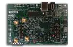


 工商网监
湘ICP备2023018690号
工商网监
湘ICP备2023018690号
