User's Guide
SLAU480C – January 2013 – Revised May 2014
AFE4400 and AFE4490 Development Guide
This user’s guide describes the characteristics, operation, and use of the AFE44x0SPO2EVM
demonstration kit. This demonstration kit is an evaluation module (EVM) for the AFE4400 and AFE4490
family of devices. The family of devices are fully-integrated AFE, ideally suited for pulse oximeter
applications. The EVM is intended for prototyping and evaluation. This user’s guide includes a complete
circuit description, schematic diagram, and bill of materials.
The following related documents are available through the Texas Instruments website at www.ti.com.
1
2
3
4
5
6
7
8
9
10
Device
Literature Number
AFE4400
SBAS601
AFE4490
SBAS602
Contents
AFE44x0SPO2EVM Overview ............................................................................................. 2
1.1
Important Disclaimer Information ................................................................................. 2
Overview ...................................................................................................................... 3
2.1
Introduction .......................................................................................................... 3
2.2
AFE44x0SPO2EVM Kit Contents................................................................................. 3
2.3
Features Supported in this Version .............................................................................. 3
Software Installation ......................................................................................................... 4
3.1
Minimum Requirements ............................................................................................ 4
3.2
Installing the Software (PC Application) ......................................................................... 5
3.3
Installing the USB Drivers ......................................................................................... 8
Running the Software ...................................................................................................... 15
4.1
Overview of the Features ........................................................................................ 15
AFE44x0SPO2EVM Hardware ........................................................................................... 27
5.1
Power Supply ...................................................................................................... 29
5.2
Clock ................................................................................................................ 29
5.3
Accessing AFE44x0 Digital Signals ............................................................................. 30
5.4
Analog Inputs ...................................................................................................... 30
5.5
USB Interface ...................................................................................................... 30
5.6
On-Board Key Interface .......................................................................................... 30
5.7
Visual Indication ................................................................................................... 31
USB-Based Firmware Upgrade .......................................................................................... 31
GUI Update ................................................................................................................. 33
Connector Interface ........................................................................................................ 34
8.1
DB9 Pulse Oximeter Connector ................................................................................. 34
8.2
Mini USB Connector .............................................................................................. 34
Quick Start Guide .......................................................................................................... 36
AFE44x0SPO2EVM FAQs ................................................................................................ 37
10.1 EVM Communicating With the PC Application ................................................................ 37
10.2 ADC_RDY Signal.................................................................................................. 37
10.3 Check TXP and TXM Waveforms ............................................................................... 38
10.4 Using an External ADC (Bypass ADC Mode) (Available Only for AFE4490 Device) .................... 39
10.5 Diagnostics ......................................................................................................... 39
10.6 Automation of Register Read and Write Operations.......................................................... 39
10.7 Optimum Viewing Experience on Windows 7 OS ............................................................. 40
SLAU480C – January 2013 – Revised May 2014
Submit Documentation Feedback
AFE4400 and AFE4490 Development Guide
Copyright © 2013–2014, Texas Instruments Incorporated
1
�AFE44x0SPO2EVM Overview
11
12
www.ti.com
10.8 Windows 8 Support for Device GUIs ...........................................................................
10.9 COM Port ...........................................................................................................
Bill of Materials .............................................................................................................
PCB Layouts and Schematics ............................................................................................
12.1 AFE44x0SPO2EVM PCB Layouts ..............................................................................
12.2 AFE44x0SPO2EVM Schematics ................................................................................
40
46
47
50
50
55
List of Tables
1
Save Tab Control Descriptions ........................................................................................... 27
2
Test Points for Measuring Voltages on the AFE4490SPO2EVM .................................................... 29
3
Test Points for Measuring Voltages on the AFE4400SPO2EVM .................................................... 29
4
AFE44x0 Digital Signals ................................................................................................... 30
5
AFE44x0SPO2EVM Switches ............................................................................................ 30
6
DB9-Based Pulse Oximeter Connector Pinouts ........................................................................ 34
7
USB Mini Connector Pinouts
8
9
.............................................................................................
Troubleshoot and Links ....................................................................................................
AFE44x0SPO2EVM Bill of Materials ....................................................................................
1
AFE44x0SPO2EVM Overview
1.1
Important Disclaimer Information
35
46
47
CAUTION
The AFE44x0SPO2EVM is intended for feasibility and evaluation testing only in
laboratory and development environments. This product is not for diagnostic
use. This product is not for use with a defibrillator.
Only use the AFE44x0SPO2EVM under the following conditions:
• The AFE44x0SPO2EVM demonstration kit is intended only for electrical evaluation of the features of
the AFE44x0 devices in a laboratory, simulation, or development environment.
• The AFE44x0SPO2EVM demonstration kit is not intended for direct interface with a patient, or patient
diagnostics.
• The AFE44x0SPO2EVM demonstration kit is intended for development purposes ONLY. It is not
intended to be used as all or part of an end-equipment application.
• The AFE44x0SPO2EVM demonstration kit should be used only by qualified engineers and technicians
who are familiar with the risks associated with handling electrical and mechanical components,
systems, and subsystems.
• The user is responsible for the safety of themself, fellow employees and contractors, and coworkers
when using or handling the AFE44x0SPO2EVM. Furthermore, the user is fully responsible for the
contact interface between the human body and electronics; consequently, the user is responsible for
preventing electrical hazards such as shock, electrostatic discharge, and electrical overstress of
electric circuit components.
Pentium, Celeron are registered trademarks of Intel Corporation.
Windows is a trademark of Microsoft Corporation.
Microsoft is a registered trademark of Microsoft Corporation.
National Instruments is a trademark of National Instruments Corporation.
2
AFE4400 and AFE4490 Development Guide
SLAU480C – January 2013 – Revised May 2014
Submit Documentation Feedback
Copyright © 2013–2014, Texas Instruments Incorporated
�Overview
www.ti.com
2
Overview
2.1
Introduction
NOTE: From this point on, unless otherwise noted, AFE44x0 refers to AFE4400- and AFE4490based demonstration kits.
The EVM is intended for evaluating AFE4400 and AFE4490 devices. The family of devices consist of a
low-noise receive channel, the LED transmit section, and diagnostics for sensor and LED fault detection.
The AFE44x0 has a highly configurable timing controller, enabling complete control of the device’s timing
characteristics. The device also has an integrated oscillator working off from two clock sources: either an
external crystal or the clock from an external host processor to ease clocking requirements and provide a
low-jitter clock to the AFE44x0. The device communicates to the external host processor using the serial
peripheral interface (SPI). The purpose of the EVM is to expedite evaluation and system development
activities related to AFE44x0 devices. The AFE4490SPO2EVM demonstration kit is shown in Figure 1.
Figure 1. AFE4490SPO2EVM Demonstration Kit
The board can be assembled with either of these devices. Check the TI website for the
AFE4400SPO2EVM and AFE4490SPO2EVM demonstration kits. The MSP430 firmware and PC
application are designed to automatically detect and configure to the installed part.
Throughout the document, the term demonstration kit is synonymous with AFE44x0SPO2EVM.
2.2
AFE44x0SPO2EVM Kit Contents
•
•
•
2.3
AFE44x0SPO2EVM Demonstration Kit
USB-to-mini USB cable
DB9 pulse oximeter cable
Features Supported in this Version
1. DB9 pulse oximeter sensor cable support
2. Acquire data at up to 3000 Hz in evaluation mode
3. USB-based power and PC application connectivity
SLAU480C – January 2013 – Revised May 2014
Submit Documentation Feedback
AFE4400 and AFE4490 Development Guide
Copyright © 2013–2014, Texas Instruments Incorporated
3
�Software Installation
www.ti.com
4. Access to all AFE44x0 registers through an easy-to-use GUI
5. Built-in time domain, histogram, FFT, and related analysis on the PC application
6. USB-based firmware upgrade option
3
Software Installation
The latest AFE44x0SPO2EVM PC application software (GUI) is available from the TI website,
AFE4400SPO2EVM GUI and AFE4490SPO2EVM GUI. Download the zipped file to a temporary directory
on the PC.
3.1
Minimum Requirements
Before installing the software, verify that your PC meets the minimum requirements outlined in this
section.
3.1.1
•
•
•
•
•
•
4
Required Setup for AFE44x0SPO2EVM Demo Software
IBM PC-compatible computer
Pentium® III/ Celeron® 866 MHz or equivalent processor
Minimum 256 MB of RAM (512 MB or greater recommended)
Hard disk drive with at least 200 MB free space
Microsoft® Windows™ XP SP2, Windows 7, or Windows 8 operating system
1280 × 1024 or greater display screen resolution
AFE4400 and AFE4490 Development Guide
SLAU480C – January 2013 – Revised May 2014
Submit Documentation Feedback
Copyright © 2013–2014, Texas Instruments Incorporated
�Software Installation
www.ti.com
3.2
Installing the Software (PC Application)
Before installing the software, make sure the AFE44x0SPO2EVM is NOT connected to the PC. If using a
machine with Windows 7 or Windows 8 OS, TI recommends having administrator rights to avoid problems
during installation. Unzip the installer file, and then find and double click setup.exe to install the software.
Unless otherwise specified during the install process, the software installs at the following location:
•
•
On a Windows XP machine
– C:\Program Files\Texas Instruments\AFE44x0SPO2EVM GUI
On a Windows 7 or Windows 8 machine
– C:\Program Files(x86)\Texas Instruments\AFE44x0SPO2EVM GUI
It creates a program menu item, AFE44x0SPO2EVM GUI under Programs→Texas
Instruments→AFE44x0SPO2EVM GUI to execute the software. The following steps ensure proper
installation of the PC application.
Click setup.exe and follow the prompts to continue with the installation process.
Select the destination directory and click the Next button.
Figure 2. PC Application Installation – Screen 1
SLAU480C – January 2013 – Revised May 2014
Submit Documentation Feedback
AFE4400 and AFE4490 Development Guide
Copyright © 2013–2014, Texas Instruments Incorporated
5
�Software Installation
www.ti.com
Accept the Texas Instruments end-user license agreement (EULA) and click the Next button.
Figure 3. PC Application Installation – Screen 2
Accept the National Instruments™ software license agreement and click the Next button.
Figure 4. PC Application Installation – Screen 3
6
AFE4400 and AFE4490 Development Guide
SLAU480C – January 2013 – Revised May 2014
Submit Documentation Feedback
Copyright © 2013–2014, Texas Instruments Incorporated
�Software Installation
www.ti.com
Click the Next button to begin the installation.
Figure 5. PC Application Installation – Screen 4
The application software is now installed. After the installation is complete, click the Next button to
continue with the installation of Python v2.7.
Figure 6. PC Application Installation – Screen 5
After the Python v2.7 is installed, click OK. The PC application is now ready to use.
Figure 7. Python Installation
SLAU480C – January 2013 – Revised May 2014
Submit Documentation Feedback
AFE4400 and AFE4490 Development Guide
Copyright © 2013–2014, Texas Instruments Incorporated
7
�Software Installation
3.3
www.ti.com
Installing the USB Drivers
The communication interface between the AFE44x0SPO2EVM board and PC is through the USB, using
the CDC profile. A one-time installation of the USB driver is required for the communication between the
AFE44x0SPO2EVM and PC application.
NOTE: For Windows 8, signed driver enforcement may have to be disabled. Section 3.3.1 explains
how to do this.
Following these steps ensures proper installation of the USB drivers:
1. Plugin the USB-to-mini USB cable to J4 of AFE44x0SPO2EVM and the other end to the USB port on
the PC.
2. Win XP OS starts up the New Hardware Wizard to enable the user to install the USB driver for the new
hardware. The Windows 7 or Windows 8 OS attempts to find the driver for the new hardware found
automatically and if the driver is not found, there is no pop-up message to indicate that the driver
installation failed. In the Windows 7 or Windows 8 OS, click on Device Manager, right click on
MSP430-USB example under Other devices and click on Update Driver Software as shown in
Figure 8. This step is not required for the Windows XP OS.
Figure 8. USB Driver Installation – Screen 1 (Win 7 OS only)
8
AFE4400 and AFE4490 Development Guide
SLAU480C – January 2013 – Revised May 2014
Submit Documentation Feedback
Copyright © 2013–2014, Texas Instruments Incorporated
�Software Installation
www.ti.com
3. Select the Install from a list or specific locations (Advanced) option, and click the Next button.
Figure 9. USB Driver Installation – Screen 2
4. As shown in Figure 10, navigate to the directory where the AFE44x0.inf file is located by clicking the
Browse button. The file is located at the following path:
• On a Windows XP machine:
– C:\Program Files\Texas Instruments\AFE44x0SPO2EVM GUI\USB Driver
• On a Windows 7 or Windows 8 machine:
– C:\Program Files(x86)\Texas Instruments\AFE44x0SPO2EVM GUI\USB Driver
Click the Next button to continue. The Driver file is copied to the system directory after clicking the
Next button.
Figure 10. USB Driver Installation – Screen 3
SLAU480C – January 2013 – Revised May 2014
Submit Documentation Feedback
AFE4400 and AFE4490 Development Guide
Copyright © 2013–2014, Texas Instruments Incorporated
9
�Software Installation
www.ti.com
5. Click the Finish button after the driver installation is complete (Figure 11).
Figure 11. USB Driver Installation – Screen 4
6. The AFE44x0SPO2-FE EVM is now recognized as Virtual COM Port under the Device Manager as
shown in Figure 12.
Figure 12. Device Manager Screen
The USB driver installation is now complete and the EVM is ready to use.
10
AFE4400 and AFE4490 Development Guide
SLAU480C – January 2013 – Revised May 2014
Submit Documentation Feedback
Copyright © 2013–2014, Texas Instruments Incorporated
�Software Installation
www.ti.com
3.3.1
Windows 8 Installing Unsigned Drivers
Perform an advanced startup sequence to let Windows 8 install unsigned drivers.
Move the cursor to the top right of the screen, click settings, then power, then HOLD SHIFT and click
Restart as shown in Figure 13.
Figure 13.
SLAU480C – January 2013 – Revised May 2014
Submit Documentation Feedback
AFE4400 and AFE4490 Development Guide
Copyright © 2013–2014, Texas Instruments Incorporated
11
�Software Installation
www.ti.com
After a loading screen, three options appear. Choose Troubleshoot as shown in Figure 14.
Figure 14.
Choose advanced options as shown in Figure 15.
Figure 15.
12
AFE4400 and AFE4490 Development Guide
SLAU480C – January 2013 – Revised May 2014
Submit Documentation Feedback
Copyright © 2013–2014, Texas Instruments Incorporated
�Software Installation
www.ti.com
Choose startup Settings as shown in Figure 16.
Figure 16.
Next a list of options displays. Click Restart at the bottom right as shown in Figure 17.
Figure 17.
SLAU480C – January 2013 – Revised May 2014
Submit Documentation Feedback
AFE4400 and AFE4490 Development Guide
Copyright © 2013–2014, Texas Instruments Incorporated
13
�Software Installation
www.ti.com
After the computer restarts, the following screen appears (see Figure 18). Press F7 to disable driver
signature enforcement.
Figure 18.
Now, the user can install unsigned drivers. A warning may appear as shown in Figure 19; choose Install
this driver software anyway.
Figure 19.
Restart the computer again to re-enable driver signature enforcement after the installation is complete.
14
AFE4400 and AFE4490 Development Guide
SLAU480C – January 2013 – Revised May 2014
Submit Documentation Feedback
Copyright © 2013–2014, Texas Instruments Incorporated
�Running the Software
www.ti.com
4
Running the Software
Run the GUI software from the Start menu by selecting
All Programs→Texas Instruments→AFE44x0SPO2EVM GUI. Unless the hardware has been
disconnected, observe messages that confirm the connection has been established and the program waits
in idle mode for user input.
If the connection to the AFE44x0SPO2EVM board is not established, the program prompts to continue to
run the GUI in Simulation mode, or to Stop and Close the GUI and check if the AFE44x0SPO2EVM is
connected to the PC.
Figure 20. AFE44x0SPO2EVM Not Connected Error Message
4.1
Overview of the Features
This section provides a quick overview of the various features and functions of the AFE44x0SPO2EVM
software GUI. The GUI allows the user to easily configure the various functions of the AFE, such as
receiver gain, bandwidth settings, LED current settings, and timing and clocking control settings. The GUI
supports both AFE4400 and AFE4490 devices. Features not available for the AFE4400 device are
disabled and are not shown in the AFE4400SPO2EVM GUI.
Operations in the GUI should only be performed after the status bar (located at the bottom of the GUI)
displays Ready For New Command (refer to Figure 21).
The main tabs consist of:
• About – Product Safety Warnings, Restrictions, and Disclaimers (see Figure 21).
• Device Configuration – Configures all the AFE44x0 user registers in a series of related subtabs.
– Global Settings
– Tx Stage
– Rx Stage
– Timing Controls
– Low Level Configuration
• ADC Capture & Analysis – For viewing and analyzing the raw data.
• Save – For writing data samples and analysis results to a file.
SLAU480C – January 2013 – Revised May 2014
Submit Documentation Feedback
AFE4400 and AFE4490 Development Guide
Copyright © 2013–2014, Texas Instruments Incorporated
15
�Running the Software
www.ti.com
Figure 21. Product Safety Warnings, Restrictions, and Disclaimers
4.1.1
Device Configuration Tab
The Device Configuration tab allows configuration of the various registers of the AFE44x0 device. This
subtab contains five subtabs: Global Settings, Tx Stage, Rx Stage, Timing Controls, and Low Level
Configuration.
4.1.1.1
Global Settings Subtab
The Global Settings subtab for the AFE4490 device shown in Figure 22 and for AFE4400 device shown in
Figure 23 has the following features:
1. View the Device ID and Firmware Revision
2. Device Reset button that resets the device. (Please note that after a device reset is issued, the
AFE44x0 device registers must be programmed correctly for the PC application GUI to function
properly. See Reset to EVM Defaults on how to issue a device reset and also program the AFE44x0
registers to the EVM default register settings.)
3. Reset to EVM Defaults button that resets the device and sets up the board to the EVM default
register settings.
4. Enables the user to set or reset:
(a) SPI Read
(b) XTAL Disable
(c) En Bypass ADC (available for AFE4490 device only)
(d) Powerdown AFE
(e) Powerdown TX
(f) Powerdown RX
(g) Enable Slow Diag Clock (available for AFE4490 device only)
(h) Enable CLKs on ALM Pin and select the following clocks to route to PD_ALM and LED_ALM pins
16
AFE4400 and AFE4490 Development Guide
SLAU480C – January 2013 – Revised May 2014
Submit Documentation Feedback
Copyright © 2013–2014, Texas Instruments Incorporated
�Running the Software
www.ti.com
(i) Sample LED2 and LED1 pulse
(ii) LED2 / LED1 LED pulse
(iii) Sample LED2 / LED1 Ambient pulse
(iv) LED2 / LED1 Convert pulse
(v) LED2 / LED1 Ambient Convert pulse
5. Click on Diagnostic Enable and view the Alarm status flags triggered through Diagnostic Enable.
Figure 22. AFE4490: Device Configuration: Global Settings
SLAU480C – January 2013 – Revised May 2014
Submit Documentation Feedback
AFE4400 and AFE4490 Development Guide
Copyright © 2013–2014, Texas Instruments Incorporated
17
�Running the Software
www.ti.com
Figure 23. AFE4400: Device Configuration: Global Settings
18
AFE4400 and AFE4490 Development Guide
SLAU480C – January 2013 – Revised May 2014
Submit Documentation Feedback
Copyright © 2013–2014, Texas Instruments Incorporated
�Running the Software
www.ti.com
4.1.1.2
Tx Stage Subtab
The Tx Stage subtab under the Device Configuration tab, shown in Figure 24 for AFE4490 and Figure 25
for AFE4400, consists of the settings to:
1. Set LED1 and LED2 currents.
2. Program LED current control DAC through a pull-down menu.
3. Program the transmitter reference voltage through a pull-down menu (available for AFE4490 device
only).
4. Select between H-bridge mode and Push-pull mode.
NOTE: The AFE44x0SPO2EVM does not support Push-pull mode.
4.1.1.3
Rx Stage Subtab
The Rx Stage subtab under the Device Configuration tab, shown in Figure 26 for AFE4490 and Figure 27
for AFE4400, consists of the settings to:
1. Enable separate gain mode (available for AFE4490 device only).
2. Set feedback resistance and capacitance for the trans-impedance amplifier with separate gain mode
disabled.
3. Set feedback resistance and capacitance for the trans-impedance amplifier with separate gain mode
enabled (available for AFE4490 device only).
4. Enable second-stage and set gain for the second-stage amplifier.
5. Set ambient DAC current.
6. Select filter corner frequency (available for AFE4490 device only).
Figure 24. AFE4490: Device Configuration: Tx Stage
SLAU480C – January 2013 – Revised May 2014
Submit Documentation Feedback
AFE4400 and AFE4490 Development Guide
Copyright © 2013–2014, Texas Instruments Incorporated
19
�Running the Software
www.ti.com
Figure 25. AFE4400: Device Configuration: Tx Stage
Figure 26. AFE4490: Device Configuration: Rx Stage
20
AFE4400 and AFE4490 Development Guide
SLAU480C – January 2013 – Revised May 2014
Submit Documentation Feedback
Copyright © 2013–2014, Texas Instruments Incorporated
�Running the Software
www.ti.com
Figure 27. AFE4400: Device Configuration: Rx Stage
4.1.1.4
Timing Controls Subtab
The Timing Controls subtab under the Device Configuration tab, shown in Figure 28 for AFE4490 and
Figure 29 for AFE4400, consists of the following settings:
1. Enter the Pulse Repetition Frequency (PRF) and Duty Cycle % and click the SET button to
automatically set the following:
(a) LED1 (IR) and LED2 (Red) ON and OFF time,
(b) Rx sample start and end time for 4 channels (LED1, LED1 Ambient, LED2, LED2 Ambient)
(c) Rx convert start and end time for 4 channels (LED1, LED1 Ambient, LED2, LED2 Ambient)
2. Save the timing settings based on PRF and duty cycle to a configuration file
3. Load the timing settings based on PRF and duty cycle from a configuration file
4. Timer Enable selector
5. Timer Counter RESET button
6. Set Number of Averages (available for AFE4490 device only)
SLAU480C – January 2013 – Revised May 2014
Submit Documentation Feedback
AFE4400 and AFE4490 Development Guide
Copyright © 2013–2014, Texas Instruments Incorporated
21
�Running the Software
www.ti.com
Figure 28. AFE4490: Device Configuration: Timing Controls
Figure 29. AFE4400: Device Configuration: Timing Controls
22
AFE4400 and AFE4490 Development Guide
SLAU480C – January 2013 – Revised May 2014
Submit Documentation Feedback
Copyright © 2013–2014, Texas Instruments Incorporated
�Running the Software
www.ti.com
4.1.1.5
Low Level Configuration Subtab
The Low Level Configuration subtab under the Device Configuration tab is used to directly configure the
various registers of the AFE44x0 devices. Refer to the AFE44x0 data sheet (SBAS601, SBAS602) for the
register details of the chip.
Figure 30 shows the low-level configuration registers of the AFE44x0 devices. The Register Map portion
of the sub-tab shows the EVM default values of the registers after the GUI is loaded under the EVM
Default column. The LW* column shows the latest written values of the AFE44x0 register and the LR*
column shows the latest read values of the AFE44x0 registers. From the Register Map section, when any
register is selected, the bit-level details about the register are explained in the Register Description
section. The ability to read and write the register and modify the individual bits of the register are provided
in the Register Data section. The values of all the registers are read by clicking the Read All button.
Click on Transfer Read to Write to copy the contents of the Read Data to Write Data. Then click on Write
Register to write to the data to the register of the AFE44x0.
By clicking on the Save Config button, the register configuration is saved to a configuration file. The
register configuration is loaded from a configuration file by clicking the Load Config button.
Figure 30. Device Configuration: Low Level Configuration
When a selection is made on any of the tabs on the GUI, multiple fields of various registers are modified.
Click on the lower-left corner of the GUI to view the registers that are modified when a selection is made.
4.1.2
ADC Capture and Analysis
The ADC Capture and Analysis tab consists of various analysis routines and displays. This tab is used to:
• Set the capture mode to finite or continuous
• Set the number of samples (block size) in Finite Capture mode
• Set the display to volts or codes
• Set the filter type to None or Notch
• Set the Notch Freq to 50 or 60 Hz when the filter type is set to Notch
SLAU480C – January 2013 – Revised May 2014
Submit Documentation Feedback
AFE4400 and AFE4490 Development Guide
Copyright © 2013–2014, Texas Instruments Incorporated
23
�Running the Software
•
•
•
www.ti.com
Set Analysis Type to All Domain or Time Domain only
Auto save after capture selector
Acquire the data by clicking the Capture button
– When the user selects the auto save after capture selector under 'ADC Capture & Analysis' tab, the
GUI uses the settings selected under 'Analysis to Save,' 'Channels to Save,' 'Data to Save,' and
'Save File Settings'. The user will be notified with a 'Results saved successfully!' after every
capture.
The captured data can be analyzed in time domain and frequency domain; the data can also be displayed
in a histogram format. The ADC Capture and Analysis tab is shown in Figure 31.
By selecting the Time Domain plot, the data are displayed in time domain format. The units can be
converted from codes to volts using the drop-down window in the top-left corner of the GUI. For the time
domain plot, the mean voltage, root mean square (RMS) voltage, and peak-to-peak voltage are displayed
in the Test Results section, which is a pop-up window that opens when the Scope Analysis button is
clicked. The Scope Analysis: Test Results section pop-up window is shown in Figure 32.
By selecting the FFT plot, the data are displayed in the frequency domain by performing an FFT on the
channel selected. Details of the FFT (including SNR, THD, and so on) are shown in the Test Results
section located in the left side of the GUI.
Selecting the Histogram plot displays the data in a histogram format for the channel selected. The data
are arranged in the total number of histogram bins set within the tab following acquisition. The histogram
analysis (shown in the Test Results section of the GUI) is used to view the mean voltage, root mean
square (RMS) voltage, and peak-to-peak voltage.
Four plot modes can be selected: Single Plot mode, Double Plot mode, Three Plot mode and Four Plot
mode. In Single Plot mode, only one plot (Time, FFT, or Histogram) can be viewed and analyzed for post
processing. In Double Plot mode, any two plots (Time, FFT or Histogram) can be viewed and analyzed. In
Three Plot mode, any three plots and in Four Plot mode, any four plots (Time, FFT or Histogram) can be
viewed and analyzed.
The following algorithms have been used to find the # of samples for FFT calculation:
(a) # of samples for FFT calc. which is power of 2 ≤ min ( (Data rate (sps) × N where N is the value in the
"Show data for the last N secs" column) , No. of samples )
(b) If ( (# of samples for FFT calc. == No. of samples) && (Filter Type == “None”) ) then # of samples for
FFT calc. = No. of samples
(c) If ( (# of samples for FFT calc. == No. of samples) && (Filter Type == “Notch”) ) then # of samples for
FFT calc. = No. of samples / 2. This is to allow for filter settling.
(d) If ( # of samples for FFT calc. < 32 samples ) then an error msg “Insufficient # of samples for FFT
calculation” will be displayed.
Examples:
1. No. of samples = 8192
Data rate (sps) = 500
Show data for the last 5 secs
Then # of samples for FFT calc. which is power of 2 = 2048 ≤ min ( (500 × 5) , 8192 )
2. No. of samples = 8192
Data rate (sps) = 500
Show data for the last 8 secs
Then # of samples for FFT calc. which is power of 2 = 2048 ≤ min ( (500 x 8) , 8192 )
3. No. of samples = 8192
Data rate (sps) = 500
Show data for the last 20 secs
# of samples for FFT which is power of 2 = 8192 ≤ min ( (500 x 20) , 8192 )
Since (# of samples for FFT calc. == No. of samples) and if (Filter Type = None) then # of
samples for FFT which is power of 2 = 8192
Since (# of samples for FFT calc. == No. of samples) and if (Filter Type = Notch) then # of
samples for FFT which is power of 2 = 8192 / 2
24
AFE4400 and AFE4490 Development Guide
SLAU480C – January 2013 – Revised May 2014
Submit Documentation Feedback
Copyright © 2013–2014, Texas Instruments Incorporated
�Running the Software
www.ti.com
4. No. of samples = 30
Data rate (sps) = 500
Show data for the last 1 secs
Then display Error message “Insufficient # of samples for FFT calculation” since # of samples
for FFT which is power of 2 = 16 ≤ min ( (500 x 1) , 30 )
5. No. of samples = 32
Data rate (sps) = 500
Show data for the last 2 secs
# of samples for FFT which is power of 2 = 32 ≤ min ( (500 x 2) , 32 )
Since (# of samples for FFT calc. == No. of samples) and If (Filter Type = None) then # of
samples for FFT calc. which is power of 2 = 32
Since (# of samples for FFT calc. == No. of samples) and If (Filter Type = Notch) then an error
msg “Insufficient # of samples for FFT calculation” will be displayed since # of samples for FFT
calc. which is power of 2 = (32 / 2) < 32 samples
Figure 31. ADC Capture and Analysis Tab
Figure 32. Scope Analysis: Test Results
SLAU480C – January 2013 – Revised May 2014
Submit Documentation Feedback
AFE4400 and AFE4490 Development Guide
Copyright © 2013–2014, Texas Instruments Incorporated
25
�Running the Software
4.1.3
www.ti.com
Save Tab
The Save tab shown in Figure 33 provides provisions to save the analysis or data to a file. By default, the
data are saved to the following location:
•
•
On a Windows XP machine
– C:\Program Files\Texas Instruments\AFE44x0SPO2EVM GUI\Log
On a Windows 7 or Windows 8 machine
– C:\Program Files(x86)\Texas Instruments\AFE44x0SPO2EVM GUI\Log
Use the Directory to Save Files option to select the folder where data are to be saved. In the pop-up
window, navigate to the folder where the data file is to be saved and select Use Current Folder. Then
select Save to File to save the file.
When the user selects the auto save after capture selector under 'ADC Capture & Analysis' tab, the GUI
uses the settings selected under 'Analysis to Save,' 'Channels to Save,' 'Data to Save,' and 'Save File
Settings'. The user will be notified with a 'Results saved successfully!' after every capture.
Figure 33. Save Tab
26
AFE4400 and AFE4490 Development Guide
SLAU480C – January 2013 – Revised May 2014
Submit Documentation Feedback
Copyright © 2013–2014, Texas Instruments Incorporated
�AFE44x0SPO2EVM Hardware
www.ti.com
Table 1 contains the Save tab control descriptions.
Table 1. Save Tab Control Descriptions
Button/Control
Description
Scope Analysis
Saves the scope analysis result.
The result is saved in the file Device__Analysis.xls.
FFT Analysis
Saves the FFT analysis result.
The result is saved in the file Device__Analysis.xls.
Histogram Analysis
Saves the histogram analysis result.
The result is saved in the file Device__Analysis.xls.
Register Settings
All the current register values are read from the EVM and stored.
The result is saved in the file Device__Analysis.xls.
Data – Codes
Acquired data sample values are stored to the file Device_ _Codes.xls.
FFT Data
Acquired data sample’s FFT values are stored to the file Device_ _FFT.xls.
Histogram Data
Acquired data sample’s histogram values are stored to the file Device_ _Histogram.xls.
The Record Number saves files with the provided number in the file name. User notes can also be added
to the file by typing the notes in the User Comments control.
5
AFE44x0SPO2EVM Hardware
CAUTION
Many of the components on the AFE44x0SPO2EVM are susceptible to damage
by electrostatic discharge (ESD). Customers are advised to observe proper
ESD handling precautions when unpacking and handling the EVM, including
the use of a grounded wrist strap, bootstraps, or mats at an approved ESD
workstation. Safety glasses should also be worn.
The key features of the AFE44x0 Analog Front End demonstration board are:
• Based on MSP430F5529
• DB9 pulse oximeter sensor cable support
• Acquire data at up to 3000 Hz in evaluation mode
• SPI Data interface
The AFE44x0SPO2EVM board can be used as a demo board for pulse oximeter and heart rate
applications. The BOM is provided in Section 11. The printed circuit board (PCB) and schematic are
shown in Section 12.1 and Section 12.2, respectively.
MSP430F5529 (U2 – see Section 12.2) is the microcontroller used on the board. For more details of the
MSP430F5529 please visit http://focus.ti.com/docs/prod/folders/print/msp430f5529.html
The following sections explain the main hardware components available on the EVM. Figure 34 shows the
functional block diagram for the EVM.
SLAU480C – January 2013 – Revised May 2014
Submit Documentation Feedback
AFE4400 and AFE4490 Development Guide
Copyright © 2013–2014, Texas Instruments Incorporated
27
�AFE44x0SPO2EVM Hardware
www.ti.com
6pin eZ430
RF header
UART
SD CARD
AFE4490
SPI
MSP430F5529
SPI
2Mb
FRAM
2Mb
FRAM
Memory Block
MSP Reset
Switch
DB9
Connector
Accelerometer
MSP
JTAG
Header
USB Reset
Switch
I2C
AFE4490
Evaluation
Module
AFE RX
3V LDO
AFE TX
5V LDO
MSP430
3V LDO
Batt
FuelGauge
Boost
Converter
Battery
Mgmt
Mini
USB
Battery
Header
Power Management Block
a. AFE4490 Evaluation Module
6pin eZ430
RF header
UART
SD CARD
AFE4400
SPI
MSP430F5529
SPI
2Mb
FRAM
2Mb
FRAM
Memory Block
MSP Reset
Switch
DB9
Connector
Accelerometer
USB Reset
Switch
I2C
AFE4400
Evaluation
Module
AFE RX
3V LDO
AFE TX
3.3V LDO
MSP430
3V LDO
Batt
FuelGauge
Boost
Converter
Battery
Mgmt
MSP
JTAG
Header
Mini
USB
Battery
Header
Power Management Block
b. AFE4400 Evaluation Module
Figure 34. AFE44x0SPO2EVM Block Diagram
28
AFE4400 and AFE4490 Development Guide
SLAU480C – January 2013 – Revised May 2014
Submit Documentation Feedback
Copyright © 2013–2014, Texas Instruments Incorporated
�AFE44x0SPO2EVM Hardware
www.ti.com
5.1
Power Supply
AFE4490 can operate from 2.0- to 3.6-V Rx analog supply (RX_ANA_SUP), 2.0- to 3.6-V Rx digital supply
(RX_DIG_SUP), 3.0- to 5.25-V Tx Control supply (TX_CTRL_SUP) and LED driver supply
(LED_DRV_SUP).
AFE4400 can operate from 2.0- to 3.6-V Rx analog supply (RX_ANA_SUP), 2.0- to 3.6-V Rx digital supply
(RX_DIG_SUP), 3.0- to 3.6-V Tx Control supply (TX_CTRL_SUP) and LED driver supply
(LED_DRV_SUP).
The power for the board is derived from the USB input (J4) through a forward-biased diode (D5) to avoid
reverse current flow. The USB data bus is ESD protected using TI’s ESD protection diode array
TPD4E004DRYR (U7). The USB VBUS is fed to the integrated Li-ion linear charger and system powerpath management module, BQ24032ARHLR (U12), which generates greater than 4.2-V output
(VCC_BAT). This output is fed to TI’s low-input boost converter with integrated power diode and
input/output isolation, TPS61093 (U9), for generating a boosted voltage of 8.97 V. This output is fed to
low-noise voltage regulator LP3878-ADJ (U8) for generating 5 V for the LED_DRV_SUP and
TX_CTRL_SUP for AFE4490 EVM and for generating 3.3 V for the LED_DRV_SUP and TX_CTRL_SUP
for AFE4400 EVM. The boost converter output is also fed to the ultralow-noise linear voltage regulator
TPS7A4901DGN (U13) for generating 3 V for the RX_ANA_SUP and RX_DIG_SUP. The boost converter
output is also fed to the ultralow-noise linear voltage regulator TPS7A4901DGN (U14) for generating 3 V
for MSP_DVCC and MSP_AVCC.
The inductors L2, L2, L4, and L5 are used to minimize the power supply noise induced by the power
supply regulators.
Test point and series jumper resistors are provided to make sure the power supplies to the board are
correct. The corresponding voltages on AFE4490SPO2EVM are given in Table 2. The corresponding
voltages on AFE4400SPO2EVM are shown in Table 3.
Table 2. Test Points for Measuring Voltages on the AFE4490SPO2EVM
S. No.
Test Point
Description
1
TP36
5V
2
L6, pin # 2 (R76)
5V
3
L5, pin # 2 (R65)
5V
4
L1, pin # 2 (R55)
3V
5
L2, pin # 2 (R54)
3V
6
L3, pin # 2
3V
Table 3. Test Points for Measuring Voltages on the AFE4400SPO2EVM
S. No.
5.2
Test Point
Description
1
TP36
5V
2
L6, pin # 2 (R76)
3.3 V
3
L5, pin # 2 (R65)
3.3 V
4
L1, pin # 2 (R55)
3V
5
L2, pin # 2 (R54)
3V
6
L3, pin # 2
3V
Clock
The EVM has the option to use the on-board 8-MHz crystal or the clock for the AFE44x0 from the
MSP430. The EVM is shipped to use the on-board 8-MHz crystal. The 4-MHz buffered output clock from
the AFE44x0 can be accessed through the series jumper resistor, R23.
SLAU480C – January 2013 – Revised May 2014
Submit Documentation Feedback
AFE4400 and AFE4490 Development Guide
Copyright © 2013–2014, Texas Instruments Incorporated
29
�AFE44x0SPO2EVM Hardware
5.3
www.ti.com
Accessing AFE44x0 Digital Signals
AFE44x0 SPI interface and other digital signals with MSP430 can be accessed through the series resistor
jumpers given in Table 4.
Table 4. AFE44x0 Digital Signals
5.4
S. No.
Signal
Jumper Resistor
1
STE
R29
2
SIMO
R31
3
SOMI
R33
4
SCLK
R35
5
ADC_RDY
R26
6
PD_ALM
R37
7
LED_ALM
R39
8
DIAG_END
R38
9
AFE_PDNZ
R42
Analog Inputs
The AFE44x0SPO2EVM gives the user the option to feed in the pulse oximeter simulator signals to the
DB9 connector (J2).
For all measurements in this user guide, the ProSim Fluke SPOT Light SpO2 Functional tester was used
as shown in Figure 35.
Figure 35. Fluke SPOT Light SpO2 Functional Tester Setup
5.5
USB Interface
The EVM has a mini USB interface for PC application connectivity requiring a standard mini USB to USB
cable for connection. AFE44x0SPO2EVM is designed to work in the slave mode.
5.6
On-Board Key Interface
The EVM has 2 switches. The function of each switch is defined in Table 5
Table 5. AFE44x0SPO2EVM Switches
30
Switch Number
Description
SW1
This switch is used for hard reset of the board. The board resets and starts again with the firmware loaded.
SW2
This switch is used to enable boot strap loader (BSL) MSP430 firmware.
AFE4400 and AFE4490 Development Guide
SLAU480C – January 2013 – Revised May 2014
Submit Documentation Feedback
Copyright © 2013–2014, Texas Instruments Incorporated
�AFE44x0SPO2EVM Hardware
www.ti.com
5.7
Visual Indication
The blue LED (LED3) indicates the USB power connection. The blue LED (LED1) indicates that the
microcontroller is busy servicing the requests from the PC application.
6
USB-Based Firmware Upgrade
NOTE: AFE44x0SPO2EVM GUI v2.0 works with FW rev 1.3. Follow the steps outlined in this
section to upgrade the firmware to rev 1.3.
The firmware on the AFE44x0SPO2EVM can be changed from the PC application by selecting the
Firmware Upgrade menu option on the PC application. At the end of the firmware upgrade, the system
issues a reset command and reloads with new firmware. The firmware upgrade process steps are
represented in the screen shots below:
• From the PC application, click on File →Firmware Upgrade.
• A pop-up window opens up as shown in Figure 36. Follow the instructions to continue to Firmware
Upgrade or to cancel the operation.
Figure 36. PC Application Firmware Upgrade – 1
•
The firmware upgrade application detects the connected EVM (Figure 37).
Figure 37. PC Application Firmware Upgrade – 2
•
Visually inspect the EVM and find out the device installed on the EVM. The EVM supports two devices
AFE4400 and AFE4490. Browse and select the appropriate firmware binary file (example:
AFE4490_EVM_FW_V1.3.txt file) and click Upgrade Firmware as shown in Figure 38. The default
firmware is available from:
SLAU480C – January 2013 – Revised May 2014
Submit Documentation Feedback
AFE4400 and AFE4490 Development Guide
Copyright © 2013–2014, Texas Instruments Incorporated
31
�USB-Based Firmware Upgrade
www.ti.com
– On a Windows XP machine:
• C:\Program Files\Texas Instruments\AFE44x0SPO2EVM GUI\Firmware Updater
– On a Windows 7 or Windows 8 machine:
• C:\Program Files(x86)\Texas Instruments\AFE44x0SPO2EVM GUI\Firmware Updater
Figure 38. PC Application Firmware Upgrade – 3
•
Once the device is programmed successfully, as shown in Figure 39, the device resets and reloads
with the new firmware. Close the Firmware Upgrade application by clicking on the Close button and
the PC GUI application automatically restarts the GUI after 4 to 5 seconds.
Figure 39. PC Application Firmware Upgrade – 4
32
AFE4400 and AFE4490 Development Guide
SLAU480C – January 2013 – Revised May 2014
Submit Documentation Feedback
Copyright © 2013–2014, Texas Instruments Incorporated
�GUI Update
www.ti.com
7
GUI Update
The user can check for the latest version of the GUI by selecting 'Check for New GUI Version' from the
menu options on the PC application as shown in Figure 40.
Figure 40. Check for New GUI Version
When a newer version of the GUI is available, a pop-up message will appear letting the user to download
the update now or at a later time. The latest version of the GUI will be downloaded to the following
directory:
• On a Windows XP machine:
– C:\Program Files\Texas Instruments\AFE44x0SPO2EVM GUI
• On a Windows 7 or Windows 8 machine:
– C:\Program Files(x86)\Texas Instruments\AFE44x0SPO2EVM GUI
If a newer version is not available, a pop-up message will let the user know that the current version is the
latest version of the GUI as shown in Figure 41.
Figure 41. Current GUI Version is the Latest Version
SLAU480C – January 2013 – Revised May 2014
Submit Documentation Feedback
AFE4400 and AFE4490 Development Guide
Copyright © 2013–2014, Texas Instruments Incorporated
33
�Connector Interface
8
www.ti.com
Connector Interface
The following connectors are used for external interface to the AFE44x0 Pulse Oximeter board.
• DB9
• USB mini connector
8.1
DB9 Pulse Oximeter Connector
The DB9 pulse oximeter connector pinouts are shown in Figure 42. The description of the pinouts is
provided in Table 6
Figure 42. DB9 Pulse Oximeter Connector Pinouts
Table 6. DB9-Based Pulse Oximeter Connector Pinouts
8.2
Pin Number
Pin Name
Pin Description
2
TX_LED_P
Anode of the LED1 (IR LED), cathode of the LED2 (red LED)
3
TX_LED_N
Cathode of the LED1 (IR LED), anode of the LED2 (red LED)
5
DET_N
Phototransistor anode
7
GND
Cable shield
9
DET_P
Phototransistor cathode
Mini USB Connector
The USB mini connector pinouts are shown in Figure 43. The description of the pinouts is provided in
Table 7.
Figure 43. USB Mini Connector Pinouts
34
AFE4400 and AFE4490 Development Guide
SLAU480C – January 2013 – Revised May 2014
Submit Documentation Feedback
Copyright © 2013–2014, Texas Instruments Incorporated
�Connector Interface
www.ti.com
Table 7. USB Mini Connector Pinouts
Pin Number
Pin Name
Pin Description
1
VBUS
USB power 5 V
2
D–
USB DM
3
D+
USB DP
4
ID
NC
5
GND
GND
SLAU480C – January 2013 – Revised May 2014
Submit Documentation Feedback
AFE4400 and AFE4490 Development Guide
Copyright © 2013–2014, Texas Instruments Incorporated
35
�Quick Start Guide
9
www.ti.com
Quick Start Guide
NOTE: For all the measurements shown in the following, ProSim Fluke SPOT Light SpO2
Functional tester was used.
•
•
•
•
•
•
•
Install the AFE44x0SPO2EVM GUI PC Software (Check the TI website at www.ti.com for the latest
software) by running the setup file and following the instructions on the screen
Connect the USB cable to the computer and plug in the mini USB interface cable to the J4 mini USB
connector on the EVM
Connect the DB9 connector of the finger sensor pulse oximeter cable to the J2 connector of the EVM.
Turn on the Fluke simulator by pressing the ON switch for at least 3 seconds, and then connect the
Fluke simulator to the finger sensor. Leave the default setting of 97% for SpO2, 80 bpm for HR, and
2% for PA. Figure 35 shows the Fluke SPOT Light Pulse SpO2 Functional Tester setup with the finger
sensor pulse oximeter cable.
Open the AFE44x0SPO2EVM GUI software by clicking on Start→All Programs→Texas
Instruments→AFE44x0SPO2EVM GUI.
Click the ADC Capture & Analysis tab and set the following:
– Capture Mode to Finite
– No. of Samples to 2048
– Volts/Codes to Volts
– Plot Mode to Four Plot Mode
– Select the first waveform to LED1 (IR)
– Select the second waveform to LED1 (IR) AMBIENT
– Select the third waveform to LED2 (Red)
– Select the fourth waveform to LED2 (Red) AMBIENT
– Click Capture
Figure 44 shows a sample data capture
Figure 44. Sample Test Data
36
AFE4400 and AFE4490 Development Guide
SLAU480C – January 2013 – Revised May 2014
Submit Documentation Feedback
Copyright © 2013–2014, Texas Instruments Incorporated
�AFE44x0SPO2EVM FAQs
www.ti.com
10
AFE44x0SPO2EVM FAQs
10.1 EVM Communicating With the PC Application
CAUTION
AFE44x0SPO2EVM GUI v.2.0 works with FW revision 1.3. Follow the steps
outlined in Section 6 to upgrade the firmware to revision 1.3.
A quick and simple check to verify serial register write operation is to put the AFE44x0 in power-down
mode. Follow the sequence to check if the GUI is communicating with the EVM.
• In Device Configuration→Global Settings tab, select Powerdown_AFE
• This powers down the AFE and the VCM output voltage of the AFE drops to 0 V
• VCM is measured at the VCM_AFE serial jumper resistor R28 on the board
10.2 ADC_RDY Signal
After executing the GUI, observe the ADC_RDY waveform at series jumper resistor R26.This should be at
the same frequency as the PRF. Figure 45 shows the ADC_RDY waveform at 500-Hz PRF.
Figure 45. ADC_RDY Waveform at 500-Hz PRF
SLAU480C – January 2013 – Revised May 2014
Submit Documentation Feedback
AFE4400 and AFE4490 Development Guide
Copyright © 2013–2014, Texas Instruments Incorporated
37
�AFE44x0SPO2EVM FAQs
www.ti.com
10.3 Check TXP and TXM Waveforms
TXP and TXM waveforms are observed at TX_P (TP23) and TX_N (TP17). Figure 46 shows TXP and
TXM waveforms without connecting the pulse oximeter cable. Figure 47 shows TXP and TXM waveforms
after connecting the pulse oximeter cable.
Figure 46. TXP and TXM Without Pulse Oximeter Cable
Figure 47. TXP and TXM After Connecting the Pulse Oximeter Cable
38
AFE4400 and AFE4490 Development Guide
SLAU480C – January 2013 – Revised May 2014
Submit Documentation Feedback
Copyright © 2013–2014, Texas Instruments Incorporated
�AFE44x0SPO2EVM FAQs
www.ti.com
10.4 Using an External ADC (Bypass ADC Mode) (Available Only for AFE4490 Device)
AFE4490 has a mode where the front-end analog output voltage becomes available on two pins
(RX_OUTP, RX_OUTN), around a common-mode voltage of about 0.9 V. In this mode, the internal ADC
of AFE4490 is disabled, one of the internal ADC_RESET clocks is brought out on the PD_ALM pin
(PD_ALM is monitored at series jumper resistor R37). This signal is used to convert each of the four
phases (with every pulse repetition period). Additionally the ADC_RDY signal (ADC_RDY is monitored at
series jumper resistor R26) is used to synchronize the external ADC with the AFE.
10.5 Diagnostics
The device includes diagnostics to detect open or short conditions of the LED and photo-sensor, LED
current profile feedback, and cable on or off detection. The EVM supports the diagnostic feature of the
device.
The diagnostic feature is enabled from the Global Settings under the Device Configuration tab. Clicking
the Diagnostic Enable button enables the diagnostic function and once the diagnostic function is
completed, the status of the fault flags are updated on the Global Settings tab. Figure 48 shows the
diagnostic mode fault flags when no finger pulse oximeter sensor was connected to the EVM.
Figure 48. Diagnostic Feature Fault Flags With No Finger Sensor Connected to the EVM
10.6 Automation of Register Read and Write Operations
Refer to the Scripting document located in the Documentation directory for detailed instruction on how to
use automation functions for register read and write operations.
Documentation directory is located at the following location:
• On a Windows XP machine – C:\Program Files\Texas Instruments\AFE44x0SPO2EVM
GUI\Documentation
• On a Windows 7 or Windows 8 machine – C:\Program Files(x86)\Texas
Instruments\AFE44x0SPO2EVM GUI\Documentation
SLAU480C – January 2013 – Revised May 2014
Submit Documentation Feedback
AFE4400 and AFE4490 Development Guide
Copyright © 2013–2014, Texas Instruments Incorporated
39
�AFE44x0SPO2EVM FAQs
www.ti.com
10.7 Optimum Viewing Experience on Windows 7 OS
•
Change the size of text to Smaller – 100% for optimum viewing experience on Windows 7 operating
system as shown in Figure 49.
Figure 49. Setting Font Size on Windows 7 Operating System
10.8 Windows 8 Support for Device GUIs
At GUI Start up, sometimes the GUI might show a broken arrow as seen in Figure 50. One of the reasons
for this issue may be due to a missing update of .NET FRAMEWORK 3.5 (includes .NET 2.0 and .NET
3.0).
Figure 50.
The .NET FRAMWORK 3.5 is needed for the GUI to:
• Check if Python is Installed
• Checking and setting environment variables needed for the scripting feature in the GUI
40
AFE4400 and AFE4490 Development Guide
SLAU480C – January 2013 – Revised May 2014
Submit Documentation Feedback
Copyright © 2013–2014, Texas Instruments Incorporated
�AFE44x0SPO2EVM FAQs
www.ti.com
Points to Remember:
• There is no download for the .NET Framework 3.5 for Windows 8 or Windows 8.1. The user must
enable the .NET Framework 3.5 in Control Panel by following the instructions provided in this article.
• Use the .NET Framework 3.5 for apps built for versions 2.0 and 3.0 as well as 3.5.
• Installing a Windows language pack before installing the .NET Framework 3.5 will cause the .NET
Framework 3.5 installation to fail. Install the .NET Framework 3.5 before installing any Windows
language packs. (Source: http://msdn.microsoft.com/library/hh506443(v=VS.110).aspx)
There are two methods to resolve this.
10.8.1
Method 1 (Enabling the .NET Framework 3.5 in Control Panel)
In Control Panel, choose Programs and Features, choose Turn Windows features on or off, and then
select the .NET Framework 3.5 (includes .NET 2.0 and 3.0) check box. This option requires an Internet
connection. The user does not need to select the child items.
Figure 51.
SLAU480C – January 2013 – Revised May 2014
Submit Documentation Feedback
AFE4400 and AFE4490 Development Guide
Copyright © 2013–2014, Texas Instruments Incorporated
41
�AFE44x0SPO2EVM FAQs
www.ti.com
Figure 52.
Select Download and Install this feature.
Figure 53.
42
AFE4400 and AFE4490 Development Guide
SLAU480C – January 2013 – Revised May 2014
Submit Documentation Feedback
Copyright © 2013–2014, Texas Instruments Incorporated
�AFE44x0SPO2EVM FAQs
www.ti.com
Select Download Files from Windows Update.
Figure 54.
Figure 55.
SLAU480C – January 2013 – Revised May 2014
Submit Documentation Feedback
AFE4400 and AFE4490 Development Guide
Copyright © 2013–2014, Texas Instruments Incorporated
43
�AFE44x0SPO2EVM FAQs
www.ti.com
Figure 56.
10.8.2
Method 2 (Enabling .NET Framework 3.5 on Windows 8 in Offline Mode)
This is basically using Windows 8 CD to enable/install .NET FRAMEWORK 3.5 in the PC. This method
does not require an internet connection.
Step 1: Insert Windows 8 DVD or mount ISO image. The source of this feature can be found in folder
E:\sources\sxs. (In this case E: is the user’s drive letter on which the user has loaded Windows 8 Media.)
Figure 57.
44
AFE4400 and AFE4490 Development Guide
SLAU480C – January 2013 – Revised May 2014
Submit Documentation Feedback
Copyright © 2013–2014, Texas Instruments Incorporated
�AFE44x0SPO2EVM FAQs
www.ti.com
Step 2: Open Command prompt as administrator.
Figure 58.
Figure 59.
SLAU480C – January 2013 – Revised May 2014
Submit Documentation Feedback
AFE4400 and AFE4490 Development Guide
Copyright © 2013–2014, Texas Instruments Incorporated
45
�AFE44x0SPO2EVM FAQs
www.ti.com
Step 3: Run the following command Dism.exe /online /enable-feature /featurename:NetFX3 /All
/Source:E:\sources\sxs /LimitAccess, and hit Enter. Make sure to choose the appropriate drive letter (in
this case it is E:\).
Figure 60.
Method 2 source: http://support.microsoft.com/kb/2785188
Table 8. Troubleshoot and Links
Description
Link
Installing the .NET Framework 3.5 on Windows 8 or 8.1
http://msdn.microsoft.com/library/hh506443(v=VS.110).aspx
Enable .NET Framework 3.5 on Windows 8 in Offline Mode
http://support.microsoft.com/kb/2785188
.NET Framework 3.5 installation error: 0x800F0906,
0x800F081F, 0x800F0907
http://support.microsoft.com/kb/2734782
Other helpful link
http://comps-tech-solution.blogspot.in/2013/09/how-to-install-netframework-35-in.html
10.9 COM Port
It has been observed that on certain machines, the GUI will not work for lower COM ports. When the GUI
and the USB drivers are installed correctly and the Device Manager shows the AFE44x0SPO2EVM
recognized as a virtual COM port, but the GUI cannot establish communication to the AFE44x0SPO2EVM
and shows the Device Communication Error, change the COM port to a higher number (greater than 25).
46
AFE4400 and AFE4490 Development Guide
SLAU480C – January 2013 – Revised May 2014
Submit Documentation Feedback
Copyright © 2013–2014, Texas Instruments Incorporated
�Bill of Materials
www.ti.com
11
Bill of Materials
The following pages show the bill of materials (landscaped for readability).
Table 9. AFE44x0SPO2EVM Bill of Materials
AFE4400EVM
Qty
AFE4490EVM
Qty
REF DES
Value or Function
Description
MFG
MFG Part#
Comments
1
1
NA
0.062"-FR4-RoHS
Printed Circuit Board
TI
AFE44x0SPO2EVM REV.A
12
12
C1, C3, C4, C8, C9, C10, C14, C16,
C20, C22, C26, C30, C31, C33, C34,
C37, C38, C43, C49, C50, C53, C57,
C66
0.1uF
0402_CF
Murata
GRM155R71C104KA88D
2
2
C11, C13
12pF
0402_CF
Murata
GRM1555C1H120JA01D
6
6
C12, C27, C55, C58, C59, C62
0.01uF
0402_CF
Murata
GCM155R71H103KA55D
1
1
C15
1uF
0402_CF
Murata
GRM155R61A105KE15D
4
4
C17, C18, C21, C24
10pF
0402_CF
Murata
GRM1555C1H100JA01D
1
1
C19, C39
2200pF
0402_CF
Murata
GRM155R71H222KA01D
C19 - DNI
14
14
C2, C28, C29, C32, C45, C46, C47,
C48, C52, C54, C56, C60, C61, C63,
C64, C65
10uF
0805_HV
Murata
GRM21BR61C106KE15L
C2, C45 - DNI
0
0
C23
10nF
0402-CF
Murata
GCM155R71H103KA88D
C23 - DNI
1
1
C25
4.7uF
0402_CF
Murata
GRM155R60J475ME87D
1
1
C35
1uF
0603_CFE
Murata
GRM185C80J105KE26D
1
1
C36
1000pF
0402_CF
Murata
GRM155R71H102KA01D
3
3
C40, C41, C42
2.2uF
0603-CF
Kemet
GRM188R60J225KE19D
1
1
C5
0.47uF
0402_CF
Murata
GRM155R60J474KE19D
0
0
C51
22uF
0805_CF
AVX Corporation
TLJN226M006R5400
2
2
C6, C7
18pF
0402_CF
Murata
GRM1555C1H180JA01D
4
4
D1, D2, D3, D4
75V
SOT-323
Diodes Inc
BAV99W-7-F
1
1
D5
0.55V
SOD-123
Diodes Inc.
SD103AW-7-F
0
0
D6
AZ23C5V6
SOT-23
Commercial Co
AZ23C5V6-TP
D6 - DNI
0
0
J5
22272021
P2X1
Molex
22272021
J5 - DNI
0
0
J6
473340001
uSD_CC
Molex
473340001
J6 - DNI
1
1
J2
Oxymeter Finger Probe I/F
DB9-Female Connector
Kycon, Inc.
K202XHT-E9S-N
0
0
J3
TC2050-IDC-FP, Footprint Only
TC2050-IDC-FP
Tag-Connect
TC2050-IDC-FP
1
1
J4
513870530
mUSB B
Molex Inc
513870530
0
0
J1
CNT
850-40-006-20-001000
Mill-Max
850-40-006-20-001000
6
6
L1, L2, L3, L4, L5, L6
10uH
LPS3010
Coilcraft
LPS3010-103MLB
1
1
Q1
0R
SOT-23
ON Semiconductor
MMBT5089LT1G
0
0
R114
.02E
RES .02 OHM 1/4W 1% 1206 SMD
Vishay/Dale
WSL1206R0200FEA
R114 - DNI
12
12
R2, R5, R15, R16, R17, R24, R27,
R50, R51, R68, R73, R82, R91
0R
0402_CF
Vishay-Dale
CRCW04020000Z0ED
R15 - DNI
11
11
R44, R48, R54, R55, R58, R60, R65,
R66, R67, R69, R71, R76
0R
0603 - Jumper
Vishay-Dale
CRCW06030000Z0EA
R58 - DNI
1
1
R28
1.00k
0402_CF
Vishay-Dale
CRCW04021K00FKED
1
1
R52
1.0Meg
0402_CF
Vishay-Dale
CRCW04021M00JNED
SLAU480C – January 2013 – Revised May 2014
Submit Documentation Feedback
C1, C3, C4, C20, C22, C30,
C33, C34, C37, C49,
C66 - DNI
C51 - DNI
Footprint only - Non-BOM
J1 - DNI
AFE4400 and AFE4490 Development Guide
Copyright © 2013–2014, Texas Instruments Incorporated
47
�Bill of Materials
www.ti.com
Table 9. AFE44x0SPO2EVM Bill of Materials (continued)
AFE4400EVM
Qty
AFE4490EVM
Qty
1
2
48
REF DES
Value or Function
Description
MFG
MFG Part#
1
R96
1.40k
0402_CF
Vishay-Dale
CRCW04021K40FKED
2
R53, R95, R108, R109, R116, R117
100R
0402_CF
Vishay-Dale
CRCW0402100RJNED
R108, R109, R116,
R117 - DNI
11
11
R10, R11, R12, R56, R59, R62, R64,
R78, R98, R99, R100, R101, R104,
R105, R107, R110, R111, R112,
R113
10K
0402_CF
Panasonic - ECG
ERJ-2GEJ103X
R10, R11, R12, R56, R64,
R78, R104, R111-DNI
19
19
R1, R6, R7, R8, R9, R13, R14, R18,
R19, R21, R23, R25, R26, R29, R30,
R31, R33, R34, R35
10R
0402-CF
Vishay-Dale
CRCW040210R0JNED
16
16
R37, R38, R39, R42, R43, R45, R49,
R84, R85, R86, R87, R88, R89, R90,
R93, R94
10R
0402-CF
Vishay-Dale
CRCW040210R0JNED
7
7
R3, R20, R22, R32, R36, R40, R41
130R
0402_CF
Vishay-Dale
CRCW0402130RJNED
1
1
R4
220R
0402_CF
Vishay-Dale
CRCW0402220RJNED
2
2
R57, R61
33R
0402_CF
Vishay-Dale
CRCW040233R0JNED
0
0
R46, R47
4.7k
0603-CFE
Yageo
RC0603JR-104K7L
2
2
R81, R92
4.7k
0402_CF
Vishay-Dale
CRCW04024K70JNED
3
3
R83, R103, R115
47k
0402_CF
Vishay-Dale
CRCW040247K0JNED
2
2
LED2, LED3
Blue
LED BLUE 0603 SMD
Rohm Semiconductor
SMLE12BC7TT86
1
1
LED1
Green
LED GREEN 0603 SMD
Rohm Semiconductor
SMLE12EC6TT86
1
1
R70, R79, R80, R118
1.0k
0402_CF
Vishay-Dale
CRCW04021K00JNED
1
1
R72
261k
0603_CFE
Vishay-Dale
CRCW0603261KFKEA
1
1
R75
200k
0402_CF
Vishay-Dale
CRCW0402200KJNED
1
1
R74
15.4k
0603_CFE
Vishay-Dale
CRCW060315K4FKEA
0
1
R77
4.02k
0402_CF
Vishay-Dale
CRCW04024K02FKED
1
0
R77
2.32k
0402_CF
Vishay-Dale
CRCW04022K32FKED
2
2
R63, R106
75k
0402_CF
Vishay-Dale
CRCW040275K0FKED
1
1
R102
50k
0402_CF
Panasonic - ECG
ERJ-2GEJ503X
2
2
SW1, SW2
Switch, PB
PTS635SL25SMT
C&K Components
PTS635SL25SMT
0
0
TP1, TP2, TP3, TP4, TP5, TP6, TP7,
TP8, TP9, TP10, TP11, TP12, TP13,
TP14, TP15, TP16, TP17, TP18,
TP19, TP20, TP21, TP22, TP23
TP
TestPoint_10_20
N/A
Pads Only - Non-BOM
Pads Only - Non-BOM
0
0
TP24, TP25, TP26, TP27, TP28,
TP29, TP30, TP31, TP32, TP33,
TP34, TP35, TP36, TP37, TP38,
TP39, TP40, TP41, TP42, TP43,
TP44, TP45
TP
TestPoint_10_20
N/A
Pads Only - Non-BOM
Pads Only - Non-BOM
1
0
U1
Analog Front End, Mixed Signal IC
RHA40
Texas Instruments
AFE4400
0
1
U1
Analog Front End, Mixed Signal IC
RHA40
Texas Instruments
AFE4490
0
0
U3,U5
2Mb-Serial FeRAM
M08A_N
RAMTRON
FM25V20-GTR
U3, U5 - DNI
0
0
U10
BQ27200
DFN-10
Texas Instruments
BQ27200DRKR
U10 - DNI
1
1
U12
BQ24032ARHLR, 4.2V
Power-Path Management & Li-ion charger
Texas Instruments
BQ24032ARHLR
0
0
U4
8-CHNL ESD ARRAY
EIGHT-CHANNEL ESD ARRAY
Texas Instruments
TPD8E003DQDR
AFE4400 and AFE4490 Development Guide
Comments
R46, R47 - DNI
R70, R80, R118 - DNI
U4 - DNI
SLAU480C – January 2013 – Revised May 2014
Submit Documentation Feedback
Copyright © 2013–2014, Texas Instruments Incorporated
�Bill of Materials
www.ti.com
Table 9. AFE44x0SPO2EVM Bill of Materials (continued)
AFE4400EVM
Qty
AFE4490EVM
Qty
REF DES
Value or Function
Description
MFG
MFG Part#
1
1
1
U11
TPS3825
DBV-5
Texas Instruments
TPS3825-33DBVT
1
U2
MSP430 Micro IC
TSQFP50P1400X1400X160-80N
Texas Instruments
MSP430F5529IPN
1
1
U7
15KV ESD-protection diode array
ESD-protection diode array
Texas Instruments
TPD4E004DRY
0
0
U6
9Axis Orientation/Motion
10-VFDFN
Invensense
MPU9150
1
1
U8
LDO Regulator IC
MRA08A
National Semiconductor
LP3878MR-ADJ/NOPB
1
1
U9
Voltage Regulator IC
TSQFP50P250X250X80_HS-10N
Texas Instruments
TPS61093DSK
2
2
U13 ,U14
Voltage Regulator IC
TSOP65P490X110_HS-8N
Texas Instruments
TPS7A4901DGN
1
1
Y1
8MHz
XTAL_ABM3
Abracon Corporation
ABM3-8.000MHz-D2Y-T
1
1
Y2
32.768KHz
ABS07
Abracon Corporation
ABS07-32.768KHZ-T
1
1
Y3
24.000MHZ
XTAL_ABM3B-4
Abracon Corporation
ABM3B-24.000MHZ-10-1-U-T
SLAU480C – January 2013 – Revised May 2014
Submit Documentation Feedback
Comments
U6 - DNI
AFE4400 and AFE4490 Development Guide
Copyright © 2013–2014, Texas Instruments Incorporated
49
�PCB Layouts and Schematics
12
www.ti.com
PCB Layouts and Schematics
12.1 AFE44x0SPO2EVM PCB Layouts
Figure 61 through Figure 68 show the EVM PCB layouts (landscaped for readability).
Figure 61. AFE44x0SPO2EVM Top Overlay
50
AFE4400 and AFE4490 Development Guide
SLAU480C – January 2013 – Revised May 2014
Submit Documentation Feedback
Copyright © 2013–2014, Texas Instruments Incorporated
�PCB Layouts and Schematics
www.ti.com
Figure 62. AFE44x0SPO2EVM Top Solder
Figure 63. AFE44x0SPO2EVM Top Layer
SLAU480C – January 2013 – Revised May 2014
Submit Documentation Feedback
AFE4400 and AFE4490 Development Guide
Copyright © 2013–2014, Texas Instruments Incorporated
51
�PCB Layouts and Schematics
www.ti.com
Figure 64. AFE44x0SPO2EVM Bottom Layer
Figure 65. AFE44x0SPO2EVM Bottom Solder
52
AFE4400 and AFE4490 Development Guide
SLAU480C – January 2013 – Revised May 2014
Submit Documentation Feedback
Copyright © 2013–2014, Texas Instruments Incorporated
�PCB Layouts and Schematics
www.ti.com
Figure 66. AFE44x0SPO2EVM Bottom Overlay
Figure 67. AFE44x0SPO2EVM Drill Drawing
SLAU480C – January 2013 – Revised May 2014
Submit Documentation Feedback
AFE4400 and AFE4490 Development Guide
Copyright © 2013–2014, Texas Instruments Incorporated
53
�PCB Layouts and Schematics
www.ti.com
Figure 68. AFE44x0SPO2EVM Board Dimensions (in mils)
54
AFE4400 and AFE4490 Development Guide
SLAU480C – January 2013 – Revised May 2014
Submit Documentation Feedback
Copyright © 2013–2014, Texas Instruments Incorporated
�PCB Layouts and Schematics
www.ti.com
12.2 AFE44x0SPO2EVM Schematics
Figure 69 through Figure 72 show the EVM schematics (landscaped for readability).
AFE44x0
C6
Y1
1
C7
2
8 MHz
18 pF
0Ω
0Ω
18 pF
R17
R16
The following signals need to be considered as two sets of
differential pairs and routed as adjacent signals within each pair.
1. TXM and TXP
2. INM and INP
R15 0 Ω
XIN_MSP
DNI
RX_DIG_SUP
R20
R22
RX_ANA_SUP
TP11
130 Ω
130 Ω
INM and INP must be guarded with VCM_SHIELD signal.
Run the VCM_SHIELD signal to the DB9 connector and back to
the device.
C10
0.1 µF
40
39
38
37
36
35
34
33
32
31
C9
0.1 µF
RX_ANA_SUP
D1
BAV99W-7-F
75 V
R24
R27
TP7
0 Ω IN_N
0 Ω IN_P
VCM_AFE
R28
DET_P
R32
R36
R40
130 Ω
130 Ω
130 Ω
3
1.00 kΩ
TP14
NellCor DS-100A PulseOx Connectors
2
D2
BAV99W-7-F
75 V
DB9-F
J2
10
11
R41
C12
0.01 µF
1
130 Ω
INM
INP
RX_ANA_GND
VCM
DNC
DNC
BG
VSS
RSVD
DNC
VBG
C41
2.2 µF
C42
2.2 µF
11
12
13
14
15
16
17
18
19
20
5
9
4
8
3
7
2
6
1
1
2
3
4
5
6
7
8
9
10
R98
10 kΩ
CLK_OUT
RESETZ
ADC_RDY
SPI_STE
SPI_SIMO
SPI_SOMI
SPI_CLK
PD_ALM
LED_ALM
DIAG_END
R23
30
29
28
27
26
25
24
23
22
21
AFE_CLKOUT
AFE_RESETZ
ADC_RDY
STE
SIMO
SOMI
SCLK
PD_ALM
LED_ALM
DIAG_END
TP20
AFE_PDNZ
TX_CTRL_SUP
10 Ω
EP
TP13
TX_CTRL_SUP
LED_DRV_GND
LED_DRV_GND
TXM
TXP
LED_DRV_GND
LED_DRV_SUP
LED_DRV_SUP
RX_DIG_GND
AFE_PDNZ
1
TP6
41
3
TP8
TP12
2
RX_DIG_SUP
U1
AFE4400
RX_ANA_GND
RX_ANA_SUP
XIN
XOUT
RX_ANA_GND
RX_OUTP
RX_OUTN
RX_ANA_SUP
RX_DIG_GND
RX_DIG_SUP
VCM_SHIELD
DET_N
AFE_PDNZ
LED_DRV_SUP
DB9-F-TP
C16
0.1 µF
LED_DRV_SUP
C15
1 µF
TP22
R44
0Ω
Jumper
TX_LED_N
3
TP17
TX_N
TP25
2
1
D3
BAV99W-7-F
75 V
0Ω
R48
Jumper
3
TX_LED_P
TP23
2
TP30
TX_P
1
D4
BAV99W-7-F
75 V
Figure 69. AFE44x0SPO2EVM: AFE44x0 Schematic (1 of 4)
SLAU480C – January 2013 – Revised May 2014
Submit Documentation Feedback
AFE4400 and AFE4490 Development Guide
Copyright © 2013–2014, Texas Instruments Incorporated
55
�PCB Layouts and Schematics
www.ti.com
MSP_DVCC
J3
N/C
JTAG_TDI
MSP_DVCC
JTAG_TMS
G
G
N/C
Y3
24 MHz
JTAG_TCK
SBWTCLK
C18
C17
3
1
1
2
3
4
5
6
7
8
9
10
4
2
JTAG_TDO
SBWTDIO
VUSB
10 pF
10 pF
TC2050-IDC-FP
R83
R82
0Ω
47 kΩ
TP19
TP27
TP29
TP15
TP16
TEST
TDO
SBWTCLK
JTAG_TDO
JTAG_TDI
JTAG_TMS
JTAG_TCK
TMS
TCK
TP26
PUR
VBUS
VBUS
VUSB
2
C43
0.1 µF
80
79
78
77
76
75
74
73
72
71
70
69
68
67
66
65
64
63
62
61
2
LED1
Blue
SW1
LED2
R4
R3
MSP_AVCC
C38
0.1 µF
C13
MSP_DVCC
1
2
12 pF
Y2
32.768 kHz
1
2
3
4
5
6
7
8
220 Ω 9
130 Ω 10
11
12
13
14
15
16
17
18
19
20
C8
0.1 µF
C11
P6.4/CB4/A4
P6.5/CB5/A5
P6.6/CB6/A6
P6.7/CB7/A7
P7.0/CB8/A12
P7.1/CB9/A13
P7.2/CB10/A14
P7.3/CB11/A15
P5.0/A8/VREF+/VeREF+
P5.1/A9/VREF-/VeREFAVCC1
P5.4/XIN
P5.5/XOUT
AVSS1
P8.0
P8.1
P8.2
DVCC1
DVSS1
VCORE
C5
0.47 µF
U2
MSP430F5529IPN
12 pF
TP10
60
59
58
57
56
55
54
53
52
51
50
49
48
47
46
45
44
43
42
41
MCLK
R43
10 Ω
UCA1CTS
UCA1RTS
P5.7_DIAG_END
R45
R49
R38
10 Ω
10 Ω
10 Ω
C25
0.1 µF
P4.7
P4.6
UCA1RXD
UCA1TXD
R34
R30
10 Ω
10 Ω
UCB1CLK
UCB1SOMI
UCB1SIMO
UCB1STE
P3.7
R35
R33
R31
R29
R21
R19
R18
10 Ω
10 Ω
10 Ω
10 Ω
10 Ω
10 Ω
10 Ω
4.7 µF
513870530
C14
R13
10 Ω
AFE_RESETZ_P1.1
R90
10 Ω
R42
10 Ω
AFE_PDNZ_P1.2
R87
R94
10 Ω
10 Ω
R85
10 Ω
MEM_CS0
MEM_CS1
ACLK
EZRF_RST
10 Ω
R39
R37
R26
ACC_INT
10 Ω
10 Ω
10 Ω
0Ω 6
5
4
3
2
1
R2
SCLK
SOMI
SIMO
STE
0Ω
TX
PWR
TEST
RST
GND
RX
EZ430 RF Header
To AFE4400
TP3
U6
TP9
1
2
3
4
5
6
7
8
9
10
11
12
MSP_AVCC
C23
C22
0.1 µF
CLKIN
NC-2
NC-3
NC-4
NC-5
AUX_DA
AUX_CL
VLOGIC
ADO
REGOUT
FSYNC
INT
SDA
SCL
RESV-22
RESV-21
CPOUT
RESV-19
GND
NC-17
NC-16
NC-15
NC-14
VDD
R47
4.7 kΩ
MEM_SIMO
R46
4.7 kΩ
24
23
22
21
20
19
18
17
16
15
14
13
MSP_AVCC
C19
2200 pF
C20
MPU9150
10 Ω
TP18
J1
R5
0.1 µF
10 nF
R25
MEM0_HOLD
MEM0_W
MEM1_HOLD
MEM1_W
AFE_PDNZ
21
22
23
R7
10 Ω
24
R86
10 Ω
25
R88
10 Ω
26
R89
10 Ω
27
R93
10 Ω
28
R6
10 Ω AM_INT 29
R1
10 Ω
30
R84
10 Ω
31
32
PD_ALM_P2.4
33
LED_ALM_P2.5
34
R8
10 Ω
35
36
37
38
39
40
AFE_RESETZ
DIAG_END
Accelerometer, Digital
R14
10 Ω
R9
6
7
8
9
10
11
MSP_DVCC
MSP_DVCC
XIN_MSP
SHIELD1
SHIELD2
8
9
10
11
VCC
GND
MSP_DVCC
P7.7/TB0CLK/MCLK
P7.6/TB0.4
P7.5/TB0.3
P7.4/TB0.2
P5.7/TB0.1
P5.6/TB0.0
P4.7/PM_NONE
P4.6/PM_NONE
P4.5/PM_UCA1RXD/PM_UCA1SOMI
P4.4/PM_UCA1TXD/PM_UCA1SIMO
DVCC2
DVSS2
P4.3/PM_UCB1CLK/PM_UCA1STE
P4.2/PM_UCB1SOMI/PM_UCB1SCL
P4.1/PM_UCB1SIMO/PM_UCB1SDA
P4.0/PM_UCB1STE/PM_UCA1CLK
P3.7/TB0OUTH/SVMOUT
P3.6/TB0.6
P3.5/TB0.5
P3.4/UCA0RXD/UCA0SOMI
VBUS
D–
D+
ID
GND
6
3
3
RESET
Green
1
C26
J4
1
2
3
4
5
EZRF_RST
C40
2.2 µF
VBUS
0.1 µF
MSP_AVCC
R56
10 kΩ
USD_CS
SCL
SDA
MEM_SCLK
SCL
SDA
TP35
SCL
SDA
ACC_INT
0Ω
C24
10 pF
U2
MEM_SOMI
MR#
C21
10 pF
U7
P6.3/CB3/A3
P6.2/CB2/A2
P6.1/CB1/A1
P6.0/CB0/A0
RST/NMI/SBWTDIO
PJ.3/TCK
PJ.2/TMS
PJ.1/TDI/TCLK
PJ.0/TDO
TEST/SBWTCK
P5.3/XT2OUT
P5.2/XT2IN
AVSS2
V18
VUSB
VBUS
PU.1/DM
PUR
PU.0/DP
VSSU
4
R52
1.0 MΩ
33 Ω
33 Ω
1
RESET#
GND
R91
VDD
0Ω
0Ω
P1.0/TA0CLK/ACLK
P1.1/TA0.0
P1.2/TA0.1
P1.3/TA0.2
P1.4/TA0.3
P1.5/TA0.4
P1.6/TA1CLK/CBOUT
P1.7/TA1.0
P2.0/TA1.1
P2.1/TA1.2
P2.2/TA2CLK/SMCLK
P2.3/TA2.0
P2.4/TA2.1
P2.5/TA2.2
P2.6/RTCCLK/DMAE0
P2.7/UCB0STE/UCA0CLK
P3.0/UCB0SIMO/UCB0SDA
P3.1/UCB0SOMI/UCB0SCL
P3.2/UCB0CLK/UCA0STE
P3.3/UCA0TXD/UCA0SIMO
5
R57
R61
1
2
4
5
R50
R51
2
4.7 kΩ
D5
SD103AW-7-F
0.55 V
VBUS_IN
MSP_USB_N
MSP_USB_P
IO1
IO2
IO3
IO4
3
C39
2200 pF
R95
100 Ω
TPS3825
mini-USB B-Connector
R96
1.40 kΩ
MSP_USB_D_N
MSP_USB_D_P
MSP_DVCC
U11
100 Ω
TP24
Q1
1
MMBT5089LT1G
R92
R53
2
SW2
SBWTDIO
RST
1
SCL
SDA
TP31
LED_ALM
PD_ALM
ADC_RDY
Figure 70. AFE44x0SPO2EVM: MSP430 (2 of 4)
56
AFE4400 and AFE4490 Development Guide
SLAU480C – January 2013 – Revised May 2014
Submit Documentation Feedback
Copyright © 2013–2014, Texas Instruments Incorporated
�PCB Layouts and Schematics
www.ti.com
L6
LED_DRV_SUP
1
2
LPS3010-103MLB
0Ω
R76
Jumper
C65
10 µF
L4
1
L5
AFE_5VTX
2
REG_VO
R68
0Ω
U8
VDD_BAT
R71
0Ω
Jumper
U9
R66
0Ω
Jumper
C28
10 µF
VBT_IN
C31
0.1 µF
R73
0Ω
GND
VIN
CP2
CP1
EN
VO
SW
OUT
FB
SS
EPAD
10
9
8
7
6
11
AFE_VTX
4
8
R72
261 kΩ
SW_LP
VDD_BAT
REG_FB
REG_SS
R75
200 kΩ
LED3
Blue
C63
10 µF
C32
10 µF
2
7
9
R81
4.7 kΩ
IN
OUT
SD
ADJ
NC
NC
DAP
BYP
GND
5
C36
R77
1000 pF 4.02 kΩ
C29
10 µF
C27 R79
0.01 µF 1.0 kΩ
LP3878MR-ADJ/NOPB
RX_SUP
1
DNI
R58
0Ω
Jumper
VRX_SUP R60
0Ω
Jumper
U13
C61
10 µF
8
7
6
5
C58
0.01 µF
9
IN
DNC
NR/SS
EN
OUT
FB
NC
GND
1
2
3
4
C55
0.01 µF
R63
75 kΩ
L1
RX_DIG_SUP
2
LPS3010-103MLB
MSP_DVCC
AFE_VRX
C60
10 µF
1
3
C35
1 µF
0Ω
R67
Jumper
R65
0Ω
Jumper
6
R74
15.4 kΩ
TPS61093DSK
TP21
2
LPS3010-103MLB
VCC_BAT
1
2
3
4
5
TX_CTRL_SUP
1
LPS3010-103MLB
0Ω
R55
Jumper
C48
10 µF
L2
1
2
LPS3010-103MLB
R54
3v
TP34
RX_ANA_SUP
0Ω
3v
Jumper
TP28
C54
10 µF
C47
10 µF
R103
47 kΩ
EPAD
TPS7A4901DGN
MSP_DVCC
L3
MSP_AVCC
1
3v
2
LPS3010-103MLB
U14
R69
0Ω
Jumper
MSP_VSUP
8
7
6
5
TP38
C64
10 µF
C62
0.01 µF
9
IN
DNC
NR/SS
EN
OUT
FB
NC
GND
EPAD
1
2
3
4
R106
C59
0.01 µF 75 kΩ
R115
47 kΩ
C52
10 µF
TP37
C56
10 µF
TPS7A4901DGN
Figure 71. AFE44x0SPO2EVM: Power Supply (3 of 4)
SLAU480C – January 2013 – Revised May 2014
Submit Documentation Feedback
AFE4400 and AFE4490 Development Guide
Copyright © 2013–2014, Texas Instruments Incorporated
57
�PCB Layouts and Schematics
www.ti.com
Battery Fuel Gauge
Serial FRAM
TP41
MSP_DVCC
J5
PACK_P
TP45
U10
R80
1 kΩ
TP40
TP39
1
RBI
PGM
C33
0.1 µF
GPIO
2
3
C34
0.1 µF
SCL
SCL
R109
100 Ω
R108
VCC
VSS
SRP
4
SCL
100 Ω
5
VSS1
SDA
R117
100 Ω
SDA
MEM0_HOLD
MEM_SCLK
MEM_SIMO
C4
0.1 µF
U5
1
2
3
4
MEM_CS1
MEM_SOMI
MEM1_W
TP44
6
C37
8
7
6
5
MSP_DVCC
C66
BAT
VCC
/HOLD
C
D
R114
.02E
R118
1 kΩ
7
/S
Q
/W
VSS
FM25V20-GTR
R70
1 kΩ
0.1 µF
100 Ω
R116
9
1
2
3
4
MEM_CS0
MEM_SOMI
MEM0_W
22272021
8
C1
0.1 µF
U3
BAT_P
BAT_M
10
C30
SRN
SDA
1
2
R78
10 kΩ
bq27200
0.1 µF
/S
Q
/W
VSS
VCC
/HOLD
C
D
8
7
6
5
MEM1_HOLD
MEM_SCLK
MEM_SIMO
11
FM25V20-GTR
0.1 µF
D6
AZ23C5V6
microSD CARD I/F
Battery Management
MSP_DVCC
TP1
TP42
TP5
15
16
17
TP2
10 kΩ
OUT3
OUT2
OUT1
TP4
R12
C49
0.1 µF
VCC_BAT
TP36
10 kΩ
C45
10 µF
bq24032ARHLR at 4.2 V
AC
10 kΩ
4
R11
U12
DNI
R10
TP43
AC_BM
C2
10 µF
C53
0.1 µF
C3
0.1 µF
VBUS
R104
POW_CE
ACPG
USBPG
STAT2
STAT1
10 kΩ
PSEL
10 kΩ
PSEL
3
2
TP32
TP33
ISET1
ISET2
STAT2
STAT1
DPPM
VSS
TS
PACK_P
C51
22 µF
TS
10
7
ISET1
ISET2
13
11
DPPM
MEM_SCLK
MEM_SOMI
R111
DNI
473340001
9
10 kΩ
ISET1 R112
10 kΩ
ISET2 R64
10 kΩ
DNI = 10 kΩ to MSP_DVCC, USB Power Select (PSEL)
R101
DNI
GND
U4
TPD8E003DQDR
10 kΩ
5
6
7
8
Resistors previously VCC_3_3 bus Powered
RSV1
CS
DI
VCC
CLK
VSS
DO
RSV2
IO5
IO6
IO7
IO8
MSP_DVCC
J6
1
2
3
4
5
6
7
8
USD_CS
MEM_SIMO
IO4
IO3
IO2
IO1
R105
DNI
10 kΩ
10 kΩ
10 kΩ
10 kΩ
10 kΩ
6
5
12
4
3
2
1
R110
R100
R99
R62
R59
BAT2
BAT1
LDO
PSEL
CE
ACPG#
USBPG#_/_VBSEL
10 kΩ
MSP_DVCC
USB
TMR
10 kΩ
1
8
9
18
19
R107
50 kΩ 14
R113
R102
C57
0.1 µF
TP
C50
0.1 µF
21
20
C46
10 µF
Resistors previously VCC_3_3 bus Powered
Figure 72. AFE44x0SPO2EVM: Battery SDC (4 of 4)
58
AFE4400 and AFE4490 Development Guide
SLAU480C – January 2013 – Revised May 2014
Submit Documentation Feedback
Copyright © 2013–2014, Texas Instruments Incorporated
�Revision C History
www.ti.com
Revision C History
Changes from B Revision (May 2014) to C Revision ...................................................................................................... Page
•
•
Replaced Figure 69 through Figure 72 with updated schematics ................................................................. 55
Removed AFE44x0SPO2EVM Blocks schematic ................................................................................... 58
NOTE: Page numbers for previous revisions may differ from page numbers in the current version.
Revision B History
Changes from A Revision (February 2013) to B Revision ............................................................................................. Page
•
•
•
•
•
•
•
•
•
•
Updated the features supported in Section 2.3 ....................................................................................... 3
Updated GUI screenshots throughout sections ....................................................................................... 7
Added Section 3.3.1 Windows 8 Installing Unsigned Drivers ...................................................................... 11
Updated number of samples in Section 4.1.2 ........................................................................................ 24
Updated examples in Section 4.1.2 for the new 32 point FFT feature. ........................................................... 24
Removed section regarding the % SpO2 and HR Display ......................................................................... 26
Added a note about the firmware upgrade for Section 6 ........................................................................... 31
Corrected firmware file name .......................................................................................................... 31
Added a caution for Section 10.1 ...................................................................................................... 37
Added Section 10.8 Windows 8 Support for Device GUIs ......................................................................... 40
NOTE: Page numbers for previous revisions may differ from page numbers in the current version.
SLAU480C – January 2013 – Revised May 2014
Submit Documentation Feedback
Copyright © 2013–2014, Texas Instruments Incorporated
Revision History
59
�STANDARD TERMS AND CONDITIONS FOR EVALUATION MODULES
1.
Delivery: TI delivers TI evaluation boards, kits, or modules, including any accompanying demonstration software, components, or
documentation (collectively, an “EVM” or “EVMs”) to the User (“User”) in accordance with the terms and conditions set forth herein.
Acceptance of the EVM is expressly subject to the following terms and conditions.
1.1 EVMs are intended solely for product or software developers for use in a research and development setting to facilitate feasibility
evaluation, experimentation, or scientific analysis of TI semiconductors products. EVMs have no direct function and are not
finished products. EVMs shall not be directly or indirectly assembled as a part or subassembly in any finished product. For
clarification, any software or software tools provided with the EVM (“Software”) shall not be subject to the terms and conditions
set forth herein but rather shall be subject to the applicable terms and conditions that accompany such Software
1.2 EVMs are not intended for consumer or household use. EVMs may not be sold, sublicensed, leased, rented, loaned, assigned,
or otherwise distributed for commercial purposes by Users, in whole or in part, or used in any finished product or production
system.
2
Limited Warranty and Related Remedies/Disclaimers:
2.1 These terms and conditions do not apply to Software. The warranty, if any, for Software is covered in the applicable Software
License Agreement.
2.2 TI warrants that the TI EVM will conform to TI's published specifications for ninety (90) days after the date TI delivers such EVM
to User. Notwithstanding the foregoing, TI shall not be liable for any defects that are caused by neglect, misuse or mistreatment
by an entity other than TI, including improper installation or testing, or for any EVMs that have been altered or modified in any
way by an entity other than TI. Moreover, TI shall not be liable for any defects that result from User's design, specifications or
instructions for such EVMs. Testing and other quality control techniques are used to the extent TI deems necessary or as
mandated by government requirements. TI does not test all parameters of each EVM.
2.3 If any EVM fails to conform to the warranty set forth above, TI's sole liability shall be at its option to repair or replace such EVM,
or credit User's account for such EVM. TI's liability under this warranty shall be limited to EVMs that are returned during the
warranty period to the address designated by TI and that are determined by TI not to conform to such warranty. If TI elects to
repair or replace such EVM, TI shall have a reasonable time to repair such EVM or provide replacements. Repaired EVMs shall
be warranted for the remainder of the original warranty period. Replaced EVMs shall be warranted for a new full ninety (90) day
warranty period.
3
Regulatory Notices:
3.1 United States
3.1.1
Notice applicable to EVMs not FCC-Approved:
This kit is designed to allow product developers to evaluate electronic components, circuitry, or software associated with the kit
to determine whether to incorporate such items in a finished product and software developers to write software applications for
use with the end product. This kit is not a finished product and when assembled may not be resold or otherwise marketed unless
all required FCC equipment authorizations are first obtained. Operation is subject to the condition that this product not cause
harmful interference to licensed radio stations and that this product accept harmful interference. Unless the assembled kit is
designed to operate under part 15, part 18 or part 95 of this chapter, the operator of the kit must operate under the authority of
an FCC license holder or must secure an experimental authorization under part 5 of this chapter.
3.1.2
For EVMs annotated as FCC – FEDERAL COMMUNICATIONS COMMISSION Part 15 Compliant:
CAUTION
This device complies with part 15 of the FCC Rules. Operation is subject to the following two conditions: (1) This device may not
cause harmful interference, and (2) this device must accept any interference received, including interference that may cause
undesired operation.
Changes or modifications not expressly approved by the party responsible for compliance could void the user's authority to
operate the equipment.
FCC Interference Statement for Class A EVM devices
NOTE: This equipment has been tested and found to comply with the limits for a Class A digital device, pursuant to part 15 of
the FCC Rules. These limits are designed to provide reasonable protection against harmful interference when the equipment is
operated in a commercial environment. This equipment generates, uses, and can radiate radio frequency energy and, if not
installed and used in accordance with the instruction manual, may cause harmful interference to radio communications.
Operation of this equipment in a residential area is likely to cause harmful interference in which case the user will be required to
correct the interference at his own expense.
SPACER
SPACER
SPACER
SPACER
SPACER
SPACER
SPACER
SPACER
�FCC Interference Statement for Class B EVM devices
NOTE: This equipment has been tested and found to comply with the limits for a Class B digital device, pursuant to part 15 of
the FCC Rules. These limits are designed to provide reasonable protection against harmful interference in a residential
installation. This equipment generates, uses and can radiate radio frequency energy and, if not installed and used in accordance
with the instructions, may cause harmful interference to radio communications. However, there is no guarantee that interference
will not occur in a particular installation. If this equipment does cause harmful interference to radio or television reception, which
can be determined by turning the equipment off and on, the user is encouraged to try to correct the interference by one or more
of the following measures:
•
•
•
•
Reorient or relocate the receiving antenna.
Increase the separation between the equipment and receiver.
Connect the equipment into an outlet on a circuit different from that to which the receiver is connected.
Consult the dealer or an experienced radio/TV technician for help.
3.2 Canada
3.2.1
For EVMs issued with an Industry Canada Certificate of Conformance to RSS-210
Concerning EVMs Including Radio Transmitters:
This device complies with Industry Canada license-exempt RSS standard(s). Operation is subject to the following two conditions:
(1) this device may not cause interference, and (2) this device must accept any interference, including interference that may
cause undesired operation of the device.
Concernant les EVMs avec appareils radio:
Le présent appareil est conforme aux CNR d'Industrie Canada applicables aux appareils radio exempts de licence. L'exploitation
est autorisée aux deux conditions suivantes: (1) l'appareil ne doit pas produire de brouillage, et (2) l'utilisateur de l'appareil doit
accepter tout brouillage radioélectrique subi, même si le brouillage est susceptible d'en compromettre le fonctionnement.
Concerning EVMs Including Detachable Antennas:
Under Industry Canada regulations, this radio transmitter may only operate using an antenna of a type and maximum (or lesser)
gain approved for the transmitter by Industry Canada. To reduce potential radio interference to other users, the antenna type
and its gain should be so chosen that the equivalent isotropically radiated power (e.i.r.p.) is not more than that necessary for
successful communication. This radio transmitter has been approved by Industry Canada to operate with the antenna types
listed in the user guide with the maximum permissible gain and required antenna impedance for each antenna type indicated.
Antenna types not included in this list, having a gain greater than the maximum gain indicated for that type, are strictly prohibited
for use with this device.
Concernant les EVMs avec antennes détachables
Conformément à la réglementation d'Industrie Canada, le présent émetteur radio peut fonctionner avec une antenne d'un type et
d'un gain maximal (ou inférieur) approuvé pour l'émetteur par Industrie Canada. Dans le but de réduire les risques de brouillage
radioélectrique à l'intention des autres utilisateurs, il faut choisir le type d'antenne et son gain de sorte que la puissance isotrope
rayonnée équivalente (p.i.r.e.) ne dépasse pas l'intensité nécessaire à l'établissement d'une communication satisfaisante. Le
présent émetteur radio a été approuvé par Industrie Canada pour fonctionner avec les types d'antenne énumérés dans le
manuel d’usage et ayant un gain admissible maximal et l'impédance requise pour chaque type d'antenne. Les types d'antenne
non inclus dans cette liste, ou dont le gain est supérieur au gain maximal indiqué, sont strictement interdits pour l'exploitation de
l'émetteur
3.3 Japan
3.3.1
Notice for EVMs delivered in Japan: Please see http://www.tij.co.jp/lsds/ti_ja/general/eStore/notice_01.page 日本国内に
輸入される評価用キット、ボードについては、次のところをご覧ください。
http://www.tij.co.jp/lsds/ti_ja/general/eStore/notice_01.page
3.3.2
Notice for Users of EVMs Considered “Radio Frequency Products” in Japan: EVMs entering Japan may not be certified
by TI as conforming to Technical Regulations of Radio Law of Japan.
If User uses EVMs in Japan, not certified to Technical Regulations of Radio Law of Japan, User is required by Radio Law of
Japan to follow the instructions below with respect to EVMs:
1.
2.
3.
Use EVMs in a shielded room or any other test facility as defined in the notification #173 issued by Ministry of Internal
Affairs and Communications on March 28, 2006, based on Sub-section 1.1 of Article 6 of the Ministry’s Rule for
Enforcement of Radio Law of Japan,
Use EVMs only after User obtains the license of Test Radio Station as provided in Radio Law of Japan with respect to
EVMs, or
Use of EVMs only after User obtains the Technical Regulations Conformity Certification as provided in Radio Law of Japan
with respect to EVMs. Also, do not transfer EVMs, unless User gives the same notice above to the transferee. Please note
that if User does not follow the instructions above, User will be subject to penalties of Radio Law of Japan.
SPACER
SPACER
SPACER
SPACER
SPACER
�【無線電波を送信する製品の開発キットをお使いになる際の注意事項】 開発キットの中には技術基準適合証明を受けて
いないものがあります。 技術適合証明を受けていないもののご使用に際しては、電波法遵守のため、以下のいずれかの
措置を取っていただく必要がありますのでご注意ください。
1.
2.
3.
電波法施行規則第6条第1項第1号に基づく平成18年3月28日総務省告示第173号で定められた電波暗室等の試験設備でご使用
いただく。
実験局の免許を取得後ご使用いただく。
技術基準適合証明を取得後ご使用いただく。
なお、本製品は、上記の「ご使用にあたっての注意」を譲渡先、移転先に通知しない限り、譲渡、移転できないものとします。
上記を遵守頂けない場合は、電波法の罰則が適用される可能性があることをご留意ください。 日本テキサス・イ
ンスツルメンツ株式会社
東京都新宿区西新宿6丁目24番1号
西新宿三井ビル
3.3.3
Notice for EVMs for Power Line Communication: Please see http://www.tij.co.jp/lsds/ti_ja/general/eStore/notice_02.page
電力線搬送波通信についての開発キットをお使いになる際の注意事項については、次のところをご覧くださ
い。http://www.tij.co.jp/lsds/ti_ja/general/eStore/notice_02.page
SPACER
4
EVM Use Restrictions and Warnings:
4.1 EVMS ARE NOT FOR USE IN FUNCTIONAL SAFETY AND/OR SAFETY CRITICAL EVALUATIONS, INCLUDING BUT NOT
LIMITED TO EVALUATIONS OF LIFE SUPPORT APPLICATIONS.
4.2 User must read and apply the user guide and other available documentation provided by TI regarding the EVM prior to handling
or using the EVM, including without limitation any warning or restriction notices. The notices contain important safety information
related to, for example, temperatures and voltages.
4.3 Safety-Related Warnings and Restrictions:
4.3.1
User shall operate the EVM within TI’s recommended specifications and environmental considerations stated in the user
guide, other available documentation provided by TI, and any other applicable requirements and employ reasonable and
customary safeguards. Exceeding the specified performance ratings and specifications (including but not limited to input
and output voltage, current, power, and environmental ranges) for the EVM may cause personal injury or death, or
property damage. If there are questions concerning performance ratings and specifications, User should contact a TI
field representative prior to connecting interface electronics including input power and intended loads. Any loads applied
outside of the specified output range may also result in unintended and/or inaccurate operation and/or possible
permanent damage to the EVM and/or interface electronics. Please consult the EVM user guide prior to connecting any
load to the EVM output. If there is uncertainty as to the load specification, please contact a TI field representative.
During normal operation, even with the inputs and outputs kept within the specified allowable ranges, some circuit
components may have elevated case temperatures. These components include but are not limited to linear regulators,
switching transistors, pass transistors, current sense resistors, and heat sinks, which can be identified using the
information in the associated documentation. When working with the EVM, please be aware that the EVM may become
very warm.
4.3.2
EVMs are intended solely for use by technically qualified, professional electronics experts who are familiar with the
dangers and application risks associated with handling electrical mechanical components, systems, and subsystems.
User assumes all responsibility and liability for proper and safe handling and use of the EVM by User or its employees,
affiliates, contractors or designees. User assumes all responsibility and liability to ensure that any interfaces (electronic
and/or mechanical) between the EVM and any human body are designed with suitable isolation and means to safely
limit accessible leakage currents to minimize the risk of electrical shock hazard. User assumes all responsibility and
liability for any improper or unsafe handling or use of the EVM by User or its employees, affiliates, contractors or
designees.
4.4 User assumes all responsibility and liability to determine whether the EVM is subject to any applicable international, federal,
state, or local laws and regulations related to User’s handling and use of the EVM and, if applicable, User assumes all
responsibility and liability for compliance in all respects with such laws and regulations. User assumes all responsibility and
liability for proper disposal and recycling of the EVM consistent with all applicable international, federal, state, and local
requirements.
5.
Accuracy of Information: To the extent TI provides information on the availability and function of EVMs, TI attempts to be as accurate
as possible. However, TI does not warrant the accuracy of EVM descriptions, EVM availability or other information on its websites as
accurate, complete, reliable, current, or error-free.
SPACER
SPACER
SPACER
SPACER
SPACER
SPACER
�SPACER
6.
Disclaimers:
6.1 EXCEPT AS SET FORTH ABOVE, EVMS AND ANY WRITTEN DESIGN MATERIALS PROVIDED WITH THE EVM (AND THE
DESIGN OF THE EVM ITSELF) ARE PROVIDED "AS IS" AND "WITH ALL FAULTS." TI DISCLAIMS ALL OTHER
WARRANTIES, EXPRESS OR IMPLIED, REGARDING SUCH ITEMS, INCLUDING BUT NOT LIMITED TO ANY IMPLIED
WARRANTIES OF MERCHANTABILITY OR FITNESS FOR A PARTICULAR PURPOSE OR NON-INFRINGEMENT OF ANY
THIRD PARTY PATENTS, COPYRIGHTS, TRADE SECRETS OR OTHER INTELLECTUAL PROPERTY RIGHTS.
6.2 EXCEPT FOR THE LIMITED RIGHT TO USE THE EVM SET FORTH HEREIN, NOTHING IN THESE TERMS AND
CONDITIONS SHALL BE CONSTRUED AS GRANTING OR CONFERRING ANY RIGHTS BY LICENSE, PATENT, OR ANY
OTHER INDUSTRIAL OR INTELLECTUAL PROPERTY RIGHT OF TI, ITS SUPPLIERS/LICENSORS OR ANY OTHER THIRD
PARTY, TO USE THE EVM IN ANY FINISHED END-USER OR READY-TO-USE FINAL PRODUCT, OR FOR ANY
INVENTION, DISCOVERY OR IMPROVEMENT MADE, CONCEIVED OR ACQUIRED PRIOR TO OR AFTER DELIVERY OF
THE EVM.
7.
USER'S INDEMNITY OBLIGATIONS AND REPRESENTATIONS. USER WILL DEFEND, INDEMNIFY AND HOLD TI, ITS
LICENSORS AND THEIR REPRESENTATIVES HARMLESS FROM AND AGAINST ANY AND ALL CLAIMS, DAMAGES, LOSSES,
EXPENSES, COSTS AND LIABILITIES (COLLECTIVELY, "CLAIMS") ARISING OUT OF OR IN CONNECTION WITH ANY
HANDLING OR USE OF THE EVM THAT IS NOT IN ACCORDANCE WITH THESE TERMS AND CONDITIONS. THIS OBLIGATION
SHALL APPLY WHETHER CLAIMS ARISE UNDER STATUTE, REGULATION, OR THE LAW OF TORT, CONTRACT OR ANY
OTHER LEGAL THEORY, AND EVEN IF THE EVM FAILS TO PERFORM AS DESCRIBED OR EXPECTED.
8.
Limitations on Damages and Liability:
8.1 General Limitations. IN NO EVENT SHALL TI BE LIABLE FOR ANY SPECIAL, COLLATERAL, INDIRECT, PUNITIVE,
INCIDENTAL, CONSEQUENTIAL, OR EXEMPLARY DAMAGES IN CONNECTION WITH OR ARISING OUT OF THESE
TERMS ANDCONDITIONS OR THE USE OF THE EVMS PROVIDED HEREUNDER, REGARDLESS OF WHETHER TI HAS
BEEN ADVISED OF THE POSSIBILITY OF SUCH DAMAGES. EXCLUDED DAMAGES INCLUDE, BUT ARE NOT LIMITED
TO, COST OF REMOVAL OR REINSTALLATION, ANCILLARY COSTS TO THE PROCUREMENT OF SUBSTITUTE GOODS
OR SERVICES, RETESTING, OUTSIDE COMPUTER TIME, LABOR COSTS, LOSS OF GOODWILL, LOSS OF PROFITS,
LOSS OF SAVINGS, LOSS OF USE, LOSS OF DATA, OR BUSINESS INTERRUPTION. NO CLAIM, SUIT OR ACTION SHALL
BE BROUGHT AGAINST TI MORE THAN ONE YEAR AFTER THE RELATED CAUSE OF ACTION HAS OCCURRED.
8.2 Specific Limitations. IN NO EVENT SHALL TI'S AGGREGATE LIABILITY FROM ANY WARRANTY OR OTHER OBLIGATION
ARISING OUT OF OR IN CONNECTION WITH THESE TERMS AND CONDITIONS, OR ANY USE OF ANY TI EVM
PROVIDED HEREUNDER, EXCEED THE TOTAL AMOUNT PAID TO TI FOR THE PARTICULAR UNITS SOLD UNDER
THESE TERMS AND CONDITIONS WITH RESPECT TO WHICH LOSSES OR DAMAGES ARE CLAIMED. THE EXISTENCE
OF MORE THAN ONE CLAIM AGAINST THE PARTICULAR UNITS SOLD TO USER UNDER THESE TERMS AND
CONDITIONS SHALL NOT ENLARGE OR EXTEND THIS LIMIT.
9.
Return Policy. Except as otherwise provided, TI does not offer any refunds, returns, or exchanges. Furthermore, no return of EVM(s)
will be accepted if the package has been opened and no return of the EVM(s) will be accepted if they are damaged or otherwise not in
a resalable condition. If User feels it has been incorrectly charged for the EVM(s) it ordered or that delivery violates the applicable
order, User should contact TI. All refunds will be made in full within thirty (30) working days from the return of the components(s),
excluding any postage or packaging costs.
10. Governing Law: These terms and conditions shall be governed by and interpreted in accordance with the laws of the State of Texas,
without reference to conflict-of-laws principles. User agrees that non-exclusive jurisdiction for any dispute arising out of or relating to
these terms and conditions lies within courts located in the State of Texas and consents to venue in Dallas County, Texas.
Notwithstanding the foregoing, any judgment may be enforced in any United States or foreign court, and TI may seek injunctive relief
in any United States or foreign court.
Mailing Address: Texas Instruments, Post Office Box 655303, Dallas, Texas 75265
Copyright © 2015, Texas Instruments Incorporated
spacer
�IMPORTANT NOTICE
Texas Instruments Incorporated and its subsidiaries (TI) reserve the right to make corrections, enhancements, improvements and other
changes to its semiconductor products and services per JESD46, latest issue, and to discontinue any product or service per JESD48, latest
issue. Buyers should obtain the latest relevant information before placing orders and should verify that such information is current and
complete. All semiconductor products (also referred to herein as “components”) are sold subject to TI’s terms and conditions of sale
supplied at the time of order acknowledgment.
TI warrants performance of its components to the specifications applicable at the time of sale, in accordance with the warranty in TI’s terms
and conditions of sale of semiconductor products. Testing and other quality control techniques are used to the extent TI deems necessary
to support this warranty. Except where mandated by applicable law, testing of all parameters of each component is not necessarily
performed.
TI assumes no liability for applications assistance or the design of Buyers’ products. Buyers are responsible for their products and
applications using TI components. To minimize the risks associated with Buyers’ products and applications, Buyers should provide
adequate design and operating safeguards.
TI does not warrant or represent that any license, either express or implied, is granted under any patent right, copyright, mask work right, or
other intellectual property right relating to any combination, machine, or process in which TI components or services are used. Information
published by TI regarding third-party products or services does not constitute a license to use such products or services or a warranty or
endorsement thereof. Use of such information may require a license from a third party under the patents or other intellectual property of the
third party, or a license from TI under the patents or other intellectual property of TI.
Reproduction of significant portions of TI information in TI data books or data sheets is permissible only if reproduction is without alteration
and is accompanied by all associated warranties, conditions, limitations, and notices. TI is not responsible or liable for such altered
documentation. Information of third parties may be subject to additional restrictions.
Resale of TI components or services with statements different from or beyond the parameters stated by TI for that component or service
voids all express and any implied warranties for the associated TI component or service and is an unfair and deceptive business practice.
TI is not responsible or liable for any such statements.
Buyer acknowledges and agrees that it is solely responsible for compliance with all legal, regulatory and safety-related requirements
concerning its products, and any use of TI components in its applications, notwithstanding any applications-related information or support
that may be provided by TI. Buyer represents and agrees that it has all the necessary expertise to create and implement safeguards which
anticipate dangerous consequences of failures, monitor failures and their consequences, lessen the likelihood of failures that might cause
harm and take appropriate remedial actions. Buyer will fully indemnify TI and its representatives against any damages arising out of the use
of any TI components in safety-critical applications.
In some cases, TI components may be promoted specifically to facilitate safety-related applications. With such components, TI’s goal is to
help enable customers to design and create their own end-product solutions that meet applicable functional safety standards and
requirements. Nonetheless, such components are subject to these terms.
No TI components are authorized for use in FDA Class III (or similar life-critical medical equipment) unless authorized officers of the parties
have executed a special agreement specifically governing such use.
Only those TI components which TI has specifically designated as military grade or “enhanced plastic” are designed and intended for use in
military/aerospace applications or environments. Buyer acknowledges and agrees that any military or aerospace use of TI components
which have not been so designated is solely at the Buyer's risk, and that Buyer is solely responsible for compliance with all legal and
regulatory requirements in connection with such use.
TI has specifically designated certain components as meeting ISO/TS16949 requirements, mainly for automotive use. In any case of use of
non-designated products, TI will not be responsible for any failure to meet ISO/TS16949.
Products
Applications
Audio
www.ti.com/audio
Automotive and Transportation
www.ti.com/automotive
Amplifiers
amplifier.ti.com
Communications and Telecom
www.ti.com/communications
Data Converters
dataconverter.ti.com
Computers and Peripherals
www.ti.com/computers
DLP® Products
www.dlp.com
Consumer Electronics
www.ti.com/consumer-apps
DSP
dsp.ti.com
Energy and Lighting
www.ti.com/energy
Clocks and Timers
www.ti.com/clocks
Industrial
www.ti.com/industrial
Interface
interface.ti.com
Medical
www.ti.com/medical
Logic
logic.ti.com
Security
www.ti.com/security
Power Mgmt
power.ti.com
Space, Avionics and Defense
www.ti.com/space-avionics-defense
Microcontrollers
microcontroller.ti.com
Video and Imaging
www.ti.com/video
RFID
www.ti-rfid.com
OMAP Applications Processors
www.ti.com/omap
TI E2E Community
e2e.ti.com
Wireless Connectivity
www.ti.com/wirelessconnectivity
Mailing Address: Texas Instruments, Post Office Box 655303, Dallas, Texas 75265
Copyright © 2015, Texas Instruments Incorporated
�
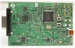


 工商网监
湘ICP备2023018690号
工商网监
湘ICP备2023018690号
