User's Guide
SLUUBF6 – April 2016
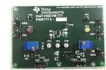
bq21040 0.8-A Single-Input, Single-Cell Li-Ion Battery
Charger Evaluation Module
This user’s guide describes the bq21040 evaluation module (EVM), how to perform a stand-alone
evaluation or interface with a host or system. The charger is designed to deliver up to 800 mA of
continuous current to the battery output when programmed with a resistor on the ISET pin and is
programmed at the factory for approximately 540 mA. The charge status is indicated by the /CHG pin.
1
2
3
4
5
Contents
Introduction ...................................................................................................................
Considerations With Evaluating the bq21040 ............................................................................
Performance Specification Summary .....................................................................................
Test Summary ................................................................................................................
4.1
Equipment ...........................................................................................................
4.2
Equipment and EVM Setup........................................................................................
4.3
Test Procedure Using a Single Cell Li-Ion Battery .............................................................
4.4
Alternate Test Methods ............................................................................................
Schematic, Physical Layouts and Bill of Materials ......................................................................
5.1
Schematic ............................................................................................................
5.2
Physical Layouts ....................................................................................................
5.3
Bill of Materials ......................................................................................................
2
2
2
2
3
3
4
4
5
5
6
7
List of Figures
1
EVM Setup.................................................................................................................... 3
2
bq21040 EVM Board Schematic ........................................................................................... 5
3
Assembly Layer .............................................................................................................. 6
4
Top Layer ..................................................................................................................... 6
5
Bottom Layer ................................................................................................................. 6
SLUUBF6 – April 2016
Submit Documentation Feedback
bq21040 0.8-A Single-Input, Single-Cell Li-Ion Battery Charger Evaluation
Module
Copyright © 2016, Texas Instruments Incorporated
1
�Introduction
1
www.ti.com
Introduction
The bq21040 series of devices are highly integrated Li-ion linear charger devices targeted at space-limited
portable applications. The devices operate from either a USB port or AC adapter.
The bq21040 has a single power output that charges the battery. A system load can be placed in parallel
with the battery as long as the average system load does not keep the battery from charging fully during
the 10 hour safety timer.
The battery is charged in three phases: conditioning, constant current, and constant voltage. In all charge
phases, an internal control loop monitors the IC junction temperature and reduces the charge current if an
internal temperature threshold is exceeded.
The charger power stage and charge current sense functions are fully integrated. The charger function
has high-accuracy current and voltage regulation loops, charge status display, and charge termination.
The pre-charge current and termination current threshold are set to 20% and 10% of the fast charge
current internally on the bq21040. The fast charge current value is programmable via an external resistor.
2
Considerations With Evaluating the bq21040
Refer to the bq21040 data sheet (SLUSCE2) for specific details on the charger ICs.
The ISET current control loop sets the maximum charge current. A system load may be connected to the
OUT pin, which takes away some of the charge current. Normally it is not recommended to operate the
device in pre-charge since the system load keeps the battery from recovering; but, since the precharge
current is fixed to 20% of its fast charge current, this restriction is not necessary.
3
Performance Specification Summary
Specification
Test Conditions
MIN
Input DC voltage, Vin
Recommended input voltage range
Reduced Performance, Vin (1)
Will not charge with Over Voltage input condition. Limited
charging with under voltage input.
Power Dissipation (2)
PDISS = (VIN – VOUT) × IOUT
IOUT
RISET = 1 kΩ
(1)
(2)
4
TYP
MAX
UNIT
4.45
6.45
V
3.5
28
V
1.5
W
0.8
A
0.54
Input voltage range is specified for normal operation. Input voltage between UVLO and 4.75 V has limited functionality, but does
not damage the IC nor present any safety issue with the battery. Input voltage above OVP and less than 30 Vdc has no
operation and will not damage the IC. Lower input voltage (closer to dropout operation) produces less heat dissipation and
potentially better performance.
The junction temperature rise above ambient is proportional to the power dissipation. Once the junction temperature reaches
approximately 125°C, thermal regulations reduces the programmed charge current.
Test Summary
The bq21040 EVM board requires a 5-VDC, 1-A power source to provide input power and a single-cell Liion or Li-polymer battery pack. The test setup connections and jumper setting selections are configured for
a stand-alone evaluation; but, can be changed to interface with external hardware such as a
microcontroller.
2
bq21040 0.8-A Single-Input, Single-Cell Li-Ion Battery Charger Evaluation
Module
Copyright © 2016, Texas Instruments Incorporated
SLUUBF6 – April 2016
Submit Documentation Feedback
�Test Summary
www.ti.com
4.1
Equipment
•
•
•
•
4.2
Power supply +5.1 ±0.1 V, current limit set to 1.5 ±0.1 A
Battery: 4.2-V LiCoO2 or equivalent
Three Fluke 75 DMMs (equivalent or better)
Oscilloscope, model TDS220 (equivalent or better)
Equipment and EVM Setup
Jack or Component
Connect or Adjustment To:
J1 – VIN
Power supply positive, preset to 5 VDC, 1-A current limit
J2 – GND
Power supply ground
J3 – OUT
Positive Battery Pack Terminal
J4 – GND
Negative Battery Pack Terminal
J5 - TS
No shunt
JP1
No shunt
JP2
Apply shunt for CHG LED connection, CHG = OUT
JP3
Apply shunt for TS connection
R2 (RISET)
Adjust R2 for 1 kΩ between TP2 and GND
R11 ( RTS)
Adjust R11 for 10 kΩ between TP9 and GND
TP1
TP3
J1
5.1 VDC
VIN
IN (DC +)
CH1
GND (DC -)
P/S
#1
VIN
OUT
U1
6
J3
IN
DNPC2
10µF
C1
1µF
TP7
GND
4
OUT
2
TS
1
CHG
3
VSS
5
ISET
OUT
TP6
C3
2.2µF
TP5
TP4
J4
JP3
GND
GND
GND
R1
680
DNPC4
10µF
BQ21040DBV
GND
D2
Green
TP8
J5
GND
R2
TS
R3
1.50k
OUT (BAT +)
GND (BAT -)
GND
GND
Li-Ion
Cell
GND
R6
1.00k
3
2
1
10k Ohm
TP2
R4
10.0k
GND
GND
JP1
R7
HIGH
TS
GND
J2
GND
C5
0.1µF
50k
GND
GND
GND
R5
OUT
VIN
3
2
1
1.00k
D1
5.6V
OUT
CHG
VIN
JP2
GND
Dashed Line Represents EVM Board
Figure 1. EVM Setup
SLUUBF6 – April 2016
Submit Documentation Feedback
bq21040 0.8-A Single-Input, Single-Cell Li-Ion Battery Charger Evaluation
Module
Copyright © 2016, Texas Instruments Incorporated
3
�Test Summary
4.3
www.ti.com
Test Procedure Using a Single Cell Li-Ion Battery
1. Verify that the setup is correct and turn on the power supply, which was preset to 5 VDC, and 1 A for
the current-limit setting.
2. The bq21040 enters preconditioning mode if the battery is below the V(LOWV) threshold. In this mode,
the bq21040 pre-charges the battery with a low current (internally set to 20% of fast charge) until the
battery voltage reaches the V(LOWV) threshold or until the pre-charge timer expires. If the timer expires,
then the charge current is terminated and the bq21040 enters fault mode. The CHG LED turns off
when in timer fault mode. Toggling input power, toggling TS (BAT_EN) or battery replacement resets
fault mode.
3. When the battery voltage rises above the V(LOWV) threshold, the battery enters fast-charge constant
current mode. This EVM is programmed for 0.54 A of fast-charging current.
4. Once the battery reaches the voltage regulation threshold (4.2 V), the voltage control loop takes over
and the current tapers down as the battery reaches its full capacity.
5. The battery remains at the fast-charge mode until either the charge timer expires or the charge
termination current threshold is reached.
6. When the charge terminates, the CHG LED turns off.
7. Remove JMP3 (TS) and the charger turns on. This mode is Termination and Timer Disable Mode
(TTDM). This allows continuous power applied from the input to the output, regulated to 4.2 V with a
maximum current programmed by the ISET resistor. The system can operate without a battery in this
mode as long as the system does not exceed the supplied input current.
8. If the battery discharges to the recharge threshold, the charger starts fast charging, but the CHG LED
will not come on for the subsequent charges. Cycling the input power, replacing the battery, or toggling
the TS pin low starts a new charge with the CHG LED on.
9. Install the jumper on JP3 (TS) adjust R7 until VTS (voltage between TPS and GND) is around 1.23 V.
Charging should be suspended. Reduce voltage on TS pin by adjust R7 until charging resumes.
Further reduce the voltage on TS until VTS is around 278 mV and charging should be suspended.
NOTE: Loads across the battery can affect termination. The pre-term pin can be adjusted to offset
the system current. See data sheet for more details.
4.4
Alternate Test Methods
A 4-quadrant power supply that can source and sink current can be used in place of the battery pack to
evaluate the charger. It allows each transfer between pre-charge, constant-current and constant voltage
fast charge. Keep leads short to avoid adding too much inductance which may cause an interaction
between the power supply and charger. A large capacitor across the output helps cancel the inductance if
long leads are necessary.
4
bq21040 0.8-A Single-Input, Single-Cell Li-Ion Battery Charger Evaluation
Module
Copyright © 2016, Texas Instruments Incorporated
SLUUBF6 – April 2016
Submit Documentation Feedback
�Schematic, Physical Layouts and Bill of Materials
www.ti.com
5
Schematic, Physical Layouts and Bill of Materials
5.1
Schematic
Figure 2 illustrates the EVM schematic.
TP1
TP3
J1
VIN
VIN
6
J2
TP2
OUT
U1
J3
IN
DNPC2
10µF
C1
1µF
TP7
4
2
TS
1
CHG
3
VSS
5
ISET
GND
GND
OUT
OUT
TP6
C3
2.2µF
TP5
J4
GND
GND
BQ21040DBV
GND
D2
Green
TP8
GND
TP4
JP3
GND
R1
680
DNPC4
10µF
J5
GND
R2
TS
R3
1.50k
R4
10.0k
GND
JP1
R7
HIGH
TS
GND
GND
GND
R6
1.00k
3
2
1
10k Ohm
GND
C5
0.1µF
50k
GND
GND
GND
R5
OUT
VIN
3
2
1
1.00k
D1
5.6V
OUT
CHG
VIN
JP2
GND
Figure 2. bq21040 EVM Board Schematic
SLUUBF6 – April 2016
Submit Documentation Feedback
bq21040 0.8-A Single-Input, Single-Cell Li-Ion Battery Charger Evaluation
Module
Copyright © 2016, Texas Instruments Incorporated
5
�Schematic, Physical Layouts and Bill of Materials
5.2
www.ti.com
Physical Layouts
Figure 3 through Figure 5 illustrate the EVM PCB layouts.
Figure 3. Assembly Layer
Figure 4. Top Layer
Figure 5. Bottom Layer
6
bq21040 0.8-A Single-Input, Single-Cell Li-Ion Battery Charger Evaluation
Module
Copyright © 2016, Texas Instruments Incorporated
SLUUBF6 – April 2016
Submit Documentation Feedback
�Schematic, Physical Layouts and Bill of Materials
www.ti.com
5.3
Bill of Materials
Table 1 lists the EVM BOM.
Table 1. bq21040EVM Bill of Materials
Designator
Qty
Value
Description
PackageReference
PartNumber
Manufacturer
Alternate PartNumber
Alternate
Manufacturer
!PCB
1
C1
1
1uF
CAP, CERM, 1 µF, 25 V, +/- 10%, X5R, 0603
0603
PWR777
Any
-
-
C1608X5R1E105K080AC
TDK
C3
1
2.2uF
CAP, CERM, 2.2 µF, 10 V, +/- 10%, X7R, 0603
C5
1
0.1uF
CAP, CERM, 0.1uF, 50V, +/-10%, X7R, 0603
0603
GRM188R71A225KE15D
Murata
0603
GCM188R71H104KA57B
D1
1
5.6V
Murata
Diode, Zener, 5.6 V, 225 mW, SOT-23
SOT-23
BZX84C5V6LT1G
D2
1
Green
ON Semiconductor
LED, Green, SMD
1.6x0.8x0.8mm
LTST-C190GKT
J1, J2, J3, J4, J5,
JP3
Lite-On
6
Header, 100mil, 2x1, Tin plated, TH
Header, 2 PIN, 100mil,
Tin
PEC02SAAN
Sullins Connector Solutions
JP1, JP2
2
Header, 100mil, 3x1, Tin plated, TH
Header, 3 PIN, 100mil,
Tin
PEC03SAAN
Sullins Connector Solutions
R1
1
680
RES, 680, 5%, 0.1 W, 0603
0603
CRCW0603680RJNEA
Vishay-Dale
R2
1
10k Ohm
Trimmer, 10k ohm, 0.25W, TH
4.5x8x6.7mm
3266W-1-103LF
Bourns
R3
1
1.50k
RES, 1.50k ohm, 1%, 0.1W, 0603
0603
CRCW06031K50FKEA
Vishay-Dale
Equivalent
Any
R4
1
10.0k
RES, 10.0 k, 0.1%, 0.1 W, 0603
0603
RT0603BRD0710KL
Yageo America
R5, R6
2
1.00k
RES, 1.00 k, 1%, 0.1 W, 0603
0603
CRCW06031K00FKEA
Vishay-Dale
R7
1
50k
Trimmer, 50k ohm, 0.25W, TH
4.5x8x6.7mm
3266W-1-503LF
Bourns
SH-JP1, SH-JP2,
SH-JP3
3
1x2
Shunt, 100mil, Gold plated, Black
Shunt
969102-0000-DA
3M
SNT-100-BK-G
Samtec
TP1
1
Red
Test Point, Miniature, Red, TH
Red Miniature Testpoint
5000
Keystone
TP2, TP4, TP8
3
Black
Test Point, Miniature, Black, TH
Black Miniature Testpoint
5001
Keystone
TP3
1
Yellow
Test Point, Miniature, Yellow, TH
Yellow Miniature
Testpoint
5004
Keystone
TP5, TP6, TP7
3
White
Test Point, Miniature, White, TH
White Miniature Testpoint
5002
Keystone
U1
1
Single-Input, Low Cost Single Cell Li-Ion and Li-Pol
Battery Charger, DBV0006A
DBV0006A
BQ21040DBV
Texas Instruments
C2, C4
0
CAP, CERM, 10 µF, 25 V, +/- 10%, X5R, 0805
0805
C2012X5R1E106K125AB
TDK
FID1, FID2, FID3
0
Fiducial mark. There is nothing to buy or mount.
Fiducial
N/A
N/A
Printed Circuit Board
10uF
Notes:
SLUUBF6 – April 2016
Submit Documentation Feedback
Texas Instruments
Unless otherwise noted in the Alternate Part Number and/or Alternate Manufacturer columns, all parts may be substituted with equivalents.
bq21040 0.8-A Single-Input, Single-Cell Li-Ion Battery Charger Evaluation
Module
Copyright © 2016, Texas Instruments Incorporated
7
�IMPORTANT NOTICE
Texas Instruments Incorporated and its subsidiaries (TI) reserve the right to make corrections, enhancements, improvements and other
changes to its semiconductor products and services per JESD46, latest issue, and to discontinue any product or service per JESD48, latest
issue. Buyers should obtain the latest relevant information before placing orders and should verify that such information is current and
complete. All semiconductor products (also referred to herein as “components”) are sold subject to TI’s terms and conditions of sale
supplied at the time of order acknowledgment.
TI warrants performance of its components to the specifications applicable at the time of sale, in accordance with the warranty in TI’s terms
and conditions of sale of semiconductor products. Testing and other quality control techniques are used to the extent TI deems necessary
to support this warranty. Except where mandated by applicable law, testing of all parameters of each component is not necessarily
performed.
TI assumes no liability for applications assistance or the design of Buyers’ products. Buyers are responsible for their products and
applications using TI components. To minimize the risks associated with Buyers’ products and applications, Buyers should provide
adequate design and operating safeguards.
TI does not warrant or represent that any license, either express or implied, is granted under any patent right, copyright, mask work right, or
other intellectual property right relating to any combination, machine, or process in which TI components or services are used. Information
published by TI regarding third-party products or services does not constitute a license to use such products or services or a warranty or
endorsement thereof. Use of such information may require a license from a third party under the patents or other intellectual property of the
third party, or a license from TI under the patents or other intellectual property of TI.
Reproduction of significant portions of TI information in TI data books or data sheets is permissible only if reproduction is without alteration
and is accompanied by all associated warranties, conditions, limitations, and notices. TI is not responsible or liable for such altered
documentation. Information of third parties may be subject to additional restrictions.
Resale of TI components or services with statements different from or beyond the parameters stated by TI for that component or service
voids all express and any implied warranties for the associated TI component or service and is an unfair and deceptive business practice.
TI is not responsible or liable for any such statements.
Buyer acknowledges and agrees that it is solely responsible for compliance with all legal, regulatory and safety-related requirements
concerning its products, and any use of TI components in its applications, notwithstanding any applications-related information or support
that may be provided by TI. Buyer represents and agrees that it has all the necessary expertise to create and implement safeguards which
anticipate dangerous consequences of failures, monitor failures and their consequences, lessen the likelihood of failures that might cause
harm and take appropriate remedial actions. Buyer will fully indemnify TI and its representatives against any damages arising out of the use
of any TI components in safety-critical applications.
In some cases, TI components may be promoted specifically to facilitate safety-related applications. With such components, TI’s goal is to
help enable customers to design and create their own end-product solutions that meet applicable functional safety standards and
requirements. Nonetheless, such components are subject to these terms.
No TI components are authorized for use in FDA Class III (or similar life-critical medical equipment) unless authorized officers of the parties
have executed a special agreement specifically governing such use.
Only those TI components which TI has specifically designated as military grade or “enhanced plastic” are designed and intended for use in
military/aerospace applications or environments. Buyer acknowledges and agrees that any military or aerospace use of TI components
which have not been so designated is solely at the Buyer's risk, and that Buyer is solely responsible for compliance with all legal and
regulatory requirements in connection with such use.
TI has specifically designated certain components as meeting ISO/TS16949 requirements, mainly for automotive use. In any case of use of
non-designated products, TI will not be responsible for any failure to meet ISO/TS16949.
Products
Applications
Audio
www.ti.com/audio
Automotive and Transportation
www.ti.com/automotive
Amplifiers
amplifier.ti.com
Communications and Telecom
www.ti.com/communications
Data Converters
dataconverter.ti.com
Computers and Peripherals
www.ti.com/computers
DLP® Products
www.dlp.com
Consumer Electronics
www.ti.com/consumer-apps
DSP
dsp.ti.com
Energy and Lighting
www.ti.com/energy
Clocks and Timers
www.ti.com/clocks
Industrial
www.ti.com/industrial
Interface
interface.ti.com
Medical
www.ti.com/medical
Logic
logic.ti.com
Security
www.ti.com/security
Power Mgmt
power.ti.com
Space, Avionics and Defense
www.ti.com/space-avionics-defense
Microcontrollers
microcontroller.ti.com
Video and Imaging
www.ti.com/video
RFID
www.ti-rfid.com
OMAP Applications Processors
www.ti.com/omap
TI E2E Community
e2e.ti.com
Wireless Connectivity
www.ti.com/wirelessconnectivity
Mailing Address: Texas Instruments, Post Office Box 655303, Dallas, Texas 75265
Copyright © 2016, Texas Instruments Incorporated
�