bq24350
bq24352
www.ti.com............................................................................................................................................................... SLUS943A – MAY 2009 – REVISED JUNE 2009
Over-Voltage and Over-Current Charger Front-end
Protection IC With Integrated Charging FET
Check for Samples: bq24350 bq24352
FEATURES
1
•
2
•
•
•
Robust Protection
– Input Over-Voltage Protection
– Input Over-Current Protection
– Accurate Battery Over-Voltage Protection
– Thermal Shutdown
– Output Short-Circuit Protection
Integrated Charging FET
LDO Mode Operation
Current Limited Power Supply for Host
Controller
•
•
•
•
•
Soft-Start to Prevent Inrush Currents
Soft-Stop to Prevent Voltage Spikes
30V Maximum Input Voltage
Supports Up to 1A Load Current
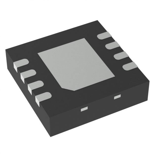
Small 2mm × 2mm 8pin SON Package
APPLICATIONS
•
•
Mobile Phones
Low-Power Handheld Devices
DESCRIPTION
The bq24350/2 is a highly integrated circuit designed to provide protection to Li-ion batteries from failures of the
charging circuit. The IC continuously monitors the input voltage and the battery voltage. In case of an input
over-voltage condition, the IC will turn off the internal power FET after a blanking time. If the battery voltage rises
to unsafe levels during charging process, power is removed from the system. If the input current exceeds the
over current threshold for a limited time, the IC will turn off the output power. The integrated charging FET can
regulate the charge voltage and current according to the control from the host. The device can also provide a
voltage source with over voltage and over current protection for host controller.
WHITE SPACE
WHITE SPACE
WHITE SPACE
TYPICAL APPLICATION CIRCUIT
WHITE SPACE
PIN ASSIGNMENT
WHITE SPACE
Analog
Base Band
Chip
CHGIN
bq24350 /2
ACIN
CHG IN
AC
CACIN
CCHGIN
Q1
1 mF
ACIN
1
8
OUT
ACIN
2
7
OUT
GND
3
6
CHGIN
VBAT
4
5
GATDRV
1 mF
Q2
GATDRV
GATDRV
OUT
ISENS
0 .2 W
GND
VBAT
R BAT
200 kW
VBAT
PACK+
PACK-
1
2
Please be aware that an important notice concerning availability, standard warranty, and use in critical applications of Texas
Instruments semiconductor products and disclaimers thereto appears at the end of this data sheet.
PowerPAD is a trademark of Texas Instruments.
PRODUCTION DATA information is current as of publication date.
Products conform to specifications per the terms of the Texas
Instruments standard warranty. Production processing does not
necessarily include testing of all parameters.
Copyright © 2009, Texas Instruments Incorporated
�bq24350
bq24352
SLUS943A – MAY 2009 – REVISED JUNE 2009............................................................................................................................................................... www.ti.com
These devices have limited built-in ESD protection. The leads should be shorted together or the device placed in conductive foam
during storage or handling to prevent electrostatic damage to the MOS gates.
SIMPLIFIED FUNCTION BLOCK DIAGRAM
Q2
Q1
VACIN
ACIN
V OUT
OUT
IIN
Protection &
Gate Control
+
-
IO(OCP)
INPUT UVLO
VACIN
+
VUVLO
-
t BLK ( CHGIN )
VCHGIN
+
INPUT OVP
GND
VACIN
+
VOVP
-
-
t DGL(OVP )
Control
CHGIN
VOREG
500 W
L ogic
VACIN
+
V OUT
-
V BAT
+
BVOVP
-
CHGIN Discharge
SLEEP
Battery OVP
VBAT
Protection
Control
t DGL (BOVP )
GATDRV
Thermal
Shutdown
VBAT
PIN FUNCTIONS
PIN
NAME
NUMBER
I/O
ACIN
1,2
I
Power Supply Input, connect to an external DC supply. Connect an external 1μF ceramic capacitor
(minimum) to GND.
OUT
7,8
O
Output terminal to the charging system.
VBAT
4
I
Battery voltage sense input. Connected to pack positive terminal through a resistor. Connected to
ground if battery OVP function is not used.
GATDRV
5
I
P-FET gate drive input , connected to gate drive pin of the host charger controller
CHGIN
6
O
Output power pin for power input of host charger controller. Connect an external ceramic bypass
capacitor (1.0μF minimum) to GND.
GND
3
–
Ground terminal
Thermal PAD
DESCRIPTION
There is an internal electrical connection between the exposed thermal pad and the GND pin of the
device. The thermal pad must be connected to the same potential as the GND pin on the printed circuit
board. Do not use the thermal pad as the primary ground input for the device. GND pin must be
connected to ground at all times.
ORDERING INFORMATION
2
PART NUMBER
MARKING
MEDIUM
QUANTITY
PACKAGE
INPUT OVP
THRESHOLD
bq24350DSGR
OAJ
Tape and Reel
3000
2mm × 2mm SON
6.17 V
bq24350DSGT
OAJ
Tape and Reel
250
2mm × 2mm SON
6.17 V
bq24352DSGR
OCY
Tape and Reel
3000
2mm × 2mm SON
7.1 V
bq24352DSGT
OCY
Tape and Reel
250
2mm × 2mm SON
7.1 V
Submit Documentation Feedback
Copyright © 2009, Texas Instruments Incorporated
Product Folder Link(s): bq24350 bq24352
�bq24350
bq24352
www.ti.com............................................................................................................................................................... SLUS943A – MAY 2009 – REVISED JUNE 2009
ABSOLUTE MAXIMUM RATINGS (1)
over operating free-air temperature range (unless otherwise noted)
VALUE / UNIT
Input voltage
ACIN (with respect to GND)
–0.3 V to 30 V
Output voltage
OUT, CHGIN (with respect to GND)
–0.3 V to 7V
Input voltage
VBAT, GATDRV (with respect to GND)
–0.3 V to 7 V
Input current
ACIN
–1.8 A (2) to 1.4 A
Junction temperature, TJ
–40°C to 150°C
Storage temperature, TSTG
–65°C to 150°C
(1)
(2)
Stresses beyond those listed under absolute maximum ratings may cause permanent damage to the device. These are stress ratings
only, and functional operation of the device at these or any other conditions beyond those indicated under recommended operating
conditions is not implied. Exposure to absolute-maximum-rated conditions for extended periods may affect device reliability. All voltage
values are with respect to the network ground terminal unless otherwise noted.
Reverse current is specified for a maximum of 50 hours at TJ < 150°C.
PACKAGE DISSIPATION RATINGS
PACKAGE
PACKAGE DRAWING
RθJC
RθJA
SON-8
DSG
5°C/W
75°C/W
RECOMMENDED OPERATING CONDITIONS
VACIN
ACIN voltage range
IACIN
Current, ACIN pin
TJ
Junction Temperature
MIN
MAX
4.4
15
–40
UNITS
A
125
°C
Submit Documentation Feedback
Copyright © 2009, Texas Instruments Incorporated
Product Folder Link(s): bq24350 bq24352
V
1
3
�bq24350
bq24352
SLUS943A – MAY 2009 – REVISED JUNE 2009............................................................................................................................................................... www.ti.com
ELECTRICAL CHARACTERISTICS
Refer to the typical application circuit shown in Figure 1 . These specifications apply over ACIN=5V, TJ = -40~125°C, unless
otherwise specified. Typical values are at TJ = 25°C.
PARAMETER
TEST CONDITIONS
MIN
TYP
MAX
ACIN: 3V → 2V, ACIN falling
1.8
1.95
2.1
ACIN: 2V → 3V, ACIN rising
2.5
UNIT
ACIN
VUVLO
Under-voltage lock-out threshold
tBLK(CHGIN)
Input power on blanking time
VACIN rising to CHGIN rising
IDD
Operating current
No load on OUT and CHGIN pin
10
V
ms
500
μA
INPUT TO OUTPUT CHARACTERISTICS
On resistance from ACIN to OUT
IOUT = 1.0A, ACIN=5V, GATDRV=0V
415
685
mΩ
On resistance from ACIN to CHGIN
ICHGIN = 1.0A, ACIN=5V, IOUT=0A
250
495
mΩ
5.33
5.5
5.66
V
6
6.17
6.35
6.9
7.1
7.3
250
300
350
100
150
200
INPUT OVER-VOLTAGE PROTECTION (OVP)
VOREG
ACIN=5.9V, GATDRV=CHGIN, ICHGIN=0 to
1A.
CHGIN voltage in LDO mode
Input OVP threshold, bq24350
VOVP
VACIN rising
Input OVP threshold, bq24352
VHYS-OVP
Input OVP recovery hysteresis, bq24350
Input OVP recovery hysteresis, bq24352
VACIN: 7.5V → 5V
V
mV
tDGL(OVP)
Input OVP deglitch time
VACIN rising to CHGIN falling
256
μS
tREC(OVP)
Input OVP recovery time
VACIN falling below VOVP to CHGIN rising
8.2
ms
INPUT OVER CURRENT LIMITING AND PROTECTION (OCP)
IO(OCP)
OCP threshold
1.02
1.2
1.38
A
tDGL(OCP)
OCP blanking time
8.2
ms
tREC(OCP)
OCP recovery time
131
ms
BATTERY OVER-VOLTAGE PROTECTION
BVOVP
Battery OVP threshold
VBAT rising
4.3
4.35
4.4
V
VHYS-BOVP
Battery OVP hysteresis
VBAT falling
200
250
300
mV
IVBAT
VBAT pin leakage current
VBAT=4.25V, series connection of a 200kΩ
resistor, TJ = 25°C
10
nA
tDGL(BOVP)
Battery OVP deglitch time
VBAT rising to CHGIN falling
8.2
ms
tREC(BOVP)
Battery OVP recovery time
VBAT falling below BVOVP to CHGIN rising
131
ms
VSEXIT
Sleep mode exit threshold and CHGIN turn
on threshold, ACIN-VOUT
ACIN rising, VOUT = 4.2 V
24
90
160
mV
VSENTRY
Sleep mode entry threshold and CHGIN turn
off threshold, ACIN-VOUT
ACIN falling, VOUT = 4.2 V
10
55
105
mV
IDDSLP
Sleep Mode supply current
OUT = 4.2 V, GATDRV = 4.2 V,
ACIN = VSS
10
μA
RDIS
CHGIN discharge resistor
CHGIN
Ω
500
Leakage current from OUT to CHGIN
OUT = 4.2 V, GATDRV = 4.2 V, CHGIN = 0
V, ACIN = 0 V, TJ = 85°C
1
μA
680
800
mV
0.1
1
μA
INTEGRATED P-FET PARAMETERS
Vt
Threshold Voltage, CHGIN-GATDRV.
CHGIN=5V, OUT=3.6V, IOUT=10mA
500
Ig
GATDRV pin leakage current
Ioff
Off state leakage current at OUT pin.
ACIN=5V, GATDRV=CHGIN, OUT=0V
Ronp
On Resistance of P-FET (from CHGIN to
OUT)
IOUT = 1.0A, ACIN=5V, GATDRV=0V
Gm
Forward Transconductance
ACIN=5V, IOUT=5mA, GATDRV=3.5V
Cg
Input capacitance at the GATDRV pin
CHGIN=GATDRV=5V
μA
1
165
225
mΩ
27
mA/V
104
pF
THERMAL PROTECTION
TJ(OFF)
4
Thermal shutdown threshold
Junction temperature rising
Submit Documentation Feedback
140
150
160
°C
Copyright © 2009, Texas Instruments Incorporated
Product Folder Link(s): bq24350 bq24352
�bq24350
bq24352
www.ti.com............................................................................................................................................................... SLUS943A – MAY 2009 – REVISED JUNE 2009
ELECTRICAL CHARACTERISTICS (continued)
Refer to the typical application circuit shown in Figure 1 . These specifications apply over ACIN=5V, TJ = -40~125°C, unless
otherwise specified. Typical values are at TJ = 25°C.
PARAMETER
TEST CONDITIONS
TJ(OFF-HYS) Thermal shutdown hysteresis
MIN
TYP
Junction temperature falling
MAX
20
UNIT
°C
TYPICAL APPLICATION CIRCUIT
ACIN=5V, ICHARGE=1A, VBAT=4.2V
Analog
Base Band
Chip
bq24350/2
ACIN
CHGIN
AC
CHGIN
CACIN
CCHGIN
Q1
1 mF
1 mF
GATDRV
Q2
GATDRV
OUT
ISENS
0.2 W
GND
VBAT
R BAT
VBAT
200 kW
PACK+
PACK-
Figure 1. Host Controlled One-Cell Charger Application Circuit
TYPICAL PERFORMANCE CHARACTERISTICS
Using circuit shown in typical application circuit Figure 1, TA = 25°C, unless otherwise specified.
ACIN RAMP UP
ACIN RAMP DOWN
GATDRV 2 V/div
ACIN 2 V/div
CHGIN Pull Down
CHGIN 2 V/div
ACIN 2 V/div
Soft-Start
Soft-Stop
VACIN = 5.2 V, CHGIN = 4.5 V, ICHG = 0.6 A,
VGATDRV = 3.5 V, VBAT = 3.4 V
CHGIN 2 V/div
IACIN 0.5 A/div
IACIN 0.5 A/div
VACIN = 5.2 V, CHGIN = 4.5 V, ICHG = 0.6 A,
VGATDRV = 3.5 V, VBAT = 3.4 V
Time: 2 mS/div
Time: 1 mS/div
Figure 2.
Figure 3.
Submit Documentation Feedback
Copyright © 2009, Texas Instruments Incorporated
Product Folder Link(s): bq24350 bq24352
5
�bq24350
bq24352
SLUS943A – MAY 2009 – REVISED JUNE 2009............................................................................................................................................................... www.ti.com
TYPICAL PERFORMANCE CHARACTERISTICS (continued)
ACIN OVP (BLANKING TIME)
16 V
ACIN OVP
16 V
ACIN 5 V/div
ACIN 5 V/div
CHGIN 1 V/div
5V
CHGIN 1 V/div
5V
6V
5.5 V
VACIN = 5-16 V, Rising Time 0.5 ms
VACIN = 5-16 V, Rising Time 0.5 ms
ICHGIN 0.1 A/div
ICHGIN 0.1 A/div
Time: 1 ms/div
Time: 100 ms/div
Figure 4.
Figure 5.
ACIN OVP
CHGIN OCP
ACIN 5 V/div
VACIN = 5 V, ICHGIN = 0 to 1.3 A
VACIN = 5-16 V, Rising Time
0.5 ms, ICHGIN 2V/div
CHGIN 2 V/div
CHGIN 2 V/div
1.3 A
ICHGIN 0.5 A/div
ICHGIN 0.1 A/div
Time: 20 mS/div
Time: 100 mS/div
Figure 6.
Figure 7.
CHGIN OCP
BATTERY OVP
VBAT 2 V/div
Connect 3 W Load
CHGIN 2 V/div
VACIN = 5 V, ICHGIN = 0 to1.3 A
VACIN = 5 V, VBAT = 3.4 V to 5 V
ICHGIN 0.5 A/div
CHGIN 2 V/div
ICHGIN 0.1 A/div
6
Time: 2 mS/div
Time: 50 mS/div
Figure 8.
Figure 9.
Submit Documentation Feedback
Copyright © 2009, Texas Instruments Incorporated
Product Folder Link(s): bq24350 bq24352
�bq24350
bq24352
www.ti.com............................................................................................................................................................... SLUS943A – MAY 2009 – REVISED JUNE 2009
TYPICAL PERFORMANCE CHARACTERISTICS (continued)
Rdson vs Vgs
rdson - Static Drain-Source On-State Resistance - W
BATTERY OVP
VBAT 2 V/div
VACIN = 5 V, VBAT = 3.4 V to 5 V
CHGIN 2 V/div
IACIN 0.5 A/div
Time: 2 mS/div
10000
1000
VCHGIN = 5 V,
VCHGIN -VOUT = 200 mV
100
10
Q2
1
0.1
0
1000
2000
3000
Vgs - Vchgin-Vgatdrv - mV
Figure 10.
4000
5000
Figure 11.
rdson - Static Drain-Source On-State Resistance - mW
FET ON RESISTANCE vs TEMPERATURE
600
550
500
Q1 +Q2
450
400
350
Q1
300
250
Q2
200
150
100
-50
0
50
100
TJ - Junction Temperature - °C
150
Figure 12.
BACKGROUND
During the charging process for portable devices, input voltage spikes usually happen when the AC/DC adaptor
is plugged in, or charge current is cut off quickly under fault conditions, such as input OVP, OCP or battery OVP
and so on. The over voltage stress may damage the analog baseband chip which has lower voltage rating due to
its increased complexity. Therefore, over voltage protection is needed for the safe operation of portable devices.
Another challenge arises from the charge circuit that uses external charging FET in series with a reverse
blocking diode as the charging device. The battery may not be fully charged when input voltage is low due to the
additional diode voltage drop. bq24350/2 will provide the solution for above problems since it has input OVP,
OCP, battery OVP function, together with integrated charging FET which will eliminate the reverse blocking diode
in the previously mentioned charge circuit, as shown in Figure 1.
DETAILED FUNCTIONAL DESCRIPTION
The bq24350/2 is a highly integrated circuit designed to provide protection to Li-ion batteries from failures of the
charging circuit. The IC continuously monitors the input voltage and the battery voltage. In case of an input
over-voltage condition, the IC will turn off the internal power FET after a blanking time. If the battery voltage rises
to unsafe levels during charging process, power is removed from the system. If the input current exceeds the
over current threshold for a limited time, the IC will turn off the output power. The integrated charging FET can
regulate the charge voltage and current according to the control from the host. The device can also provide a
voltage source with over voltage and over current protection for host controller.
Submit Documentation Feedback
Copyright © 2009, Texas Instruments Incorporated
Product Folder Link(s): bq24350 bq24352
7
�bq24350
bq24352
SLUS943A – MAY 2009 – REVISED JUNE 2009............................................................................................................................................................... www.ti.com
POWER DOWN
The device remains in power down mode when the input voltage at the ACIN pin is below the under-voltage
threshold VUVLO. The FET Q1 and Q2 connected between ACIN and OUT pins are off.
POWER-ON RESET
The device resets when the input voltage at the ACIN pin exceeds the UVLO threshold. All internal counters and
other circuit blocks are reset. The IC then waits for duration tBLK(CHGIN) for the input voltage to stabilize. If, after
tBLK(CHGIN), the input voltage and battery voltage are in normal range, FET Q1 is turned ON. The IC has a
soft-start feature to control the inrush current. The soft-start minimizes the ringing at the input, where the ringing
occurs because the parasitic inductance of the adapter cable and the input bypass capacitor form a resonant
circuit. Once the soft-start sequence starts, the IC monitors the load current. If the load current is larger than
IO(OCP) for more than tDGL(OCP), FET Q1 and Q2 are switched off. The IC then repeats the power-on sequence
after tREC(OCP).
When a short-circuit is detected at power-on and Q1 is switched off, to prevent the input voltage from spiking up
due to resonance between the inductance of the input cable and the input capacitor, Q1 is turned off slowly by
reducing its gate-drive gradually, resulting in a “soft-stop”.
SLEEP MODE
When ACIN falls to below sleep mode entry threshold (VSENTRY), the device operates in sleep mode and turns off
Q1 and Q2 by internal circuit regardless of the gate drive signal from GARDRV pin. The device exits sleep mode
when ACIN rising to above sleep mode exit threshold (VSEXIT). In this way, the device behaves like a diode and
no external reverse blocking diode is needed in the application circuit.
OPERATING
The device continuously monitors the input voltage, the input current and the battery voltage as described in
detail below:
Input Over-Voltage Protection and LDO Mode Operation
The CHGIN output of the IC operates similar to a linear regulator. Figure 13 shows the typical input OVP
performance. When the ACIN input voltage is less than VO(REG), and above the VUVLO, the CHGIN output voltage
tracks the input voltage with a voltage drop caused by RDS(on) of the protection FET Q1. When the ACIN input
voltage is greater than VO(REG) plus the RDS(on) drop of Q1, and less than VOVP, the CHGIN output voltage is
regulated to VO(REG), and this is also referred as LDO mode operation. If the input voltage rises above VOVP, the
internal FET Q1 and Q2 are turned off after a blanking time of tDGL(OVP), removing power from the circuit. When
the input voltage drops below VOVP – VHYS-OVP, and is still above VUVLO, the FET Q1 and Q2 are turned on again
after a deglitch time of tREC(OVP) , which ensures that the input supply is stabilized when the IC starts up again.
VINVOREG
VOVP
VPOR
VO(REG)
CHGIN
tDGL(OVP)
tREC(OVP)
tBLK(CHGIN)
ACIN OVP
Figure 13. Input OVP Timing Diagram
Over Current Limiting and Protection
The device includes a low drop out linear current regulator. This current regulator uses Q1 as the controlling
8
Submit Documentation Feedback
Copyright © 2009, Texas Instruments Incorporated
Product Folder Link(s): bq24350 bq24352
�bq24350
bq24352
www.ti.com............................................................................................................................................................... SLUS943A – MAY 2009 – REVISED JUNE 2009
power device. Once the soft start sequence starts, the input current is limited to the Over Current Protection
(OCP) threshold, IO(OCP). If the input current through the IC attempts to exceed the OCP threshold, the switch Q1
is opened only enough to maintain the current at the OCP level. If the current limiting condition is maintained
longer than the deglitch time, tDGL(OCP), both the switch Q1 and Q2 are opened completely, as shown in
Figure 14. In this fault case, the switch Q1 is turned off slowly, typically taking 100μS.
Once the OCP feature has been activated, the switch Q1 and Q2 will remain off for the OCP recovery time,
tREC(OCP). Following this time the switch will turn on, using soft start sequence. If the current through the IC
remains below the OCP threshold, the switch will remain closed and normal operation resumes. If the current
through the IC attempts to exceed the OCP threshold again, the operation described above repeats.
IACIN
OCP
T hreshold
CHGIN
tDGL(OCP)
tREC(OCP)
tREC(OCP)
tDGL(OCP)
Figure 14. Charge Current OCP Timing Diagram
Battery Over-Voltage Protection
The battery over-voltage threshold, BVOVP, is internally set to 4.35V. If the battery voltage exceeds the BVOVP
threshold, the FET Q1 and Q2 are turned off after a deglitch time of tDGL(BOVP). The FET is turned on once the
battery voltage drops to BVOVP – VHYS-BOVP and remains below this threshold for tREC(BOVP), as shown in
Figure 15. In this battery over-voltage fault case, Q1 is switched OFF gradually for a smooth transient response.
VBAT
VBAT
OVP
CHGIN
tREC(BOVP)
tDGL(BOVP)
tDGL(BOVP)
tREC(BOVP)
Figure 15. Battery OVP Timing Diagram
Thermal Protection
If the junction temperature of the device exceeds TJ(OFF), the FET Q1 and Q2 are turned off. The FET is turned
back on when the junction temperature falls below TJ(OFF) – TJ(OFF-HYS).
Submit Documentation Feedback
Copyright © 2009, Texas Instruments Incorporated
Product Folder Link(s): bq24350 bq24352
9
�bq24350
bq24352
SLUS943A – MAY 2009 – REVISED JUNE 2009............................................................................................................................................................... www.ti.com
APPLICATION INFORMATION
Selection of RBAT
It is strongly recommended that the battery not be tied directly to the VBAT pin of the device, as under some
failure modes of the IC, the voltage at the ACIN pin may appear on the VBAT pin. This voltage can be as high as
30V, and applying 30V to the battery in case of the failure of the device can be hazardous. Connecting the VBAT
pin through RBAT prevents a large current from flowing into the battery in case of failure of the IC. In the interests
of safety, RBAT should have a very high value. The problem with a large RBAT is that the voltage drop across this
resistor because of the VBAT bias current IVBAT causes an error in the BVOVP threshold. This error is over and
above the tolerance on the nominal 4.35V BVOVP threshold.
Choosing RBAT in the range 100kΩ to 470kΩ is a good compromise. In the case of IC failure, with RBAT equal to
100kΩ, the maximum current flowing into the battery would be (30V – 3V) ÷ 100kΩ = 270μA, which is low
enough to be absorbed by the bias currents of the system components. RBAT equal to 100kΩ would result in a
worst-case voltage drop of RBAT × IVBAT 1mV. This is negligible compared to the internal tolerance of 50mV on
the BVOVP threshold.
If the Battery OVP function is not required, the VBAT pin should be connected to GND.
Selection of Input and Output Bypass Capacitors
The input capacitor CACIN is for decoupling, and serves an important purpose. Whenever there is a step change
downwards in the system load current, the inductance of the input cable causes the input voltage to spike up.
CACIN prevents the input voltage from overshooting to dangerous levels. It is strongly recommended that a
ceramic capacitor of at least 1μF be used at the input of the device. It should be located in close proximity to the
ACIN pin.
CCHGIN should also be a ceramic capacitor of at least 1μF, located close to the CHGIN pin. CCHGIN also serves as
the input decoupling capacitor for the charging circuit downstream of the protection IC.
PCB Layout Guidelines
1. This device is a protection device, and is meant to protect down-stream circuitry from hazardous voltages.
Potentially, high voltages may be applied to this IC. It has to be ensured that the edge-to-edge clearances of
PCB traces satisfy the design rules for the maximum voltages expected to be seen in the system.
2. The device uses SON packages with a PowerPAD ™ . For good thermal performance, the PowerPAD
should be thermally coupled with the PCB ground plane. In most applications, this will require a copper pad
directly under the IC. This copper pad should be connected to the ground plane with an array of thermal vias.
3. CACIN and CCHGIN should be located close to the IC. Other components like RBAT should also be located close
to the IC.
10
Submit Documentation Feedback
Copyright © 2009, Texas Instruments Incorporated
Product Folder Link(s): bq24350 bq24352
�PACKAGE OPTION ADDENDUM
www.ti.com
29-Apr-2022
PACKAGING INFORMATION
Orderable Device
Status
(1)
Package Type Package Pins Package
Drawing
Qty
Eco Plan
(2)
Lead finish/
Ball material
MSL Peak Temp
Op Temp (°C)
Device Marking
(3)
(4/5)
(6)
BQ24350DSGR
ACTIVE
WSON
DSG
8
3000
RoHS & Green
NIPDAUAG
Level-2-260C-1 YEAR
-40 to 85
OAJ
BQ24350DSGT
ACTIVE
WSON
DSG
8
250
RoHS & Green
NIPDAUAG
Level-2-260C-1 YEAR
-40 to 85
OAJ
BQ24352DSGR
ACTIVE
WSON
DSG
8
3000
RoHS & Green
NIPDAUAG
Level-2-260C-1 YEAR
-40 to 85
OCY
BQ24352DSGT
ACTIVE
WSON
DSG
8
250
RoHS & Green
NIPDAUAG
Level-2-260C-1 YEAR
-40 to 85
OCY
(1)
The marketing status values are defined as follows:
ACTIVE: Product device recommended for new designs.
LIFEBUY: TI has announced that the device will be discontinued, and a lifetime-buy period is in effect.
NRND: Not recommended for new designs. Device is in production to support existing customers, but TI does not recommend using this part in a new design.
PREVIEW: Device has been announced but is not in production. Samples may or may not be available.
OBSOLETE: TI has discontinued the production of the device.
(2)
RoHS: TI defines "RoHS" to mean semiconductor products that are compliant with the current EU RoHS requirements for all 10 RoHS substances, including the requirement that RoHS substance
do not exceed 0.1% by weight in homogeneous materials. Where designed to be soldered at high temperatures, "RoHS" products are suitable for use in specified lead-free processes. TI may
reference these types of products as "Pb-Free".
RoHS Exempt: TI defines "RoHS Exempt" to mean products that contain lead but are compliant with EU RoHS pursuant to a specific EU RoHS exemption.
Green: TI defines "Green" to mean the content of Chlorine (Cl) and Bromine (Br) based flame retardants meet JS709B low halogen requirements of


 工商网监
湘ICP备2023018690号
工商网监
湘ICP备2023018690号
