BQ25710
BQ25710
SLUSD20A – JULY 2018 – REVISED FEBRUARY
2021
SLUSD20A – JULY 2018 – REVISED FEBRUARY 2021
www.ti.com
BQ25710 SMBus Narrow VDC Buck-Boost Battery Charge Controller With System
Power Monitor and Processor Hot Monitor
1 Features
•
•
•
•
•
•
•
•
•
•
•
•
2 Applications
•
•
•
Ultra-Books, notebooks, detachable, tablet PCs
and power bank
Industrial and medical equipment
Portable equipment with rechargeable batteries
3 Description
This device is a synchronous NVDC buck-boost
battery charge controller, offering a low component
count, high efficiency solution for space constrained,
1s-4s battery charging applications.
Device Information
PACKAGE(1)
PART NUMBER
BQ25710
(1)
WQFN (32)
BODY SIZE (NOM)
4.00 mm × 4.00 mm
For all available packages, see the orderable addendum at
the end of the data sheet.
VSYS
Adapter
3.5V ± 24V
BATT
(1S-4S)
Q1
Q2
Q3
Q4
HIDRV1
SW1BTST1BTST2SW2
HIDRV2
LODRV1
LODRV2 SYS
VBUS
ACN
BATDRV
BQ25710
ACP
SRP
SRN
IADPT, IBAT,
PSYS, PROCHOT
•
•
SMBus
•
Pin-to-pin and software compatible to BQ25700A
Charge 1s to 4s battery from wide range of input
source
– 3.5-V to 24-V Input operating voltage
– Supports USB2.0, USB 3.0, USB 3.1 (Type C),
and USB Power Delivery (USB-PD) input
current settings
– Seamless transition among buck, buck-boost
and boost operations
– Input current and voltage regulation (IDPM and
VDPM) against source overload
Power/current monitor for CPU throttling
– Comprehensive PROCHOT profile, IMVP8/
IMVP9 compliant
– Input and battery current monitor
– System power monitor, IMVP8/IMVP9
compliant
Narrow voltage DC (NVDC) power path
management
– Instant-on with no battery or depleted battery
– Battery supplements system when adapter is
fully-loaded
– Battery MOSFET ideal diode operation in
supplement mode
Power up USB port from battery (USB OTG)
– 3-V to 20.8-V VOTG With 8-mV resolution
– Output current limit up to 6.4 A with 50-mA
resolution
TI patented Pass Through Mode (PTM) for system
power efficiency improvement and battery fast
charging
When system is powered by battery only, Vmin
Active Protection (VAP) mode supplements battery
from input capacitors during system peak power
spike
Input Current Optimizer (ICO) to extract max input
power
800-kHz or 1.2-MHz Programmable switching
frequency for 2.2-µH or 1.0-µH inductor
Host control interface for flexible system
configuration
– SMBus Port optimal system performance and
status reporting
– Hardware pin to set input current limit without
EC control
Integrated ADC to monitor voltage, current and
power
High accuracy for the regulation and monitor
– ±0.5% Charge voltage regulation
– ±2% Input/charge current regulation
– ±2% Input/charge current monitor
– ±4% Power monitor
Safety
– Thermal shutdown
– Input, system, battery overvoltage protection
– Input, MOSFET, inductor overcurrent protection
Low battery quiescent current
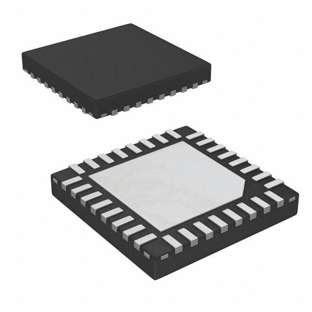
Package: 32-Pin 4 × 4 WQFN
Host
Application Diagram
An©IMPORTANT
NOTICEIncorporated
at the end of this data sheet addresses availability, warranty, changes, use in
safety-critical
applications,
Copyright
2021 Texas Instruments
Submit
Document
Feedback
intellectual property matters and other important disclaimers. PRODUCTION DATA.
Product Folder Links: BQ25710
1
�BQ25710
www.ti.com
SLUSD20A – JULY 2018 – REVISED FEBRUARY 2021
Table of Contents
1 Features............................................................................1
2 Applications..................................................................... 1
3 Description.......................................................................1
4 Revision History.............................................................. 2
5 Description (continued).................................................. 3
6 Device Comparison Table...............................................4
7 Pin Configuration and Functions...................................5
8 Specifications.................................................................. 8
8.1 Absolute Maximum Ratings........................................ 8
8.2 ESD Ratings............................................................... 8
8.3 Recommended Operating Conditions.........................8
8.4 Thermal Information....................................................9
8.5 Electrical Characteristics.............................................9
8.6 Timing Requirements................................................ 17
8.7 Typical Characteristics.............................................. 19
9 Detailed Description......................................................21
9.1 Overview................................................................... 21
9.2 Functional Block Diagram......................................... 22
9.3 Feature Description...................................................23
9.4 Device Functional Modes..........................................29
9.5 Programming............................................................ 30
9.6 Register Map.............................................................33
10 Application and Implementation................................ 68
10.1 Application Information........................................... 68
10.2 Typical Application.................................................. 68
11 Power Supply Recommendations..............................76
12 Layout...........................................................................77
12.1 Layout Guidelines................................................... 77
12.2 Layout Example...................................................... 78
13 Device and Documentation Support..........................79
13.1 Device Support....................................................... 79
13.2 Documentation Support.......................................... 79
13.3 Receiving Notification of Documentation Updates..79
13.4 Support Resources................................................. 79
13.5 Trademarks............................................................. 79
13.6 Electrostatic Discharge Caution..............................79
13.7 Glossary..................................................................79
14 Mechanical, Packaging, and Orderable
Information.................................................................... 80
4 Revision History
Changes from Revision * (July 2018) to Revision A (December 2020)
Page
• Changed units of measure for several parameters in Electrical Characteristics................................................ 9
• Changed in Timing Requirements.................................................................................................................... 17
• Added bullet 2 in Power-Up from DC Source................................................................................................... 23
• Changed 3.25A in Input Voltage and Current Limit Setup................................................................................ 23
• Changed in USB On-The-Go (OTG).................................................................................................................24
• Added in System Short Hiccup Mode............................................................................................................... 29
• Updated SMBus Interface.................................................................................................................................30
• Changed in ChargeOption0 Register................................................................................................................35
• Changed in ChargeOption2 Register................................................................................................................39
• Changed in ProchotOption0 Register............................................................................................................... 43
• Changed in ProchotStatus Register................................................................................................................. 50
• Changed in Input Current Registers................................................................................................................. 57
• Changed in IIN_DPM Register With 10-mΩ Sense Resistor............................................................................ 59
• Changed in ADCIINCMPIN Register................................................................................................................ 65
• Updated Typical Application Diagram...............................................................................................................68
• Updated ACP-ACN Input Filter Diagram.......................................................................................................... 69
• Updated Input Capacitor ..................................................................................................................................70
• Updated Output Capacitor................................................................................................................................ 70
• Changed in Layout Guidelines..........................................................................................................................77
• Added detailed layout reference in Layout Example........................................................................................ 78
2
Submit Document Feedback
Copyright © 2021 Texas Instruments Incorporated
Product Folder Links: BQ25710
�BQ25710
www.ti.com
SLUSD20A – JULY 2018 – REVISED FEBRUARY 2021
5 Description (continued)
The NVDC configuration allows the system to be regulated at battery voltage, but not drop below system
minimum voltage. The system keeps operating even when the battery is completely discharged or removed.
When load power exceeds input source rating, the battery goes into supplement mode and prevents the system
from crashing.
BQ25710 charges battery from a wide range of input sources including USB adapter, high voltage USB PD
sources and traditional adapters.
During power up, the charger sets converter to buck, boost or buck-boost configuration based on input source
and battery conditions. The charger automatically transits among buck, boost and buck-boost configuration
without host control.
In the absence of an input source, BQ25710 supports USB On-the-Go (OTG) function from 1- to 4-cell battery to
generate adjustable 3 V to 20.8 V on VBUS with 8 mV resolution. The OTG output voltage transition slew rate
can be configurable, which is complied with the USB PD 3.0 PPS specifications.
When only battery powers the system and no external load is connected to the USB OTG port, BQ25710
supports the Vmin Active Protection (VAP) feature, in which the device charges up the VBUS voltage from the
battery to store some energy in the input decoupling capacitors. During the system peak power spike, the huge
current drawing from the battery creates a larger voltage drop across the impedance from the battery to the
system. The energy stored in the input capacitors will supplement the system, to prevent the system voltage
from dropping below the minimum system voltage and causing the system crash. This Vmin Active Protection
(VAP) is designed to absorb system power peaks during periods of SOC high power demand, which is highly
recommended by Intel for the platforms with 1S~2S battery.
BQ25710 monitors adapter current, battery current and system power. The flexibly programmed PROCHOT
output goes directly to CPU for throttle back when needed.
Submit Document Feedback
Copyright © 2021 Texas Instruments Incorporated
Product Folder Links: BQ25710
3
�BQ25710
www.ti.com
SLUSD20A – JULY 2018 – REVISED FEBRUARY 2021
6 Device Comparison Table
4
BQ25700A
BQ25703A
BQ25708
BQ25710
BQ25718
BQ25713
BQ25713B
Interface
SMBus
I2C
SMBus
SMBus
SMBus
I2C
I2C
Device Address
09h
6Bh
09h
09h
09h
6Bh
6Ah
VAP for IMVP9
No
No
No
Yes
Yes
Yes
Yes
Pass Through Mode
No
No
No
Yes
Yes
Yes
Yes
OTG Mode
Yes
Yes
No
Yes
No
Yes
Yes
OTG Voltage Range
4.48V-20.8V
4.48V-20.8V
N/A
3.0V-20.8V
N/A
3.0V-20.8V
3.0V-20.8V
OTG Voltage
Resolution
64mV
64mV
N/A
8mV
N/A
8mV
8mV
Charging Voltage
Resolution
16mV
16mV
16mV
8mV
8mV
8mV
8mV
Submit Document Feedback
Copyright © 2021 Texas Instruments Incorporated
Product Folder Links: BQ25710
�BQ25710
www.ti.com
SLUSD20A – JULY 2018 – REVISED FEBRUARY 2021
SW1
HIDRV1
BTST1
LODRV1
REGN
PGND
LODRV2
BTST2
32
31
30
29
28
27
26
25
7 Pin Configuration and Functions
VBUS
1
24
HIDRV2
ACN
2
23
SW2
ACP
3
22
VSYS
CHRG_OK
4
21
BATDRV
OTG/VAP
5
20
SRP
ILIM_HIZ
6
19
SRN
VDDA
7
18
CELL_BATPRESZ
IADPT
8
17
COMP2
Thermal
11
12
13
14
15
16
SDA
SCL
CMPIN
CMPOUT
COMP1
10
PSYS
PROCHOT
9
IBAT
Pad
Figure 7-1. RSN Package 32-Pin WQFN Top View
Table 7-1. Pin Functions
PIN
NAME
NO.
I/O
DESCRIPTION
ACN
2
PWR
Input current sense resistor negative input. The leakage on ACP and ACN are matched. A
R-C low-pass filter is required to be placed between the sense resistor and the ACN pin to
suppress the high frequency noise in the input current signal. Refer to Section 10 for
ACP/ACN filter design.
ACP
3
PWR
Input current sense resistor positive input. The leakage on ACP and ACN are matched. A RC low-pass filter is required to be placed between the sense resistor and the ACP pin to
suppress the high frequency noise in the input current signal. Refer to Section 10 for
ACP/ACN filter design.
P-channel battery FET (BATFET) gate driver output. It is shorted to VSYS to turn off the
BATFET. It goes 10 V below VSYS to fully turn on BATFET. BATFET is in linear mode to
regulate VSYS at minimum system voltage when battery is depleted. BATFET is fully on
during fast charge and works as an ideal-diode in supplement mode.
BATDRV
21
O
BTST1
30
PWR
Buck mode high side power MOSFET driver power supply. Connect a 0.047-µF capacitor
between SW1 and BTST1. The bootstrap diode between REGN and BTST1 is integrated.
BTST2
25
PWR
Boost mode high side power MOSFET driver power supply. Connect a 0.047-μF capacitor
between SW2 and BTST2. The bootstrap diode between REGN and BTST2 is integrated.
CELL_BATPRESZ
18
I
Battery cell selection pin for 1–4 cell battery setting. CELL_BATPRESZ pin is biased from
VDDA. CELL_BATPRESZ pin also sets SYSOVP thresholds to 5 V for 1-cell, 12 V for 2-cell,
and 19.5 V for 3-cell/4-cell. CELL_BATPRESZ pin is pulled below VCELL_BATPRESZ_FALL to
indicate battery removal. The device exits LEARN mode, and disables charge. The charge
voltage register REG0x15() goes back to default.
Submit Document Feedback
Copyright © 2021 Texas Instruments Incorporated
Product Folder Links: BQ25710
5
�BQ25710
www.ti.com
SLUSD20A – JULY 2018 – REVISED FEBRUARY 2021
Table 7-1. Pin Functions (continued)
PIN
NAME
CHRG_OK
4
I/O
DESCRIPTION
O
Open drain active high indicator to inform the system good power source is connected to the
charger input. Connect to the pullup rail via 10-kΩ resistor. When VBUS rises above 3.5V or
falls below 24.5V, CHRG_OK is HIGH after 50ms deglitch time. When VBUS falls below 3.2
V or rises above 26 V, CHRG_OK is LOW. When any fault occurs, CHRG_OK is asserted
LOW.
CMPIN
14
I
Input of independent comparator. The independent comparator compares the voltage
sensed on CMPIN pin with internal reference, and its output is on CMPOUT pin. Internal
reference, output polarity and deglitch time is selectable by the SMBus host. With polarity
HIGH (REG0x30[6] = 1), place a resistor between CMPIN and CMPOUT to program
hysteresis. With polarity LOW (REG0x30[6] = 0), the internal hysteresis is 100 mV. If the
independent comparator is not in use, tie CMPIN to ground.
CMPOUT
15
O
Open-drain output of independent comparator. Place pullup resistor from CMPOUT to pullup
supply rail. Internal reference, output polarity and deglitch time are selectable by the SMBus
host.
COMP2
17
I
Buck boost converter compensation pin 2. Refer to BQ2571X EVM schematic for COMP2
pin RC network.
COMP1
16
I
Buck boost converter compensation pin 1. Refer to BQ2571X EVM schematic for COMP1
pin RC network.
OTG/VAP
5
I
Active HIGH to enable OTG or VAP modes. When REG0x32[5]=1, pulling high OTG/VAP pin
and setting REG0x32[12]=1 can enable OTG mode. When REG0x32[5]=0, pulling high
OTG/VAP pin is to enable VAP mode.
HIDRV1
31
O
Buck mode high side power MOSFET (Q1) driver. Connect to high side n-channel MOSFET
gate.
HIDRV2
24
O
Boost mode high side power MOSFET(Q4) driver. Connect to high side n-channel MOSFET
gate.
IADPT
8
O
The adapter current monitoring output pin. V(IADPT) = 20 or 40 × (V(ACP) – V(ACN)) with ratio
selectable in REG0x12[4]. Place a resistor from the IADPT pin to ground corresponding to
the inductance in use. For a 2.2 µH inductance, the resistor is 137 kΩ. Place a 100-pF or
less ceramic decoupling capacitor from IADPT pin to ground. IADPT output voltage is
clamped below 3.3 V.
IBAT
9
O
The battery current monitoring output pin. V(IBAT) = 8 or 16 × (V(SRP) – V(SRN)) for charge
current, or V(IBAT) = 8 or 16 × (V(SRN) – V(SRP)) for discharge current, with ratio selectable in
REG0x12[3]. Place a 100-pF or less ceramic decoupling capacitor from IBAT pin to ground.
This pin can be floating if not in use. Its output voltage is clamped below 3.3 V.
ILIM_HIZ
6
I
Input current limit setting pin. Program ILIM_HIZ voltage by connecting a resistor divider
from supply rail to ILIM_HIZ pin to ground. The pin voltage is calculated as: V(ILIM_HIZ) = 1 V
+ 40 × IDPM × RAC, in which IDPM is the target input current. The input current limit used
by the charger is the lower setting of ILIM_HIZ pin and REG0x3F(). When the pin voltage is
below 0.4 V, the device enters Hi-Z mode with low quiescent current. When the pin voltage is
above 0.8 V, the device is out of Hi-Z mode.
LODRV1
29
O
Buck mode low side power MOSFET (Q2) driver. Connect to low side n-channel MOSFET
gate.
LODRV2
26
O
Boost mode low side power MOSFET (Q3) driver. Connect to low side n-channel MOSFET
gate.
PGND
27
GND
PROCHOT
6
NO.
11
Device power ground.
O
Active low open drain output of processor hot indicator. It monitors adapter input current,
battery discharge current, and system voltage. After any event in the PROCHOT profile is
triggered, a pulse is asserted. The minimum pulse width is adjustable in REG0x21[14:11].
PSYS
10
O
Current mode system power monitor. The output current is proportional to the total power
from the adapter and the battery. The gain is selectable through SMBus. Place a resistor
from PSYS to ground to generate output voltage. This pin can be floating if not in use. Its
output voltage is clamped below 3.3 V. Place a capacitor in parallel with the resistor for
filtering.
REGN
28
PWR
6-V linear regulator output supplied from VBUS or VSYS. The LDO is active when VBUS
above VVBUS_CONVEN . Connect a 2.2- or 3.3-μF ceramic capacitor from REGN to power
ground. REGN pin output is for power stage gate drive.
Submit Document Feedback
Copyright © 2021 Texas Instruments Incorporated
Product Folder Links: BQ25710
�BQ25710
www.ti.com
SLUSD20A – JULY 2018 – REVISED FEBRUARY 2021
Table 7-1. Pin Functions (continued)
PIN
NAME
NO.
I/O
DESCRIPTION
SMBus clock input. Connect to clock line from the host controller or smart battery. Connect a
10-kΩ pullup resistor according to SMBus specifications.
SCL
13
I
SDA
12
I/O
SRN
19
PWR
Charge current sense resistor negative input. SRN pin is for battery voltage sensing as well.
Connect SRN pin with optional 0.1-μF ceramic capacitor to GND for common-mode filtering.
Connect a 0.1-μF ceramic capacitor from SRP to SRN to provide differential mode filtering.
The leakage current on SRP and SRN are matched.
SMBus open-drain data I/O. Connect to data line from the host controller or smart battery.
Connect a 10-kΩ pullup resistor according to SMBus specifications.
SRP
20
PWR
Charge current sense resistor positive input. Connect SRP pin with optional 0.1-uF ceramic
capacitor to GND for common-mode filtering. Connect a 0.1-μF ceramic capacitor from SRP
to SRN to provide differential mode filtering. The leakage current on SRP and SRN are
matched.
SW1
32
PWR
Buck mode high side power MOSFET driver source. Connect to the source of the high side
n-channel MOSFET.
SW2
23
PWR
Boost mode high side power MOSFET driver source. Connect to the source of the high side
n-channel MOSFET.
VBUS
1
PWR
Charger input voltage. An input low pass filter of 1Ω and 0.47 µF (minimum) is
recommended.
VDDA
7
PWR
Internal reference bias pin. Connect a 10-Ω resistor from REGN to VDDA and a 1-μF
ceramic capacitor from VDDA to power ground.
VSYS
22
PWR
Charger system voltage sensing. The system voltage regulation limit is programmed in
REG0x15() and REG0x3E().
Thermal pad
–
–
Exposed pad beneath the IC. Always solder thermal pad to the board, and have vias on the
thermal pad plane connecting to power ground planes. It serves as a thermal pad to
dissipate the heat.
Submit Document Feedback
Copyright © 2021 Texas Instruments Incorporated
Product Folder Links: BQ25710
7
�BQ25710
www.ti.com
SLUSD20A – JULY 2018 – REVISED FEBRUARY 2021
8 Specifications
8.1 Absolute Maximum Ratings
over operating free-air temperature range (unless otherwise noted)(1) (2)
SRN, SRP, ACN, ACP, VBUS, VSYS
SW1, SW2
BTST1, BTST2, HIDRV1, HIDRV2, /BATDRV
Voltage
Differential
Voltage
Temperature
(1)
(2)
MIN
MAX
–0.3
30
–2
30
–0.3
36
UNIT
LODRV1, LODRV2 (25nS)
–4
7
HIDRV1, HIDRV2 (25nS)
–4
36
SW1, SW2 (25nS)
–4
30
SDA, SCL, REGN, PSYS, CHRG_OK, OTG/VAP,
CELL_BATPRESZ, ILIM_HIZ, LODRV1, LODRV2, VDDA, COMP1,
COMP2, CMPIN, CMPOUT
–0.3
7
/PROCHOT
–0.3
5.5
IADPT, IBAT, PSYS
–0.3
3.6
BTST1-SW1, BTST2-SW2, HIDRV1-SW1, HIDRV2-SW2
–0.3
7
SRP-SRN, ACP-ACN
–0.5
0.5
Junction temperature range, TJ
–40
155
°C
Storage temperature, Tstg
–40
155
°C
V
V
Stresses beyond those listed under Absolute Maximum Ratings may cause permanent damage to the device. These are stress ratings
only, which do not imply functional operation of the device at these or any other conditions beyond those indicated under
Recommended Operating Conditions. Exposure to absolute-maximum-rated conditions for extended periods may affect device
reliability.
All voltages are with respect to GND if not specified. Currents are positive into, negative out of the specified terminal. Consult
Packaging Section of the data book for thermal limitations and considerations of packages.
8.2 ESD Ratings
VALUE
V(ESD)
(1)
(2)
Electrostatic discharge
Human body model (HBM), per ANSI/ESDA/
JEDEC JS-001, allpins(1)
±2000
Charged device model (CDM), per JEDEC
specificationJESD22-C101, all pins(2)
±500
UNIT
V
JEDEC document JEP155 states that 500-V HBM allows safe manufacturing with a standard ESD control process.
JEDEC document JEP157 states that 250-V CDM allows safe manufacturing with a standard ESD control process.
8.3 Recommended Operating Conditions
over operating free-air temperature range (unless otherwise noted)
MIN
ACN, ACP, VBUS
0
24
SRN, SRP, VSYS
0
19.2
SW1, SW2
Voltage
Differential
Voltage
–2
24
BTST1, BTST2, HIDRV1, HIDRV2, /BATDRV
0
30
SDA, SCL, REGN, PSYS, CHRG_OK, OTG/VAP, CELL_BATPRESZ, ILIM_HIZ,
LODRV1, LODRV2, VDDA, COMP1, COMP2, CMPIN, CMPOUT
0
6.5
/PROCHOT
0
5.3
IADPT, IBAT, PSYS
0
3.3
BTST1-SW1, BTST2-SW2, HIDRV1-SW1, HIDRV2-SW2
0
6.5
–0.5
0.5
–20
125
SRP-SRN, ACP-ACN
Junction temperature range, TJ
8
MAX
Submit Document Feedback
UNIT
V
V
°C
Copyright © 2021 Texas Instruments Incorporated
Product Folder Links: BQ25710
�BQ25710
www.ti.com
SLUSD20A – JULY 2018 – REVISED FEBRUARY 2021
8.3 Recommended Operating Conditions (continued)
over operating free-air temperature range (unless otherwise noted)
Operating free-air temperature range, TJ
MIN
MAX
–40
85
UNIT
°C
8.4 Thermal Information
BQ25710
THERMAL METRIC(1)
RSN (WQFN)
UNIT
32 PINS
RθJA
Junction-to-ambient thermal resistance
37.2
°C/W
RθJC(top)
Junction-to-case (top) thermal resistance
26.1
°C/W
RθJB
Junction-to-board thermal resistance
7.8
°C/W
ΨJT
Junction-to-top characterization parameter
0.3
°C/W
YJB
Junction-to-board characterization parameter
7.8
°C/W
RθJC(bot)
Junction-to-case (bottom) thermal resistance
2.3
°C/W
(1)
For more information about traditional and new thermal metrics, see the Semiconductor and IC Package Thermal Metrics application
report.
8.5 Electrical Characteristics
over TJ = -40°C to 125°C (unless otherwise noted)
PARAMETER
VINPUT_OP
TEST CONDITIONS
Input voltage operating range
MIN
TYP
MAX
UNIT
3.5
26
V
1.024
19.2
V
REGULATION ACCURACY
MAX SYSTEM VOLTAGE REGULATION
VSYSMAX_RNG
System Voltage Regulation,
measured on VSYS (charge
disabled)
VSRN +
160
mV
REG0x15() = 0x41A0H (16.800
V)
–2%
2%
VSRN +
160
mV
REG0x15() = 0x3138H (12.600
V)
VSYSMAX_ACC
–2%
System voltage regulation
accuracy (charge disabled)
V
V
2%
VSRN +
160
mV
REG0x15() = 0x20D0H (8.400 V)
–3%
V
3%
VSRN +
160
mV
REG0x15() = 0x1068H (4.200 V)
V
–3%
3%
1.024
19.2
MINIMUM SYSTEM VOLTAGE REGULATION
VSYSMIN_RNG
System Voltage Regulation,
measured on VSYS
V
Submit Document Feedback
Copyright © 2021 Texas Instruments Incorporated
Product Folder Links: BQ25710
9
�BQ25710
www.ti.com
SLUSD20A – JULY 2018 – REVISED FEBRUARY 2021
8.5 Electrical Characteristics (continued)
over TJ = -40°C to 125°C (unless otherwise noted)
PARAMETER
TEST CONDITIONS
MIN
REG0x3E() = 0x3000H
TYP
–2%
REG0x3E() = 0x2400H
VSYSMIN_REG_ACC
Minimum System Voltage
Regulation Accuracy (VBAT
below REG0x3E() setting)
MAX
12.288
V
2%
9.216
–2%
REG0x3E() = 0x1800H
V
2%
6.144
–3%
REG0x3E() = 0x0E00H
UNIT
V
3%
3.584
–3%
V
3%
CHARGE VOLTAGE REGULATION
VBAT_RNG
Battery voltage regulation
1.024
REG0x15() = 0x41A0H
19.2
16.8
–0.5%
REG0x15() = 0x3138H
VBAT_REG_ACC
Battery voltage regulation
accuracy (charge enable) (0°C to
REG0x15() = 0x20D0H
85°C)
0.5%
12.6
–0.5%
V
0.5%
8.4
–0.6%
REG0x15() = 0x1068H
V
V
V
0.6%
4.2
V
–1.1%
1.2%
0
81.28
CHARGE CURRENT REGULATION IN FAST CHARGE
VIREG_CHG_RNG
Charge current regulation
differential voltage range
VIREG_CHG = VSRP –VSRN
REG0x14() = 0x1000H
ICHRG_REG_ACC
Charge current regulation
REG0x14() = 0x0800H
accuracy 10-mΩ sensing resistor,
VBAT above REG0x3E() setting
REG0x14() = 0x0400H
(0°C to 85°C)
REG0x14() = 0x0200H
4096
–3%
mV
mA
2%
2048
–4%
mA
3%
1024
–5%
mA
6%
512
–12%
mA
12%
CHARGE CURRENT REGULATION IN LDO MODE
ICLAMP
Pre-charge current clamp
CELL 2s-4s
384
mA
CELL 1 s, VSRN < 3 V
384
mA
CELL 1 s, 3 V < VSRN <
VSYSMIN
2
REG0x14() = 0x0180H
384
2S-4S
–15%
1S
–25%
REG0x14() = 0x0100H
IPRECHRG_REG_ACC
Pre-charge current regulation
accuracy with 10-mΩ SRP/SRN
series resistor, VBAT below
REG0x3E() setting (0°C to 85°C)
mA
15%
25%
256
mA
2S-4S
–20%
20%
1S
–35%
35%
REG0x14() = 0x00C0H
192
2S-4S
–25%
1S
–50%
REG0x14() = 0x0080H
2S-4S
10
A
Submit Document Feedback
mA
25%
50%
128
–30%
mA
30%
Copyright © 2021 Texas Instruments Incorporated
Product Folder Links: BQ25710
�BQ25710
www.ti.com
SLUSD20A – JULY 2018 – REVISED FEBRUARY 2021
8.5 Electrical Characteristics (continued)
over TJ = -40°C to 125°C (unless otherwise noted)
PARAMETER
ILEAK_SRP_SRN
TEST CONDITIONS
SRP, SRN leakage current
mismatch (0°C to 85°C)
MIN
TYP
MAX
UNIT
–12
10
µA
0.5
64
mV
INPUT CURRENT REGULATION
VIREG_DPM_RNG
Input current regulation
differential voltage range
IDPM_REG_ACC
Input current regulation accuracy
(-40°C to 105°C) with 10-mΩ
ACP/ACN series resistor
VIREG_DPM = VACP – VACN
REG0x3F() = 0x5000H
3800
3900
4000
mA
REG0x3F() = 0x3C00H
2800
2900
3000
mA
REG0x3F() = 0x1E00H
1300
1400
1500
mA
REG0x3F() = 0x0A00H
300
400
500
mA
ILEAK_ACP_ACN
ACP, ACN leakage current
mismatch (-40°C to 105°C)
–16
10
µA
VIREG_DPM_RNG_ILIM
Voltage range for input current
regulation (ILIM_HIZ Pin)
1.15
4
V
IDPM_REG_ACC_ILIM
Input Current Regulation
Accuracy on ILIM_HIZ pin
VILIM_HIZ = 1 V + 40 × IDPM × RAC,
with 10-mΩ ACP/ACN series
resistor
ILEAK_ILIM
ILIM_HIZ pin leakage current
VILIM_HIZ = 2.6 V
3800
4000
4200
mA
VILIM_HIZ = 2.2 V
2800
3000
3200
mA
VILIM_HIZ = 1.6 V
1300
1500
1700
mA
VILIM_HIZ = 1.2 V
300
500
700
mA
–1
1
µA
3.2
19.52
V
INPUT VOLTAGE REGULATION
VIREG_DPM_RNG
Input voltage regulation range
Voltage on VBUS
REG0x3D()=0x3C80H
18688
–3%
VDPM_REG_ACC
Input voltage regulation accuracy
REG0x3D()=0x1E00H
mV
2%
10880
–4%
REG0x3D()=0x0500H
mV
2.5%
4480
mV
–5%
5%
0
81.28
mV
OTG CURRENT REGULATION
VIOTG_REG_RNG
OTG output current regulation
differential voltage range
IOTG_ACC
OTG output current regulation
accuracy with 50-mA LSB and
10-mΩ ACP/ACN series resistor
VIOTG_REG = VACP – VACN
REG0x3C() = 0x3C00H
2800
3000
3200
mA
REG0x3C() = 0x1E00H
1300
1500
1700
mA
REG0x3C() = 0x0A00H
300
500
700
mA
20.8
V
OTG VOLTAGE REGULATION
VOTG_REG_RNG
OTG voltage regulation range
Voltage on VBUS
3
REG0x3B() = 0x23F8H
REG0x32[2] = 0
20.002
–2%
VOTG_REG_ACC
REG0x3B() = 0x1710H
OTG voltage regulation accuracy REG0x32[2] = 1
V
2%
12.004
–2%
REG0x3B() = 0x099CH
REG0x32[2] = 1
V
2%
5.002
–3%
V
3%
REFERENCE AND BUFFER
REGN REGULATOR
VREGN_REG
REGN regulator voltage (0 mA –
60 mA)
VVBUS = 10 V
5.7
6
6.3
V
Submit Document Feedback
Copyright © 2021 Texas Instruments Incorporated
Product Folder Links: BQ25710
11
�BQ25710
www.ti.com
SLUSD20A – JULY 2018 – REVISED FEBRUARY 2021
8.5 Electrical Characteristics (continued)
over TJ = -40°C to 125°C (unless otherwise noted)
TEST CONDITIONS
MIN
TYP
MAX
VDROPOUT
PARAMETER
REGN voltage in drop out mode
VVBUS = 5 V, ILOAD = 20 mA
3.8
4.3
4.6
UNIT
IREGN_LIM_Charging
REGN current limit when
converter is enabled
VVBUS = 10 V, force VREGN =4 V
50
65
CREGN
REGN output capacitor required
for stability
ILOAD = 100 µA to 50 mA
2.2
µF
CVDDA
REGN output capacitor required
for stability
ILOAD = 100 µA to 50 mA
1
µF
V
mA
QUIESCENT CURRENT
IBAT_BATFET_ON
System powered by battery.
BATFET on. ISRN + ISRP + ISW2 +
IBTST2 + ISW1 + IBTST1 + IACP +
IACN + IVBUS + IVSYS
VBAT = 18 V, REG0x12[15] = 1,
in low power mode
22
45
µA
VBAT = 18 V, REG0x12[15] = 1,
REG0x30[13] = 1, REGN off
125
195
µA
VBAT = 18 V, REG0x12[15] = 0,
REG0x30[12] = 0, REGN on,
DIS_PSYS
880
1170
µA
VBAT = 18 V, REG0x12[15] = 0,
REG0x30[12] = 1, REGN on,
EN_PSYS
980
1270
µA
IAC_SW_LIGHT_buck
Input current during PFM in buck
mode, no load, IVBUS + IACP +
IACN + IVSYS + ISRP + ISRN + ISW1
+ IBTST + ISW2 + IBTST2
VIN = 20 V, VBAT = 12.6 V, 3s,
REG0x12[10] = 0; MOSFET Qg =
4 nC
2.2
mA
IAC_SW_LIGHT_boost
Input current during PFM in boost
VIN = 5 V, VBAT = 8.4 V, 2s,
mode, no load, IVBUS + IACP +
REG0x12[10] = 0; MOSFET Qg =
IACN + IVSYS + ISRP + ISRN + ISW1
4 nC
+ IBTST2 + ISW2 + IBTST2
2.7
mA
IAC_SW_LIGHT_buckboost
Input current during PFM in buck
VIN = 12 V, VBAT = 12 V,
boost mode, no load, IVBUS + IACP
REG0x12[10] = 0; MOSFET Qg =
+ IACN + IVSYS + ISRP + ISRN +
4 nC
ISW1 + IBTST1 + ISW2 + IBTST2
2.4
mA
3
mA
4.2
mA
6.2
mA
VBAT = 8.4 V, VBUS = 5 V, 800
kHz switching frequency,
MOSFET Qg = 4nC
IOTG_STANDBY
VACP/N_OP
Quiescent current during PFM in
VBAT = 8.4 V, VBUS = 12 V, 800
OTG mode IVBUS + IACP + IACN +
kHz switching frequency,
IVSYS + ISRP + ISRN + ISW1 + IBTST2
MOSFET Qg = 4nC
+ ISW2 + IBTST2
VBAT = 8.4 V, VBUS = 20 V, 800
kHz switching frequency,
MOSFET Qg = 4nC
Input common mode range
VIADPT_CLAMP
IADPT output clamp voltage
IIADPT
IADPT output current
AIADPT
Input current sensing gain
VIADPT_ACC
Input current monitor accuracy
CIADPT_MAX
Maximum capacitance at IADPT
Pin
VSRP/N_OP
Battery common mode range
12
Voltage on ACP/ACN
3.8
3.1
26
3.2
3.3
1
V
V
mA
V(IADPT) / V(ACP-ACN), REG0x12[4]
=0
20
V/V
V(IADPT) / V(ACP-ACN), REG0x12[4]
=1
40
V/V
V(ACP-ACN) = 40.96 mV
–2%
V(ACP-ACN) = 20.48 mV
–3%
3%
V(ACP-ACN) =10.24 mV
–6%
6%
V(ACP-ACN) = 5.12 mV
–10%
10%
Voltage on SRP/SRN
Submit Document Feedback
2.5
2%
100
pF
18
V
Copyright © 2021 Texas Instruments Incorporated
Product Folder Links: BQ25710
�BQ25710
www.ti.com
SLUSD20A – JULY 2018 – REVISED FEBRUARY 2021
8.5 Electrical Characteristics (continued)
over TJ = -40°C to 125°C (unless otherwise noted)
PARAMETER
TEST CONDITIONS
VIBAT_CLAMP
IBAT output clamp voltage
IIBAT
IBAT output current
AIBAT
Charge and discharge current
sensing gain on IBAT pin
IIBAT_CHG_ACC
Charge and discharge current
monitor accuracy on IBAT pin
CIBAT_MAX
Maximum capacitance at IBAT
Pin
MIN
TYP
MAX
3.05
3.2
3.3
1
UNIT
V
mA
V(IBAT) / V(SRN-SRP), REG0x12[3] =
0,
8
V/V
V(IBAT) / V(SRN-SRP), REG0x12[3] =
1,
16
V/V
V(SRN-SRP) = 40.96 mV
–2%
2%
V(SRN-SRP) = 20.48 mV
–4%
4%
V(SRN-SRP) =10.24 mV
–7%
7%
V(SRN-SRP) = 5.12 mV
–15%
15%
100
pF
0
3.3
V
0
160
µA
SYSTEM POWER SENSE AMPLIFIER
VPSYS
PSYS output voltage range
IPSYS
PSYS output current
APSYS
VPSYS_ACC
VPSYS_CLAMP
V(PSYS) / (P(IN) +P(BAT)),
REG0x30[9] = 1
PSYS system gain
PSYS gain accuracy
(REG0x30[9] = 1)
1
µA/W
Adapter only with system power =
19.5 V / 45 W, TA = -40°C to
85°C
–4%
4%
Battery only with system power =
11 V / 44 W, TA = –40°C to 85°C
–3%
3%
3
3.3
V
PSYS clamp voltage
COMPARATOR
VBUS UNDER VOLTAGE LOCKOUT COMPARATOR
VVBUS_UVLOZ
VBUS undervoltage rising
threshold
VBUS rising
2.30
2.55
2.80
V
VVBUS_UVLO
VBUS undervoltage falling
threshold
VBUS falling
2.18
2.40
2.62
V
VVBUS_UVLO_HYST
VBUS undervoltage hysteresis
VVBUS_CONVEN
VBUS converter enable rising
threshold
150
mV
VBUS rising
3.2
3.5
3.9
V
VVBUS_CONVENZ
VBUS converter enable falling
threshold
VBUS falling
2.9
3.2
3.5
V
VVBUS_CONVEN_HYST
VBUS converter enable
hysteresis
400
mV
BATTERY UNDER VOLTAGE LOCKOUT COMPARATOR
VVBAT_UVLOZ
VBAT undervoltage rising
threshold
VSRN rising
2.35
2.55
2.75
V
VVBAT_UVLO
VBAT undervoltage falling
threshold
VSRN falling
2.2
2.4
2.6
V
VVBAT_UVLO_HYST
VBAT undervoltage hysteresis
VVBAT_OTGEN
VBAT OTG enable rising
threshold
VSRN rising
3.25
3.55
3.85
V
VVBAT_OTGENZ
VBAT OTG enable falling
threshold
VSRN falling
2.2
2.4
2.6
V
VVBAT_OTGEN_HYST
VBAT OTG enable hysteresis
150
1100
mV
mV
VBUS UNDER VOLTAGE COMPARATOR (OTG MODE)
VVBUS_OTG_UV
VBUS undervoltage falling
threshold
As percentage of REG0x3B()
85
%
Submit Document Feedback
Copyright © 2021 Texas Instruments Incorporated
Product Folder Links: BQ25710
13
�BQ25710
www.ti.com
SLUSD20A – JULY 2018 – REVISED FEBRUARY 2021
8.5 Electrical Characteristics (continued)
over TJ = -40°C to 125°C (unless otherwise noted)
PARAMETER
tVBUS_OTG_UV
TEST CONDITIONS
MIN
VBUS time undervoltage deglitch
TYP
MAX
UNIT
7
ms
110
%
10
ms
VBUS OVER VOLTAGE COMPARATOR (OTG MODE)
VVBUS_OTG_OV
VBUS overvoltage rising
threshold
tVBUS_OTG_OV
VBUS Time Over-Voltage
Deglitch
As percentage of REG0x3B()
PRE-CHARGE to FAST CHARGE TRANSITION
VBAT_SYSMIN_RISE
LDO mode to fast charge mode
threshold, VSRN rising
as percentage of 0x3E()
VBAT_SYSMIN_FALL
LDO mode to fast charge mode
threshold, VSRN falling
as percentage of 0x3E()
97.5
%
VBAT_SYSMIN_HYST
Fast charge mode to LDO mode
threshold hysteresis
as percentage of 0x3E()
2.5
%
98
100
102
%
BATTERY LOWV COMPARATOR (Pre-charge to Fast Charge Threshold for 1S)
VBATLV_FALL
BATLOWV falling threshold
VBATLV_RISE
BATLOWV rising threshold
VBATLV_RHYST
BATLOWV hysteresis
1s
2.8
V
3
V
200
mV
INPUT OVER-VOLTAGE COMPARATOR (ACOVP)
VACOV_RISE
VBUS overvoltage rising
threshold
VBUS rising
25
26
27
V
VACOV_FALL
VBUS overvoltage falling
threshold
VBUS falling
23.5
24.5
25
V
VACOV_HYST
VBUS overvoltage hysteresis
tACOV_RISE_DEG
VBUS deglitch overvoltage rising
tACOV_FALL_DEG
VBUS deglitch overvoltage falling
1.5
V
VBUS converter rising to stop
converter
100
µs
VBUS converter falling to start
converter
1
ms
INPUT OVER CURRENT COMPARATOR (ACOC)
VACOC
ACP to ACN rising threshold,
w.r.t. ILIM2 in REG0x33[15:11]
VACOC_FLOOR
Voltage across input sense
resistor rising, REG0x31[2] = 1
1.8
2
2.2
Measure between ACP and ACN Set IDPM to minimum
44
50
56
mV
172
180
188
mV
VACOC_CEILING
Measure between ACP and ACN Set IDPM to maximum
tACOC_DEG_RISE
Rising deglitch time
Deglitch time to trigger ACOC
250
µs
tACOC_RELAX
Relax time
Relax time before converter starts
again
250
ms
SYSTEM OVER-VOLTAGE COMPARATOR (SYSOVP)
VSYSOVP_RISE
System overvoltage rising
threshold to turn off converter
1s
4.85
5
5.1
V
2s
11.7
12
12.2
V
19
19.5
20
V
3 s, 4 s
VSYSOVP_FALL
ISYSOVP
System overvoltage falling
threshold
1s
4.8
V
2s
11.5
V
3 s, 4 s
19
V
Discharge current when SYSOVP
on SYS
stop switching was triggered
20
mA
BAT OVER-VOLTAGE COMPARATOR (BATOVP)
VBATOVP_RISE
14
Overvoltage rising threshold as
percentage of VBAT_REG in
REG0x15()
1 s, 4.2 V
102.5
104
106
%
2s-4s
102.5
104
105
%
Submit Document Feedback
Copyright © 2021 Texas Instruments Incorporated
Product Folder Links: BQ25710
�BQ25710
www.ti.com
SLUSD20A – JULY 2018 – REVISED FEBRUARY 2021
8.5 Electrical Characteristics (continued)
over TJ = -40°C to 125°C (unless otherwise noted)
PARAMETER
TEST CONDITIONS
VBATOVP_FALL
Overvoltage falling threshold as
percentage of VBAT_REG in
REG0x15()
VBATOVP_HYST
Overvoltage hysteresis as
percentage of VBAT_REG in
REG0x15()
IBATOVP
Discharge current during
BATOVP
tBATOVP_RISE
Overvoltage rising deglitch to turn
off BATDRV to disable charge
MIN
TYP
MAX
UNIT
1s
100
102
104
%
2s-4s
100
102
103
%
1s
2
%
2s-4s
2
%
20
mA
20
ms
REG0x31[5]=1
150
mV
REG0x31[5]=0
210
mV
REG0x31[5]=1
45
mV
REG0x31[5]=0
60
mV
REG0x31[4]=1
150
mV
REG0x31[4]=0
280
mV
REG0x31[4]=1
90
mV
REG0x31[4]=0
150
mV
on VSYS pin
CONVERTER OVER-CURRENT COMPARATOR (Q2)
VOCP_limit_Q2
VOCP_limit_SYSSHORT_Q2
Converter Over-Current Limit
System Short or SRN < 2.4 V
CONVERTER OVER-CURRENT COMPARATOR (ACX)
VOCP_limit_ACX
Converter Over-Current Limit
VOCP_limit_SYSSHORT_ACX
System Short or SRN < 2.4 V
THERMAL SHUTDOWN COMPARATOR
TSHUT_RISE
Thermal shutdown rising
temperature
Temperature increasing
155
°C
TSHUTF_FALL
Thermal shutdown falling
temperature
Temperature reducing
135
°C
TSHUT_HYS
Thermal shutdown hysteresis
20
°C
tSHUT_RDEG
Thermal deglitch shutdown rising
100
µs
tSHUT_FHYS
Thermal deglitch shutdown falling
12
ms
VSYS PROCHOT COMPARATOR
VSYS_TH1
VSYS_TH1 comparator falling
threshold
REG0x33[7:4] = 0111, 2-4 s
6.6
V
REG0x33[7:4] = 0100, 1 s
3.5
V
VSYS_TH2
VSYS_TH2 comparator falling
threshold
REG0x33[3:2] = 10, 2-4 s
6.5
V
REG0x33[3:2] = 10, 1 s
3.5
V
tSYS_PRO_falling_DEG
VSYS falling deglitch for throttling
4
µs
ICRIT PROCHOT COMPARATOR
VICRIT_PRO
Input current rising threshold for
throttling as 10% above ILIM2
(REG0x33[15:11])
Only when ILIM2 setting is higher
than 2A
105
110
117
%
105
110
116
%
INOM PROCHOT COMPARATOR
VINOM_PRO
INOM rising threshold as 10%
above IIN (REG0x3F())
IDCHG PROCHOT COMPARATOR
VIDCHG_PRO
IDCHG threshold for throttling for
REG0x34[15:10] = 001100
IDSCHG of 6 A
6272
95
mA
103
%
INDEPENDENT COMPARATOR
Submit Document Feedback
Copyright © 2021 Texas Instruments Incorporated
Product Folder Links: BQ25710
15
�BQ25710
www.ti.com
SLUSD20A – JULY 2018 – REVISED FEBRUARY 2021
8.5 Electrical Characteristics (continued)
over TJ = -40°C to 125°C (unless otherwise noted)
PARAMETER
MIN
TYP
MAX
UNIT
REG0x30[7] = 1, CMPIN falling
TEST CONDITIONS
1.17
1.2
1.23
V
REG0x30[7] = 0, CMPIN falling
2.27
2.3
2.33
V
VINDEP_CMP
Independent comparator
threshold
VINDEP_CMP_HYS
Independent comparator
hysteresis
REG0x30[7] = 0, CMPIN falling
PWM switching frequency
REG0x12[9] = 0
1020
1200
1380
kHz
REG0x12[9] = 1
680
800
920
kHz
8.5
10
11.5
V
100
mV
POWER MOSFET DRIVER
PWM OSCILLATOR AND RAMP
FSW
BATFET GATE DRIVER (BATDRV)
VBATDRV_ON
Gate drive voltage on BATFET
VBATDRV_DIODE
Drain-source voltage on BATFET
during ideal diode operation
RBATDRV_ON
Measured by sourcing 10 µA
current to BATDRV
RBATDRV_OFF
Measured by sinking 10 µA
current from BATDRV
30
2.5
mV
4
6
kΩ
1.2
2.1
kΩ
PWM HIGH SIDE DRIVER (HIDRV Q1)
RDS_HI_ON_Q1
High side driver (HSD) turn on
resistance
VBTST1 - VSW1 = 5 V
6
RDS_HI_OFF_Q1
High side driver turn off
resistance
VBTST1 - VSW1 = 5 V
1.3
2.2
Ω
VBTST1_REFRESH
Bootstrap refresh comparator
falling threshold voltage
VBTST1 - VSW1 when low side
refresh pulse is requested
3.7
4.6
V
3.2
Ω
PWM HIGH SIDE DRIVER (HIDRV Q4)
RDS_HI_ON_Q4
High side driver (HSD) turn on
resistance
VBTST2 - VSW2 = 5 V
6
RDS_HI_OFF_Q4
High side driver turn off
resistance
VBTST2 - VSW2 = 5 V
1.5
2.4
Ω
VBTST2_REFRESH
Bootstrap refresh comparator
falling threshold voltage
VBTST2 - VSW2 when low side
refresh pulse is requested
3.7
4.5
V
3.1
Ω
PWM LOW SIDE DRIVER (LODRV Q2)
RDS_LO_ON_Q2
Low side driver (LSD) turn on
resistance
VBTST1 - VSW1 = 5.5 V
6
RDS_LO_OFF_Q2
Low side driver turn off resistance VBTST1 - VSW1 = 5.5 V
1.7
Ω
2.6
Ω
PWM LOW SIDE DRIVER (LODRV Q3)
RDS_LO_ON_Q3
Low side driver (LSD) turn on
resistance
VBTST2 - VSW2 = 5.5 V
7.6
RDS_LO_OFF_Q3
Low side driver turn off resistance VBTST2 - VSW2 = 5.5 V
2.9
Ω
4.6
Ω
INTERNAL SOFT START During Charge Enable
SSSTEP_DAC
Soft Start Step Size
64
mA
SSSTEP_DAC
Soft Start Step Time
8
µs
INTEGRATED BTST DIODE (D1)
VF_D1
Forward bias voltage
IF = 20 mA at 25°C
VR_D1
Reverse breakdown voltage
IR = 2 µA at 25°C
VF_D2
Forward bias voltage
IF = 20 mA at 25°C
VR_D2
Reverse breakdown voltage
IR = 2 µA at 25°C
0.8
V
20
V
INTEGRATED BTST DIODE (D2)
0.8
V
20
V
INTERFACE
16
Submit Document Feedback
Copyright © 2021 Texas Instruments Incorporated
Product Folder Links: BQ25710
�BQ25710
www.ti.com
SLUSD20A – JULY 2018 – REVISED FEBRUARY 2021
8.5 Electrical Characteristics (continued)
over TJ = -40°C to 125°C (unless otherwise noted)
PARAMETER
TEST CONDITIONS
MIN
TYP
MAX
UNIT
LOGIC INPUT (SDA, SCL, OTG/VAP)
VIN_ LO
Input low threshold
SMBus
VIN_ HI
Input high threshold
SMBus
0.8
2.1
V
V
LOGIC OUTPUT OPEN DRAIN (SDA, CHRG_OK, CMPOUT)
VOUT_ LO
Output saturation voltage
5 mA drain current
VOUT_ LEAK
Leakage current
V=7V
0.4
V
1
µA
–1
LOGIC OUTPUT OPEN DRAIN SDA
VOUT_ LO_SDA
Output Saturation Voltage
5 mA drain current
VOUT_ LEAK_SDA
Leakage Current
V = 7V
0.4
V
1
µA
0.4
V
1
µA
–1
LOGIC OUTPUT OPEN DRAIN CHRG_OK
VOUT_ LO_CHRG_OK
Output Saturation Voltage
5 mA drain current
VOUT_ LEAK _CHRG_OK
Leakage Current
V = 7V
–1
LOGIC OUTPUT OPEN DRAIN CMPOUT
VOUT_ LO_CMPOUT
Output Saturation Voltage
5 mA drain current
VOUT_ LEAK _CMPOUT
Leakage Current
V = 7V
0.4
V
1
µA
300
mV
1
µA
–1
LOGIC OUTPUT OPEN DRAIN (PROCHOT)
VOUT_ LO_PROCHOT
Output saturation voltage
50 Ω pullup to 1.05 V / 5-mA
VOUT_ LEAK_PROCHOT
Leakage current
V = 5.5 V
–1
0.8
ANALOG INPUT (ILIM_HIZ)
VHIZ_ LO
Voltage to get out of HIZ mode
ILIM_HIZ pin rising
VHIZ_ HIGH
Voltage to enable HIZ mode
ILIM_HIZ pin falling
V
0.4
V
ANALOG INPUT (CELL_BATPRESZ)
VCELL_4S
4S
REGN of REGN = 6 V, as
percentage
68.4
75
VCELL_3S
3S
REGN of REGN = 6 V, as
percentage
51.7
55
65
%
VCELL_2S
2S
REGN of REGN = 6 V, as
percentage
35
40
49.1
%
VCELL_1S
1S
REGN of REGN = 6 V, as
percentage
18.4
25
31.6
%
VCELL_BATPRESZ_RISE
Battery is present
CELL_BATPRESZ rising
VCELL_BATPRESZ_FALL
Battery is removed
CELL_BATPRESZ falling
15
%
%
18
%
8.6 Timing Requirements
MIN
NOM
MAX
UNIT
300
ns
SMBus TIMING CHARACTERISTICS
tr
SCLK/SDATA rise time
tf
SCLK/SDATA fall time
tW(H)
SCLK pulse width high
0.6
300
ns
50
µs
tW(L)
SCLK Pulse Width Low
1.3
µs
tSU(STA)
Setup time for START condition
0.6
µs
tH(STA)
START condition hold time after which first clock pulse is generated
0.6
µs
tSU(DAT)
Data setup time
100
ns
tH(DAT)
Data hold time
300
ns
0.6
µs
tSU(STOP) Setup time for STOP condition
Submit Document Feedback
Copyright © 2021 Texas Instruments Incorporated
Product Folder Links: BQ25710
17
�BQ25710
www.ti.com
SLUSD20A – JULY 2018 – REVISED FEBRUARY 2021
MIN
NOM
MAX
t(BUF)
Bus free time between START and STOP condition
1.3
FS(CL)
Clock Frequency
10
100
35
UNIT
µs
kHz
HOST COMMUNICATION FAILURE
ttimeout
SMBus bus release timeout(1)
25
tDeg_WD
Deglitch for watchdog reset signal
10
Watchdog timeout period, ChargeOption() bit [14:13] = 01(2)
tWDI
4
5.5
7
s
Watchdog timeout period, ChargeOption() bit bit [14:13] = 10(2)
70
88
105
s
11(2)
140
175
210
s
Watchdog timeout period, ChargeOption() bit bit [14:13] =
(1)
(2)
18
ms
ms
Devices participating in a transfer will timeout when any clock low exceeds the 25ms minimum timeout period. Devices that have
detected a timeout condition must reset the communication no later than the 35 ms maximum timeout period. Both a master and a
slave must adhere to the maximum value specified as it incorporates the cumulative stretch limit for both a master (10 ms) and a slave
(25 ms).
User can adjust threshold via SMBus ChargeOption() REG0x12().
Submit Document Feedback
Copyright © 2021 Texas Instruments Incorporated
Product Folder Links: BQ25710
�BQ25710
www.ti.com
SLUSD20A – JULY 2018 – REVISED FEBRUARY 2021
90
90
85
85
80
80
Efficiency (%)
Efficiency (%)
8.7 Typical Characteristics
75
70
VOUT = 6.1 V
VOUT = 8.4 V
VOUT = 9.2 V
VOUT = 12.5 V
65
75
70
VOUT = 6.1 V
VOUT = 8.4 V
VOUT = 9.2 V
VOUT = 12.5 V
65
60
60
0
0.01
0.02
0.03
Output Current (A)
0.04
0.05
0
0.01
0.02
0.03
Output Current (A)
D001
VIN = 5 V
0.04
0.05
D001
VIN = 12 V
Figure 8-1. Light Load Efficiency
Figure 8-2. Light Load Efficiency
90
96
94
85
Efficiency (%)
Efficiency (%)
92
80
75
70
88
86
84
VOUT = 6.1 V
VOUT = 8.4 V
VOUT = 9.2 V
VOUT = 12.5 V
65
90
VOUT = 3.7 V
VOUT = 7.4 V
VOUT = 11.1 V
VOUT = 14.8 V
82
60
80
0
0.01
0.02
0.03
Output Current (A)
0.04
0.05
0
1
VIN = 20 V
3
4
Output Current (A)
5
6
D001
VIN = 5 V
Figure 8-3. Light Load Efficiency
Figure 8-4. System Efficiency
98
98
96
96
94
94
92
92
Efficiency (%)
Efficiency (%)
2
D001
90
88
86
VOUT = 3.7 V
VOUT = 7.4 V
VOUT = 11.1 V
VOUT = 14.8 V
84
82
90
88
86
VOUT = 3.7 V
VOUT = 7.4 V
VOUT = 11.1 V
VOUT = 14.8 V
84
82
80
80
0
1
2
3
4
Output Current (A)
VIN = 9 V
5
6
0
1
D001
2
3
4
Output Current (A)
5
6
D001
VIN = 12 V
Figure 8-5. System Efficiency
Figure 8-6. System Efficiency
Submit Document Feedback
Copyright © 2021 Texas Instruments Incorporated
Product Folder Links: BQ25710
19
�BQ25710
www.ti.com
SLUSD20A – JULY 2018 – REVISED FEBRUARY 2021
8.7 Typical Characteristics (continued)
98
96
96
94
92
92
Efficiency (%)
Efficiency (%)
94
VOTG = 5 V
VOTG = 12 V
VOTG = 20 V
90
88
86
82
88
86
84
VOUT = 3.7 V
VOUT = 7.4 V
VOUT = 11.1 V
VOUT = 14.8 V
84
90
82
80
80
0
1
2
3
4
Output Current (A)
5
6
0
1
2
3
Output Current (A)
D001
4
5
D001
Figure 8-8. OTG Efficiency with 1S Battery
VIN = 20 V
Figure 8-7. System Efficiency
96
98
94
96
94
Efficiency (%)
Efficiency (%)
92
90
88
86
84
90
88
86
84
VOTG = 5 V
VOTG = 12 V
VOTG = 20 V
82
92
VOTG = 5 V
VOTG = 12 V
VOTG = 20 V
82
80
80
0
1
2
3
4
Output Current (A)
5
6
0
1
2
D001
Figure 8-9. OTG Efficiency with 2S Battery
3
4
Output Current (A)
5
6
D001
Figure 8-10. OTG Efficiency with 3S Battery
98
96
Efficiency (%)
94
92
90
88
86
84
VOTG = 5 V
VOTG = 12 V
VOTG = 20 V
82
80
0
1
2
3
4
Output Current (A)
5
6
D001
Figure 8-11. OTG Efficiency with 4S Battery
20
Submit Document Feedback
Copyright © 2021 Texas Instruments Incorporated
Product Folder Links: BQ25710
�BQ25710
www.ti.com
SLUSD20A – JULY 2018 – REVISED FEBRUARY 2021
9 Detailed Description
9.1 Overview
The BQ25710 is a Narrow VDC buck-boost charger controller for portable electronics such as notebook,
detachable, ultrabook, tablet and other mobile devices with rechargeable batteries. It provides seamless
transition among different converter operation modes (buck, boost, or buck boost), fast transient response, and
high light load efficiency.
BQ25710 supports wide range of power sources, including USB PD ports, legacy USB ports, traditional ACDC
adapters, etc. It takes input voltage from 3.5 V to 24 V, and charges battery of 1-4 series. In the absence of an
input source, BQ25710 supports USB On-the-Go (OTG) function from 1-4 cell battery to generate adjustable 3 V
~ 20.8 V at USB port with 8mV resolution. The OTG output voltage transition slew rate can be configurable,
which complies with the USB Power Delivery 3.0 PPS specifications.
When only the battery powers the system and no external load is connected to the USB OTG port, BQ25710
provides the Vmin Active Protection (VAP) feature. In the VAP operation, BQ25710 first charges up the voltage
of the input decoupling capacitors at VBUS to store a certain amount of energy. During the system peak power
spike, the huge current drawn from the battery introduces a larger voltage drop across the impedance from the
battery to the system. Then the energy stored in the input capacitors will supplement the system, to prevent the
system voltage from drooping below the minimum system voltage and leading the system to black screen. This
VAP is designed to absorb system power peaks during the periods of high demand to improve the system turbo
performance, which is highly recommended by Intel for the platforms with 1S~2S battery.
BQ25710 features Dynamic Power Management (DPM) to limit the input power and avoid AC adapter
overloading. During battery charging, as the system power increases, the charging current will reduce to
maintain total input current below adapter rating. If system power demand temporarily exceeds adapter rating,
BQ25710 supports NVDC architecture to allow battery discharge energy to supplement system power. For
details, refer to Section 9.6.5.1.
In order to be compliant with an Intel IMVP8 / IMVP9 compliant system, BQ25710 includes PSYS function to
monitor the total platform power from adapter and battery. Besides PSYS, it provides both an independent input
current buffer (IADPT) and a battery current buffer (IBAT) with highly accurate current sense amplifiers. If the
platform power exceeds the available power from adapter and battery, a PROCHOT signal is asserted to CPU
so that the CPU optimizes its performance to the power available to the system.
The SMBus controls input current, charge current and charge voltage registers with high resolution, high
accuracy regulation limits. It also sets the PROCHOT timing and threshold profile to meet system requirements.
Submit Document Feedback
Copyright © 2021 Texas Instruments Incorporated
Product Folder Links: BQ25710
21
�BQ25710
www.ti.com
SLUSD20A – JULY 2018 – REVISED FEBRUARY 2021
9.2 Functional Block Diagram
CHRG_OK
4
CHRG_OK_DRV
** programmable in register
EN_REGN
50ms Rising
Deglitch
3.9V
VBUS
BQ25710 Block Diagram
50ms Rising
Deglitch
1
VREF_CMP**
CMP_DEG**
ACOVP
26V
14
CMPIN
15
CMPOUT
VREF_VDPM or VREF_VOTG
16
VSNS_VDPM or VSYS_VOTG
EN_HIZ
ILIM_HIZ
6
ACP
2
ACN
3
IADPT
8
IBAT
9
17
Decoder
VREF_ILIM
COMP1
COMP2
VSYS
VREF_IDPM, or VREF_IOTG
20X**
LDO Mode
Gate Control
VSNS_IDPM, or VSNS_IOTG
VSNS_ICHG
Loop Selector
and
Error Amplifier
20
19
30
BTST1
31
HIDRV1
32
PWM
VREF_ICHG
SRP
BATDRV
VSNS_IDCHG
16X
SRN
21
VSYS-10V
7
EN_REGN
VSNS_ICHG
20X**
REGN
LDO
28
SW1
VDDA
REGN
EN_HIZ
VREF_VBAT
EN_LEARN
VSNS_VBAT
EN_CHRG
EN_OTG
EN_LDO
VSYS
22
PWM
Driver
Logic
29
LODRV1
27
PGND
25
BTST2
24
HIDRV2
23
SW2
26
LODRV2
Decoder
18
CELL_BATPRESZ
Processor
Hot
11
PROCHOT
VREF_VSYS
VSNS_VSYS
VSNS_VSYS
ACN
PSYS
10
VSNS_VBAT
VSNS_ICHG
(ACP-ACN)
SRN
VSNS_IDCHG
VSNS_IDPM
(SRN-SRP)
VSNS_VDPM
SDA
SCL
OTG/VAP
22
12
13
5
SMBUS
Interface
ChargeOption0()
ChargeOption1()
ChargeOption2()
ChargeCurrent()
ChargeVoltage()
InputCurrent()
InputVoltage()
MinSysVoltage()
OTGVoltage()
OTGCurrent()
Over
Current
Over
Voltage
Detect
EN_HIZ
EN_LEARN
BATPRESZ
EN_LDO
EN_CHRG
EN_OTG
CELL_CONFIG
VREF_VSYS
Loop
Regulation
Reference
VREF_VBAT
VREF_ICHG
VREF_IDPM
VREF_VDPM
VREF_IOTG
VREF_VOTG
Submit Document Feedback
IADPT
IBAT
VSYS
CHRG_OK
Copyright © 2021 Texas Instruments Incorporated
Product Folder Links: BQ25710
�BQ25710
www.ti.com
SLUSD20A – JULY 2018 – REVISED FEBRUARY 2021
9.3 Feature Description
9.3.1 Power-Up from Battery Without DC Source
If only battery is present and the voltage is above VVBAT_UVLOZ, the BATFET turns on and connects battery to
system. By default, the charger is in low power mode (REG0x12[15] = 1) with lowest quiescent current. The LDO
stays off. When device moves to performance mode (REG0x12[15] = 0), The host can enable IBAT buffer
through SMBus to monitor discharge current. The PSYS, PROCHOT or independent comparator also can be
enabled by the host through the SMBus commands. In performance mode, the REGN LDO is always available
to provide an accurate reference for the other features.
9.3.2 Vmin Active Protection (VAP) when Battery only Mode
In VAP mode operation, the buck-boost charger delivers the energy from the battery to charge the voltage of the
input decoupling capacitors (VBUS) as high as possible (like 20V). The system peak power pulse for a 2S1P or
1S2P system can be as high as 100W if the SoC and motherboard systems spikes coincide. These spikes are
expected to be very rare, but possible. During these high power spikes, the charger is expected to supplement
the battery (drawing the power from the charger’s input decoupling capacitors) to prevent the system voltage
from drooping. VAP allows the SoC to set much higher peak power levels to the SoC, thus provides for much
better Turbo performance.
Follows the steps below to enter VAP operation.:
1. Set the voltage limit to charge VBUS in REG0x3B().
2. Set the current limit to charge VBUS in REG0x3C() and REG0x34[15:10].
3. Set the system voltage regulation point in REG0x3E[13:8], when the input cap supplements battery, the
VSYS_MIN regulation loop will maintain VSYS at this regulation point.
4. Set the PROCHOT_VSYS_TH1 threshold to trigger the VAP discharging VBUS in REG0x33[7:4].
5. Set the PROCHOT_VSYS_TH2 threshold to assert /PROCHOT active low signal to throttle SoC in
REG0x33[3:2].
6. Enable the VAP mode by setting REG0x32[5] = 0, REG0x32[12] = 0, and pulling the OTG/VAP pin to high.
To exit VAP mode, the host should write either REG0x32[5] = 1 or pull low the OTG/VAP pin to low.
Any regular fault conditions of the charger in VAP mode will reset REG0x32[5] = 1, and the charger will exit VAP
mode automatically.
9.3.3 Power-Up From DC Source
When an input source plugs in, the charger checks the input source voltage to turn on LDO and all the bias
circuits. It sets the input current limit before the converter starts.
The power-up sequence from DC source is as follows:
1. 50 ms after VBUS above VVBUS_CONVEN, enable 6 V LDO and CHRG_OK goes HIGH
2. Input voltage and current limit setup
3. Battery CELL configuration
4. 150 ms after VBUS above VVBUS_CONVEN, converter powers up.
9.3.3.1 CHRG_OK Indicator
CHRG_OK is an active HIGH open drain indicator. It indicates the charger is in normal operation when the
following conditions are valid:
•
•
•
VBUS is above VVBUS_CONVEN
VBUS is below VACOV
No MOSFET/inductor, or over-voltage, over-current, thermal shutdown fault
9.3.3.2 Input Voltage and Current Limit Setup
After CHRG_OK goes HIGH, the charger sets default input current limit in REG0x3F() to 3.25 A. The actual input
current limit being adopted by the device is the lower setting of REG0x3F() and pin.
Submit Document Feedback
Copyright © 2021 Texas Instruments Incorporated
Product Folder Links: BQ25710
23
�BQ25710
www.ti.com
SLUSD20A – JULY 2018 – REVISED FEBRUARY 2021
Charger initiates a VBUS voltage measurement without any load (VBUS at no load) right before the converter is
enabled. The default VINDPM threshold is VBUS at no load – 1.28 V.
After input current and voltage limits are set, the charger device is ready to power up. The host can always
program the input current and voltage limit after the charger being powered up, based on the input source type.
9.3.3.3 Battery Cell Configuration
CELL_BATPRESZ pin is biased with a resistor divider from REGN to CELL_BATPRESZ to GND. After VDDA
LDO is activated, the device detects the battery configuration through CELL_BATPRESZ pin bias voltage. Refer
to Table 9-1 for cell setting thresholds.
Table 9-1. Battery Cell Configuration
CELL COUNT
PIN VOLTAGE w.r.t. VDDA
BATTERY VOLTAGE (REG0x15)
SYSOVP
4S
75%
16.800 V
19.5 V
3S
55%
12.592 V
19.5 V
2S
40%
8.400 V
12 V
1S
25%
4.192 V
5V
9.3.3.4 Device Hi-Z State
The charger enters Hi-Z mode when ILIM_HIZ pin voltage is below 0.4 V or REG0x32[15] is set to 1. During Hi-Z
mode, the input source is present, and the charger is in the low quiescent current mode with REGN LDO
enabled.
9.3.4 USB On-The-Go (OTG)
The device supports USB OTG operation to deliver power from the battery to other portable devices through
USB port. The OTG mode output voltage is set in REG0x3B(). The OTG mode output current is set in
REG0x3C(). The OTG operation can be enabled if the conditions are valid:
•
•
•
•
•
•
Valid battery voltage is set REG0x15(), the battery voltage should not trip the BATOVP threshold, otherwise,
the converter will stop switching.
OTG output voltage is set in REG0x3B() and REG0x32[2], if REG0x32[2] = 0, the VOTG digital DAC is offset
by 1.28V to achieve higher range from 4.28V~20.8V, if REG0x32[2] = 1, the VOTG digital DAC is from 3V to
19.52V.
OTG output current is set in REG0x3C().
EN_OTG pin is HIGH, REG0x32[12] = 1 and REG0x32[5] = 1.
VBUS is below VVBUS_CONVENZ.
10 ms after the above conditions are valid, converter starts and VBUS ramps up to target voltage. CHRG_OK
pin goes HIGH if REG0x12[11] = 1.
9.3.5 Converter Operation
The charger employs a synchronous buck-boost converter that allows charging from a standard 5-V or a highvoltage power source. The charger operates in buck, buck-boost and boost mode. The buck-boost can operate
uninterruptedly and continuously across the three operation modes.
Table 9-2. MOSFET Operation
24
MODE
BUCK
BUCK-BOOST
BOOST
Q1
Switching
Switching
ON
Q2
Switching
Switching
OFF
Q3
OFF
Switching
Switching
Q4
ON
Switching
Switching
Submit Document Feedback
Copyright © 2021 Texas Instruments Incorporated
Product Folder Links: BQ25710
�BQ25710
www.ti.com
SLUSD20A – JULY 2018 – REVISED FEBRUARY 2021
9.3.5.1 Inductance Detection through IADPT Pin
The charger reads the inductance value through the resistance tied to IADPT pin before the converter starts up.
The resistances recommended for 1uH, 2.2uH and 3.3uH inductance are 93kΩ, 137kΩ and 169kΩ, respectively.
A surface mount chip resistor with ±3% or better tolerance must to be used for an accurate inductance detection.
Table 9-3. Inductor Detection through IADPT Resistance
INDUCTOR IN USE
RESISTOR ON IADPT PIN
1 µH
93 kΩ
2.2 µH
137 kΩ
3.3 µH
169 kΩ
9.3.5.2 Continuous Conduction Mode (CCM)
With sufficient charge or system current, the inductor current does not cross 0 A, which is defined as CCM. The
controller starts a new cycle with ramp coming up from 200 mV. As long as the error amplifier output voltage is
above the ramp voltage, the high-side MOSFET (HSFET) stays on. When the ramp voltage exceeds error
amplifier output voltage, HSFET turns off and low-side MOSFET (LSFET) turns on. At the end of the cycle, ramp
gets reset and LSFET turns off, ready for the next cycle. There is always break-before-make logic during
transition to prevent cross-conduction and shoot-through. During the dead time when both MOSFETs are off, the
body-diode of the low-side power MOSFET conducts the inductor current.
During CCM, the inductor current always flows and creates a fixed two-pole system. Having the LSFET turn-on
when the HSFET is off keeps the power dissipation low and allows safe charging at high currents.
9.3.5.3 Pulse Frequency Modulation (PFM)
In order to improve converter light-load efficiency, BQ25710 switches to PFM operation at light load. The
effective switching frequency will decrease accordingly when system load decreases. The minimum frequency
can be limit to 25 kHz when the OOA feature is enabled (ChargeOption0() bit[10]=1).
9.3.6 Current and Power Monitor
9.3.6.1 High-Accuracy Current Sense Amplifier (IADPT and IBAT)
As an industry standard, a high-accuracy current sense amplifier (CSA) is used to monitor the charger input
current during forward charging mode, or output current during OTG mode (IADPT) and the battery charge/
discharge current (IBAT). IADPT voltage is 20× or 40× the differential voltage across ACP and ACN. IBAT
voltage is 8x/16× (during charging), or 8×/16× (during discharging) of the differential across SRP and SRN. After
input voltage or battery voltage is above UVLO, IADPT output becomes valid. To lower the voltage on current
monitoring, a resistor divider from CSA output to GND can be used and accuracy over temperature can still be
achieved.
•
•
•
V(IADPT) = 20 or 40 × (V(ACP) – V(ACN)) during forward mode, or 20 or 40 × (V(ACN) – V(ACP)) during reverse
OTG mode.
V(IBAT) = 8 or 16 × (V(SRP) – V(SRN)) for battery charging current.
V(IBAT) = 8 or 16 × (V(SRN) – V(SRP)) for battery discharging current.
A maximum 100-pF capacitor is recommended to connect on the output for decoupling high-frequency noise. An
additional RC filter is optional, if additional filtering is desired. Note that adding filtering also adds additional
response delay. The CSA output voltage is clamped at 3.3 V.
9.3.6.2 High-Accuracy Power Sense Amplifier (PSYS)
The charger monitors total system power. During forward mode, the input adapter powers system. During
reverse OTG mode, the battery powers the system and VBUS output. The ratio of PSYS pin output current and
total system power, KPSYS, can be programmed in REG0x30[9] with default 1 μA/W. The input and charge sense
resistors (RAC and RSR) are selected in REG0x30[11:10]. PSYS voltage can be calculated with Equation 1,
where IIN>0 IBAT0 when the
battery is in discharging mode.
Submit Document Feedback
Copyright © 2021 Texas Instruments Incorporated
Product Folder Links: BQ25710
25
�BQ25710
www.ti.com
SLUSD20A – JULY 2018 – REVISED FEBRUARY 2021
VPSYS
RPSYS u KPSYS (VACP u IIN
VBAT u IBAT )
(1)
For proper PSYS functionality, RAC and RSR values are limited to 10 mΩ and 20 mΩ.
To minimize the quiescent current, the PSYS function is disabled by default. It can be enabled by setting
REG0x30[12] = 1.
9.3.7 Input Source Dynamic Power Manage
Refer to Section 9.6.6.
9.3.8 Two-Level Adapter Current Limit (Peak Power Mode)
Usually adapter can supply current higher than DC rating for a few milliseconds to tens of milliseconds. The
charger employs two-level input current limit, or peak power mode, to fully utilize the overloading capability and
minimize battery discharge during CPU turbo mode. Peak power mode is enabled in REG0x31[13:12]. The DC
current limit, or ILIM1, is the same as adapter DC current, set in REG0x3F(). The overloading current, or ILIM2, is
set in REG0x33[15:11], as a percentage of ILIM1.
When the charger detects input current surge and battery discharge due to load transient (both the adapter and
battery support the system together), or when the charger detects the system voltage starts to drop due to load
transient (only the adapter supports the system), the charger will first apply ILIM2 for TOVLD in REG0x31[15:14],
and then ILIM1 for up to TMAX – TOVLD time. TMAX is programmed in REG0x31[9:8]. After TMAX, if the load is still
high, another peak power cycle starts. Charging is disabled during TMAX,; once TMAX, expires, charging
continues. If TOVLD is programmed to be equal to TMAX, then peak power mode is always on.
ICRIT
ILIM2
ILIM1
TOVLD
TOVLD
TMAX
IVBUS
ISYS
IBAT
Battery Discharge
PROCHOT
Figure 9-1. Two-Level Adapter Current Limit Timing Diagram
9.3.9 Processor Hot Indication
When CPU is running turbo mode, the system peak power may exceed available power from adapter and
battery together. The adapter current and battery discharge peak current, or system voltage drop is an indication
that system power is too high. The charger processor hot function monitors these events, and PROCHOT pulse
is asserted if the system power is too high. Once CPU receives PROCHOT pulse from charger, it slows down to
reduce system power. The events monitored by the processor hot function includes:
•
•
•
26
ICRIT: adapter peak current, as 110% of ILIM2
INOM: adapter average current (110% of input current limit)
IDCHG: battery discharge current
Submit Document Feedback
Copyright © 2021 Texas Instruments Incorporated
Product Folder Links: BQ25710
�BQ25710
www.ti.com
•
•
•
•
•
•
SLUSD20A – JULY 2018 – REVISED FEBRUARY 2021
VSYS: system voltage on VSYS
Adapter Removal: upon adapter removal (CHRG_OK pin HIGH to LOW)
Battery Removal: upon battery removal (CELL_BATPRESZ pin goes LOW)
CMPOUT: Independent comparator output (CMPOUT pin HIGH to LOW)
VDPM: VBUS lower than 80%/90%/100% of VINDPM threshold.
EXIT_VAP: Every time when the charger exits VAP mode.
The threshold of ICRIT, IDCHG, VSYS or VDPM, and the deglitch time of ICRIT, INOM, IDCHG or CMPOUT are
programmable through SMBus. Except the PROCHOT_EXIT_VAP is always enabled, the other triggering events
can be individually enabled in REG0x34[7:0]. When any enabled event in PROCHOT profile is triggered,
PROCHOT is asserted low for a single pulse with minimal width programmable in REG0x21[13:12]. At the end
of the single pulse, if the PROCHOT event is still active, the pulse gets extended until the event is removed.
If the PROCHOT pulse extension mode is enabled by setting REG0x21[14] = 1, the PROCHOT pin will be kept
as low until host writes REG0x21[11]21[11] = 0, even if the triggering event has been removed.
If the PROCHOT_VDPM or PROCHOT_EXIT_VAP is triggered, PROCHOT pin will always stay low until the
host clears it, no matter the PROCHOT is in one pulse mod or in extended mode.
PP_ICRIT
IADPT
+
ICRIT
Low Pass
Filter
Adjustable
Deglitch
EXIT_VAP
(triggered by IN_VAP
falling edge)
PP_INOM
VDD
+
INOM
IDCHG
PP_IDCHG
PROCHOT
+
IDCHG_VTH
< 0.3V
10ms
Debounce
PP_VSYS
V_SRP
VSYS_VTH
+
• 10ms
Fixed
Deglitch
PP_VDPM
VBUS
A*VDPM
+
PP_BATPRES
CELL_BATPRESZ
(one shot on pin falling edge)
PP_CMP
CMPOUT
PP_ACOK
CHRG_OK
(one shot on pin falling edge)
Figure 9-2. PROCHOT Profile
Submit Document Feedback
Copyright © 2021 Texas Instruments Incorporated
Product Folder Links: BQ25710
27
�BQ25710
www.ti.com
SLUSD20A – JULY 2018 – REVISED FEBRUARY 2021
9.3.9.1 PROCHOT During Low Power Mode
During low power mode (REG0x12[15] = 1), the charger offers a low power PROCHOT function with very low
quiescent current consumption (~150uA), which uses the independent comparator to monitor the system
voltage, and assert PROCHOT to CPU if the system power is too high.
Below lists the register setting to enable PROCHOT monitoring system voltage in low power mode.
•
•
•
•
•
REG0x12[15] = 1 to enable charger low power mode.
REG0x34[7:0] = 00h
REG0x30[6:4] = 100
Independent comparator threshold is always 1.2 V
When REG0x30[13] = 1, charger monitors system voltage. Connect CMPIN to voltage proportional to system.
PROCHOT triggers from HIGH to LOW when CMPIN voltage rises above 1.2 V.
PROCHOT
1.2 V
Independent
Comparator
CMPIN
Voltage v VSYS
BQ25710
Figure 9-3. PROCHOT Low Power Mode Implementation
9.3.9.2 PROCHOT Status
REG0x21[8:0] reports which event in the profile triggers PROCHOT if the corresponding bit is set to 1. The
status bit can be reset back to 0 after it is read by host, when the current PROCHOT event is not active any
more.
Assume there are two PROCHOT events, event A and event B. Event A triggers PROCHOT first, but event B is
also active. Both status bits will be HIGH. At the end of the 10 ms PROCHOT pulse, if any of the PROCHOT
event is still active (either A or B), the PROCHOT pulse is extended.
9.3.10 Device Protection
9.3.10.1 Watchdog Timer
The charger includes watchdog timer to terminate charging if the charger does not receive a write
MaxChargeVoltage() or write ChargeCurrent() command within 175 s (adjustable via REG0x12[14:13]). When
watchdog timeout occurs, all register values are kept unchanged except ChargeCurrent() resets to zero. Battery
charging is suspended. Write MaxChargeVoltage() or write ChargeCurrent() commands must be re-sent to reset
watchdog timer and resume charging. Writing REG0x12[14:13] = 00 to disable watchdog timer also resumes
charging.
28
Submit Document Feedback
Copyright © 2021 Texas Instruments Incorporated
Product Folder Links: BQ25710
�BQ25710
www.ti.com
SLUSD20A – JULY 2018 – REVISED FEBRUARY 2021
9.3.10.2 Input Overvoltage Protection (ACOV)
The charger has fixed ACOV voltage. When VBUS pin voltage is higher than ACOV, it is considered as adapter
over voltage. CHRG_OK will be pulled low, and converter will be disabled. As system falls below battery voltage,
BATFET will be turned on. When VBUS pin voltage falls below ACOV, it is considered as adapter voltage returns
back to normal voltage. CHRG_OK is pulled high by external pull up resistor. The converter resumes if enable
conditions are valid.
9.3.10.3 Input Overcurrent Protection (ACOC)
If the input current exceeds the 1.33× or 2× (REG0x31[2]) of ILIM2_VTH (REG0x33[15:11]) set point, converter
stops switching. After 300 ms, converter starts switching again.
9.3.10.4 System Overvoltage Protection (SYSOVP)
When the converter starts up, BQ25710 reads CELL pin configuration and sets MaxChargeVoltage() and
SYSOVP threshold (1s – 5 V, 2s – 12 V, 3s/4s – 19.5 V). Before REGx15() is written by the host, the battery
configuration will change with CELL pin voltage. When SYSOVP happens, the device latches off the converter.
REG0x20[4] is set to 1. The user can clear latch-off by either writing 0 to the SYSOVP bit or removing and
plugging in the adapter again. After latch-off is cleared, the converter starts again.
9.3.10.5 Battery Overvoltage Protection (BATOVP)
Battery over-voltage may happen when battery is removed during charging or the user plugs in a wrong battery.
The BATOVP threshold is 104% (1 s) or 102% (2 s to 4 s) of regulation voltage set in REG0x15().
9.3.10.6 Battery Short
If BAT voltage falls below SYSMIN during charging, the maximum current is limited to 384 mA.
9.3.10.7 System Short Hiccup Mode
VSYS pin is monitoring the system voltage, when Vsys is lower than 2.4V, after 2ms deglitch time, the charger
will be shut down for 500ms. The charger will restart for 10ms and measure Vsys again, if it is still lower than
2.4V, the charger will be shut down again. This hiccup mode will be tried continuously, if the charger restart is
failed for 7 times in 90 second, the charger will be latched off. REG0x20[3] will be set to 1 to report a system
short fault. The charger only can be enabled again once the host writes REG0x20[3]= 0.
The charger system short hiccup mode can be disabled by writing REG0x12[6]= 1.
9.3.10.8 Thermal Shutdown (TSHUT)
The WQFN package has low thermal impedance, which provides good thermal conduction from the silicon to the
ambient, to keep junction temperatures low. As added level of protection, the charger converter turns off for selfprotection whenever the junction temperature exceeds the 155°C. The charger stays off until the junction
temperature falls below 135°C. During thermal shut down, the LDO current limit is reduced to 16 mA and REGN
LDO stays off. When the temperature falls below 135°C, charge can be resumed with soft start.
9.4 Device Functional Modes
9.4.1 Forward Mode
When input source is connected to VBUS, BQ25710 is in forward mode to regulate system and charge battery.
9.4.1.1 System Voltage Regulation with Narrow VDC Architecture
BQ25710 employs Narrow VDC architecture (NVDC) with BATFET separating system from battery. The
minimum system voltage is set by MinSystemVoltage(). Even with a deeply depleted battery, the system is
regulated above the minimum system voltage.
When the battery is below minimum system voltage setting, the BATFET operates in linear mode (LDO mode).
As the battery voltage rises above the minimum system voltage, BATFET is fully on when charging or in
supplement mode and the voltage difference between the system and battery is the VDS of BATFET. System
voltage is regulated 160 mV above battery voltage when BATFET is off (no charging or no supplement current).
Submit Document Feedback
Copyright © 2021 Texas Instruments Incorporated
Product Folder Links: BQ25710
29
�BQ25710
www.ti.com
SLUSD20A – JULY 2018 – REVISED FEBRUARY 2021
The BATDRV pin is only able to drive a battery MOSFET with Ciss lower than 5nF. The Ciss in the range of
1nF~3nF is recommended.
See Section 9.6.5.1 for details on system voltage regulation and register programming.
9.4.1.2 Battery Charging
BQ25710 charges 1-4 cell battery in constant current (CC), and constant voltage (CV) mode. Based on
CELL_BATPREZ pin setting, the charger sets default battery voltage 4.2V/cell to ChargeVoltage(), or
REG0x15(). According to battery capacity, the host programs appropriate charge current to ChargeCurrent(), or
REG0x14(). When battery is full or battery is not in good condition to charge, host terminates charge by setting
REG0x12[0] to 1, or setting ChargeCurrent() to zero.
See Section 9.3 for details on register programming.
9.4.2 USB On-The-Go
BQ25710 supports USB OTG functionality to deliver power from the battery to other portable devices through
USB port (reverse mode). The OTG output voltage is compliant with USB PD specification, including 5 V, 9 V, 15
V, and 20 V. The output current regulation is compliant with USB type C specification, including 500 mA, 1.5 A, 3
A and 5 A.
Similar to forward operation, the device switches from PWM operation to PFM operation at light load to improve
efficiency.
9.4.3 Pass Through Mode (PTM)
When the system is in the sleep mode or light load condition, the charger can be operated in the pass through
mode to improve the light load efficiency. In TI patented pass through mode (PTM), the Buck and Boost high
side FETs are both turned on, while the Buck and Boost low side FETs are both turned off. The input power is
directly passed through the charger to the system. The switching losses of MOSFETs and the inductor core loss
are saved.
Device will be transition from normal Buck-Boost operation to PTM operation by:
• Set REG0x31[7] = 0, to disable the EN_EXITILIM.
• Set REG0x30[8] = 1.
• Set REG0x30[2] = 1.
• Ground ILIM_HIZ pin.
Device will transition out of PTM mode with host control by:
• Set REG0x30[2] = 0.
• Pull ILIM_HIZ pin to high.
• Device exits PTM to buck-boost operation if tripping VINDPM.
• Device exits PTM to buck-boost operation under fault conditions
9.5 Programming
The charger supports battery-charger commands that use either Write-Word or Read-Word protocols, as
summarized in Section 9.5.1.1. The SMBus address is 12h. The ManufacturerID and DeviceID registers are
assigned identify the charger device. The ManufacturerID register command always returns 40h.
9.5.1 SMBus Interface
The BQ25710 device operates as a slave, receiving control inputs from the embedded controller host through
the SMBus interface. The BQ25710 device uses a simplified subset of the commands documented in System
Management Bus Specification V1.1, which can be downloaded from www.smbus.org. The BQ25710 device
uses the SMBus read-word and write-word protocols (shown in Table 9-4 and Table 9-5) to communicate with
the smart battery. The device performs only as a SMBus slave device with address 0b00010010 (0x12H) and
does not initiate communication on the bus. In addition, the device has two identification registers, a 16-bit
device ID register (0xFFH) and a 16-bit manufacturer ID register (0xFEH).
SMBus communication starts when VCC is above V(UVLO).
30
Submit Document Feedback
Copyright © 2021 Texas Instruments Incorporated
Product Folder Links: BQ25710
�BQ25710
www.ti.com
SLUSD20A – JULY 2018 – REVISED FEBRUARY 2021
The data (SDA) and clock (SCL) pins have Schmitt-trigger inputs that can accommodate slow edges. Choose
pullup resistors (10 kΩ) for SDA and SCL to achieve rise times according to the SMBus specifications.
Communication starts when the master signals a start condition, which is a high-to-low transition on SDA, while
SCL is high. When the master has finished communicating, the master issues a stop condition, which is a low-tohigh transition on SDA, while SCL is high. The bus is then free for another transmission. Figure 9-4 and Figure
9-5 show the timing diagram for signals on the SMBus interface. The address byte, command byte, and data
bytes are transmitted between the start and stop conditions. The SDA state changes only while SCL is low,
except for the start and stop conditions. Data is transmitted in 8-bit bytes and is sampled on the rising edge of
SCL. Nine clock cycles are required to transfer each byte in or out of the device because either the master or the
slave acknowledges the receipt of the correct byte during the ninth clock cycle. The BQ25710 supports the
charger commands listed in Table 9-4.
Submit Document Feedback
Copyright © 2021 Texas Instruments Incorporated
Product Folder Links: BQ25710
31
�BQ25710
www.ti.com
SLUSD20A – JULY 2018 – REVISED FEBRUARY 2021
9.5.1.1 SMBus Write-Word and Read-Word Protocols
Table 9-4. Write-Word Format
S
(1) (3)
(1)
(2)
(3)
(4)
(5)
(6)
SLAVE
ADDRESS(1)
W
ACK
(1) (6)
(2) (5)
COMMAND
BYTE(1)
ACK
LOW DATA
BYTE(1)
(2) (5)
ACK
HIGH DATA
BYTE(1)
(2) (5)
ACK
P
(2) (5)
(1) (4)
7 bits
1b
1b
8 bits
1b
8 bits
1b
8 bits
1b
MSB LSB
0
0
MSB LSB
0
MSB LSB
0
MSB LSB
0
Master to slave
Slave to master (shaded gray)
S = Start condition or repeated start condition
P = Stop condition
ACK = Acknowledge (logic-low)
W = Write bit (logic-low)
Table 9-5. Read-Word Format
S(1) SLAVE
W
ACK COMMAND
(3)
ADDRESS(1) (1) (7) (2) (5) BYTE(1)
(1)
(2)
(3)
(4)
(5)
(6)
(7)
(8)
ACK S(1)
(2) (5)
SLAVE
R(1) ACK
(2) (5)
ADDRESS(1) (8)
(3)
LOW DATA ACK HIGH DATA
(1) (5) BYTE(2)
BYTE(2)
NACK P
(1) (6)
7 bits
1b
1b
8 bits
1b
7 bits
1b
1b
8 bits
1b
8 bits
1b
MSB LSB
0
0
MSB LSB
0
MSB LSB
1
0
MSB LSB
0
MSB LSB
1
H
I J
K
(1) (4)
Master to slave
Slave to master (shaded gray)
S = Start condition or repeated start condition
P = Stop condition
ACK = Acknowledge (logic-low)
NACK = Not acknowledge (logic-high)
W = Write bit (logic-low)
R = Read bit (logic-high)
9.5.1.2 Timing Diagrams
A
B
C
D
E
F
G
L
M
tLOW tHIGH
SMBCLK
SMBDATA
tSU:STA tHD:STA
tSU:DAT tHD:DAT
tHD:DAT
tSU:STO tBUF
A = Start condition
H = LSB of data clocked into slave
B = MSB of address clocked into slave
I = Slave pulls SMBDATA line low
C = LSB of address clocked into slave
J = Acknowledge clocked into master
D = R/W bit clocked into slave
K = Acknowledge clock pulse
E = Slave pulls SMBDATA line low
L = Stop condition, data executed by slave
F = ACKNOWLEDGE bit clocked into master
M = New start condition
G = MSB of data clocked into slave
Figure 9-4. SMBus Write Timing
32
Submit Document Feedback
Copyright © 2021 Texas Instruments Incorporated
Product Folder Links: BQ25710
�BQ25710
www.ti.com
SLUSD20A – JULY 2018 – REVISED FEBRUARY 2021
A
B
C
D
E
F
G
H
I
J
K
tLOW tHIGH
SMBCLK
SMBDATA
tSU:STA tHD:STA
tHD:DAT
tSU:DAT
A = START CONDITION
tSU:DAT
E = SLAVE PULLS SMBDATA LINE LOW
tSU:STO tBUF
I = ACKNOWLEDGE CLOCK PULSE
A = Start condition
G = MSB of data clocked into master
B = MSB of address clocked into slave
H = LSB of data clocked into master
C = LSB of address clocked into slave
I = Acknowledge clock pulse
D = R/W bit clocked into slave
J = Stop condition
E = Slave pulls SMBDATA line low
K = New start condition
F = ACKNOWLEDGE bit clocked into master
Figure 9-5. SMBus Read Timing
9.6 Register Map
Table 9-6. Charger Command Summary
SMBus
ADDR
REGISTER NAME
TYPE
DESCRIPTION
LINKS
12h
ChargeOption0()
R/W
Charge Option 0
Go
14h
ChargeCurrent()
R/W
7-bit charge current setting
LSB 64 mA, Range 0 mA - 8128 mA
Go
15h
MaxChargeVoltage()
R/W
12-bit charge voltage setting
LSB 16 mV, Default: 1S-4200mV, 2S-8400mV,
3S-12600mV, 4S-16800mV
Go
30h
ChargeOption1()
R/W
Charge Option 1
Go
31h
ChargeOption2()
R/W
Charge Option 2
Go
32h
ChargeOption3()
R/W
Charge Option 3
Go
33h
ProchotOption0()
R/W
PROCHOT Option 0
Go
34h
ProchotOption1()
R/W
PROCHOT Option 1
Go
35h
ADCOption()
R/W
ADC Option
Go
20h
ChargerStatus()
R
Charger Status
Go
21h
ProchotStatus()
R
Prochot Status
Go
22h
IIN_DPM()
R
7-bit input current limit in use
LSB: 50 mA, Range: 50 mA - 6400 mA
Go
23h
ADCVBUS/PSYS()
R
8-bit digital output of input voltage,
8-bit digital output of system power
PSYS: Full range: 3.06 V, LSB: 12 mV
VBUS: Full range: 3.2 V - 19.52 V, LSB 64 mV
Go
24h
ADCIBAT()
R
8-bit digital output of battery charge current,
8-bit digital output of battery discharge current
ICHG: Full range 8.128 A, LSB 64 mA
IDCHG: Full range: 32.512 A, LSB: 256 mA
Go
Submit Document Feedback
Copyright © 2021 Texas Instruments Incorporated
Product Folder Links: BQ25710
33
�BQ25710
www.ti.com
SLUSD20A – JULY 2018 – REVISED FEBRUARY 2021
Table 9-6. Charger Command Summary (continued)
SMBus
ADDR
REGISTER NAME
TYPE
DESCRIPTION
LINKS
25h
ADCIINCMPIN()
R
8-bit digital output of input current,
8-bit digital output of CMPIN voltage
POR State - IIN: Full range: 12.75 A, LSB 50 mA
CMPIN: Full range 3.06 V, LSB: 12 mV
Go
26h
ADCVSYSVBAT()
R
8-bit digital output of system voltage,
8-bit digital output of battery voltage
VSYS: Full range: 2.88 V - 19.2 V, LSB: 64 mV
VBAT: Full range : 2.88 V - 19.2 V, LSB 64 mV
Go
3Bh
OTGVoltage()
R/W
12-bit OTG voltage setting
LSB 8 mV, Range: 3000 mV – 20800 mV
Go
3Ch
OTGCurrent()
R/W
7-bit OTG output current setting
LSB 50 mA, Range: 0 A – 6350 mA
Go
3Dh
InputVoltage()
R/W
8-bit input voltage setting
LSB 64 mV, Range: 3200 mV – 19520 mV
Go
3Eh
MinSystemVoltage()
R/W
6-Bit minimum system voltage setting
LSB: 256 mV, Range: 1024 mV - 16182 mV
Default: 1S-3.584V, 2S-6.144V, 3S-9.216V,
4S-12.288V
Go
3Fh
IIN_HOST()
R/W
6-bit Input current limit set by host
LSB: 50 mA, Range: 50 mA - 6400 mA
Go
FEh
ManufacturerID()
R
Manufacturer ID - 0x0040H
Go
FFh
DeviceID()
R
Device ID
Go
34
Submit Document Feedback
Copyright © 2021 Texas Instruments Incorporated
Product Folder Links: BQ25710
�BQ25710
www.ti.com
SLUSD20A – JULY 2018 – REVISED FEBRUARY 2021
9.6.1 Setting Charge and PROCHOT Options
9.6.1.1 ChargeOption0 Register (SMBus address = 12h) [reset = E70Eh]
Figure 9-4. ChargeOption0 Register (SMBus address = 12h) [reset = E70Eh]
15
12
11
10
9
8
EN_LWPWR
14
WDTMR_ADJ
13
IDPM_AUTO_
DISABLE
OTG_ON_
CHRGOK
EN_OOA
PWM_FREQ
PTM_LL_EFF
R/W
R/W
R/W
R/W
R/W
R/W
R/W
7
6
5
4
3
2
1
0
Reserved
SYS_SHORT
DISABLE
EN_LEARN
IADPT_GAIN
IBAT_GAIN
EN_LDO
EN_IDPM
CHRG_INHIBIT
R/W
R/W
R/W
R/W
R/W
R/W
R/W
R/W
LEGEND: R/W = Read/Write; R = Read only; -n = value after reset
Table 9-7. ChargeOption0 Register (SMBus address = 12h) Field Descriptions
SMBus
BIT
FIELD
TYPE
RESET
DESCRIPTION
15
EN_LWPWR
R/W
1b
Low Power Mode Enable
0b: Disable Low Power Mode. Device in performance mode with battery only.
The PROCHOT, current/power monitor buffer and comparator follow register
setting.
1b: Enable Low Power Mode. Device in low power mode with battery only for
lowest quiescent current. The LDO is off. The PROCHOT, discharge current
monitor buffer, power monitor buffer and independent comparator are
disabled. ADC is not available in Low Power Mode. Independent comparator
can be enabled by setting either REG0X30()[14] or [13] to 1.
14-13
WDTMR_ADJ
R/W
11b
WATCHDOG Timer Adjust
Set maximum delay between consecutive SMBus write of charge voltage or
charge current command.
If device does not receive a write on the REG0x15() or the REG0x14() within
the watchdog time period, the charger will be suspended by setting the
REG0x14() to 0 mA.
After expiration, the timer will resume upon the write of REG0x14(),
REG0x15() or REG0x12[14:13]. The charger will resume if the values are
valid.
00b: Disable Watchdog Timer
01b: Enabled, 5 sec
10b: Enabled, 88 sec
11b: Enable Watchdog Timer, 175 sec
12
IDPM_AUTO_
DISABLE
R/W
0b
IDPM Auto Disable
When CELL_BATPRESZ pin is LOW, the charger automatically disables the
IDPM function by setting EN_IDPM (REG0x12[1]) to 0. The host can enable
IDPM function later by writing EN_IDPM bit (REG0x12[1]) to 1.
0b: Disable this function. IDPM is not disabled when CELL_BATPRESZ goes
LOW.
1b: Enable this function. IDPM is disabled when CELL_BATPRESZ goes
LOW.
11
OTG_ON_
CHRGOK
R/W
0b
Add OTG to CHRG_OK
Drive CHRG_OK to HIGH when the device is in OTG mode.
0b: Disable
1b: Enable
10
EN_OOA
R/W
1b
Out-of-Audio Enable
0b: No limit of PFM burst frequency
1b: Set minimum PFM burst frequency to above 25 kHz to avoid audio noise
Submit Document Feedback
Copyright © 2021 Texas Instruments Incorporated
Product Folder Links: BQ25710
35
�BQ25710
www.ti.com
SLUSD20A – JULY 2018 – REVISED FEBRUARY 2021
Table 9-7. ChargeOption0 Register (SMBus address = 12h) Field Descriptions (continued)
SMBus
BIT
FIELD
TYPE
RESET
DESCRIPTION
9
PWM_FREQ
R/W
1b
Switching Frequency
Two converter switching frequencies. One for small inductor and the other for
big inductor.
Recommend 800 kHz with 2.2 µH or 3.3 µH, and 1.2 MHz with 1 µH or 1.5 µH.
0b: 1200 kHz
1b: 800 kHz
8
LOW_PTM_
RIPPLE
R/W
1b
PTM mode input voltage and current ripple reduction.
0b: Disable
1b: Enable
Table 9-8. ChargeOption0 Register (SMBus address = 12h) Field Descriptions
SMBus
BIT
36
FIELD
TYPE
RESET
DESCRIPTION
7
Reserved
R/W
0b
Reserved
6
SYS_SHORT_DISABLE R/W
0b
To disable the hiccup mode during the system short protection.
0b: When VSYS is short to lower than 2.4V, the charger enters hiccup mode
1b: The charger hiccup mode is disabled during system short fault
5
EN_LEARN
R/W
0b
LEARN function allows the battery to discharge while the adapter is present. It
calibrates the battery gas gauge over a complete discharge/charge cycle.
When the battery voltage is below battery depletion threshold, the system
switches back to adapter input by the host. When CELL_BATPRESZ pin is
LOW, the device exits LEARN mode and this bit is set back to 0.
0b: Disable LEARN Mode
1b: Enable LEARN Mode
4
IADPT_GAIN
R/W
0b
IADPT Amplifier Ratio
The ratio of voltage on IADPT and voltage across ACP and ACN.
0b: 20×
1b: 40×
3
IBAT_GAIN
R/W
1b
IBAT Amplifier Ratio
The ratio of voltage on IBAT and voltage across SRP and SRN
0b: 8×
1b: 16×
2
EN_LDO
R/W
1b
LDO Mode Enable
When battery voltage is below minimum system voltage (REG0x3E()), the
charger is in pre-charge with LDO mode enabled.
0b: Disable LDO mode, BATFET fully ON. Precharge current is set by battery
pack internal resistor. The system is regulated by the MaxChargeVoltage
register.
1b: Enable LDO mode, Precharge current is set by the ChargeCurrent register
and clamped below 384 mA (2 cell – 4 cell) or 2A (1 cell). The system is
regulated by the MinSystemVoltage register.
1
EN_IDPM
R/W
1b
IDPM Enable
Host writes this bit to enable IDPM regulation loop. When the IDPM is disabled
by the charger (refer to IDPM_AUTO_DISABLE), this bit goes LOW.
0b: IDPM disabled
1b: IDPM enabled
0
CHRG_INHIBIT
R/W
0b
Charge Inhibit
When this bit is 0, battery charging will start with valid values in the
MaxChargeVoltage register and the ChargeCurrent register.
0b: Enable Charge
1b: Inhibit Charge
Submit Document Feedback
Copyright © 2021 Texas Instruments Incorporated
Product Folder Links: BQ25710
�BQ25710
www.ti.com
SLUSD20A – JULY 2018 – REVISED FEBRUARY 2021
9.6.1.2 ChargeOption1 Register (SMBus address = 30h) [reset = 0211h]
Figure 9-5. ChargeOption1 Register (SMBus address = 30h) [reset = 0211h]
15
14
13
12
11
10
9
8
EN_IBAT
EN_PROCHOT_LPWR
EN_PSYS
RSNS_RAC
RSNS_RSR
PSYS_RATIO
PTM_PINSEL
R/W
R/W
R/W
R/W
R/W
R/W
R/W
7
6
3
2
1
0
CMP_REF
CMP_POL
5
CMP_DEG
4
FORCE_
LATCHOFF
EN_PTM
EN_SHIP_
DCHG
AUTO_
WAKEUP_EN
R/W
R/W
R/W
R/W
R/W
R/W
R/W
LEGEND: R/W = Read/Write; R = Read only; -n = value after reset
Table 9-9. ChargeOption1 Register (SMBus address = 30h) Field Descriptions
SMBus
FIELD
BIT
TYPE
RESET
DESCRIPTION
EN_IBAT
R/W
0b
IBAT Enable
Enable the IBAT output buffer. In low power mode (REG0x12[15] = 1), IBAT
buffer is always disabled regardless of this bit value.
0b Turn off IBAT buffer to minimize Iq
1b: Turn on IBAT buffer
EN_PROCHOT
_LPWR
R/W
00b
Enable PROCHOT during battery only low power mode
With battery only, enable VSYS in PROCHOT with low power consumption. Do
not enable this function with adapter present. Refer to Section 9.3.9.1 for more
details.
00b: Disable low power PROCHOT
01b: Reserved
10b: Enable VSYS low power PROCHOT
11b: Reserved
12
EN_PSYS
R/W
0b
PSYS Enable
Enable PSYS sensing circuit and output buffer (whole PSYS circuit). In low
power mode (REG0x12[15] = 1), PSYS sensing and buffer are always disabled
regardless of this bit value.
0b: Turn off PSYS buffer to minimize Iq
1b: Turn on PSYS buffer
11
RSNS_RAC
R/W
0b
Input sense resistor RAC
0b: 10 mΩ
1b: 20 mΩ
10
RSNS_RSR
R/W
0b
Charge sense resistor RSR
0b: 10 mΩ
1b: 20 mΩ
9
PSYS_RATIO
R/W
1b
PSYS Gain
Ratio of PSYS output current vs total input and battery power with 10-mΩ sense
resistor.
0b: 0.25 µA/W
1b: 1 µA/W
8
PTM_PINSEL
R/W
0b
Select the ILIM_HIZ pin function
0b: charger enters HIZ mode when pull low the ILIM_HIZ pin.
1b: charger enters PTM when pull low the ILIM_HIZ pin.
15
14-13
Table 9-10. ChargeOption1 Register (SMBus address = 30h) Field Descriptions
SMBus
FIELD
BIT
7
CMP_REF
TYPE
RESET
DESCRIPTION
R/W
0b
Independent Comparator internal Reference
0b: 2.3 V
1b: 1.2 V
Submit Document Feedback
Copyright © 2021 Texas Instruments Incorporated
Product Folder Links: BQ25710
37
�BQ25710
www.ti.com
SLUSD20A – JULY 2018 – REVISED FEBRUARY 2021
Table 9-10. ChargeOption1 Register (SMBus address = 30h) Field Descriptions (continued)
SMBus
FIELD
BIT
38
TYPE
RESET
DESCRIPTION
6
CMP_POL
R/W
0b
Independent Comparator output Polarity
0b: When CMPIN is above internal threshold, CMPOUT is LOW (internal
hysteresis)
1b: When CMPIN is below internal threshold, CMPOUT is LOW (external
hysteresis)
5-4
CMP_DEG
R/W
01b
Independent comparator deglitch time, only applied to the falling edge of
CMPOUT (HIGH → LOW).
00b: Independent comparator is disabled
01b: Independent comparator is enabled with output deglitch time 1 µs
10b: Independent comparator is enabled with output deglitch time of 2 ms
11b: Independent comparator is enabled with output deglitch time of 5 sec
3
FORCE_LATCHOFF
R/W
0b
Force Power Path Off
When independent comparator triggers, charger turns off Q1 and Q4 (same as
disable converter) so that the system is disconnected from the input source. At
the same time, CHRG_OK signal goes to LOW to notify the system.
0b: Disable this function
1b: Enable this function
2
EN_PTM
R/W
0b
PTM enable register bit
0b: disable PTM.
1b: enable PTM.
1
EN_SHIP_DCHG
R/W
0b
Discharge SRN for Shipping Mode
When this bit is 1, discharge SRN pin down below 3.8 V in 140 ms. When 140
ms is over, this bit is reset to 0.
0b: Disable shipping mode
1b: Enable shipping mode
0
AUTO_WAKEUP_EN
R/W
1b
Auto Wakeup Enable
When this bit is HIGH, if the battery is below minimum system voltage
(REG0x3E()), the device will automatically enable 128 mA charging current for
30 mins. When the battery is charged up above minimum system voltage,
charge will terminate and the bit is reset to LOW.
0b: Disable
1b: Enable
Submit Document Feedback
Copyright © 2021 Texas Instruments Incorporated
Product Folder Links: BQ25710
�BQ25710
www.ti.com
SLUSD20A – JULY 2018 – REVISED FEBRUARY 2021
9.6.1.3 ChargeOption2 Register (SMBus address = 31h) [reset = 02B7h]
Figure 9-6. ChargeOption2 Register (SMBus address = 31h) [reset = 02B7h]
15
14
13
1.2
11
10
9
8
PKPWR_TOVLD_DEG
EN_PKPWR_
IDPM
EN_PKPWR_
VSYS
PKPWR_
OVLD_STAT
PKPWR_
RELAX_STAT
PKPWR_TMAX[1:0]
R/W
R/W
R/W
R/W
R/W
R/W
7
6
5
4
3
2
1
0
EN_EXTILIM
EN_ICHG
_IDCHG
Q2_OCP
ACX_OCP
EN_ACOC
ACOC_VTH
EN_
_VTH
R/W
R/W
R/W
R/W
R/W
R/W
R/W
R/W
LEGEND: R/W = Read/Write; R = Read only; -n = value after reset
Table 9-11. ChargeOption2 Register (SMBus address = 31h) Field Descriptions
SMBus
FIELD
BIT
TYPE
RESET
DESCRIPTION
PKPWR_
TOVLD_DEG
R/W
00b
Input Overload time in Peak Power Mode
00b: 1 ms
01b: 2 ms
10b: 10 ms
11b: 20 ms
13
EN_PKPWR_IDPM
R/W
0b
Enable Peak Power Mode triggered by input current overshoot
If REG0x31[13:12] are 00b, peak power mode is disabled. Upon adapter
removal, the bits are reset to 00b.
0b: Disable peak power mode triggered by input current overshoot
1b: Enable peak power mode triggered by input current overshoot.
12
EN_PKPWR_VSYS
R/W
0b
Enable Peak Power Mode triggered by system voltage under-shoot
If REG0x31[13:12] are 00b, peak power mode is disabled. Upon adapter
removal, the bits are reset to 00b.
0b: Disable peak power mode triggered by system voltage under-shoot
1b: Enable peak power mode triggered by system voltage under-shoot.
11
PKPWR_
OVLD_STAT
R/W
0b
Indicator that the device is in overloading cycle. Write 0 to get out of
overloading cycle.
0b: Not in peak power mode.
1b: In peak power mode.
10
PKPWR_
RELAX_STAT
R/W
0b
Indicator that the device is in relaxation cycle. Write 0 to get out of
relaxation cycle.
0b: Not in relaxation cycle.
1b: In relaxation mode.
9-8
PKPWR_
TMAX[1:0]
R/W
10b
Peak power mode overload and relax cycle time.
When REG0x31[15:14] is programmed longer than REG0x31[9:8], there
is no relax time.
00b: 5 ms
01b: 10 ms
10b: 20 ms
11b: 40 ms
15-14
Table 9-12. ChargeOption2 Register (SMBus address = 31h) Field Descriptions
SMBus
FIELD
BIT
TYPE
RESET
DESCRIPTION
7
EN_EXTILIM
R/W
1b
Enable ILIM_HIZ pin to set input current limit
0b: Input current limit is set by REG0x3F.
1b: Input current limit is set by the lower value of ILIM_HIZ pin and
REG0x3F.
6
EN_ICHG
_IDCHG
R/W
0b
0b: IBAT pin as discharge current.
1b: IBAT pin as charge current.
Submit Document Feedback
Copyright © 2021 Texas Instruments Incorporated
Product Folder Links: BQ25710
39
�BQ25710
www.ti.com
SLUSD20A – JULY 2018 – REVISED FEBRUARY 2021
Table 9-12. ChargeOption2 Register (SMBus address = 31h) Field Descriptions (continued)
SMBus
FIELD
BIT
40
TYPE
RESET
DESCRIPTION
5
Q2_OCP
R/W
1b
Q2 OCP threshold by sensing Q2 VDS
0b: 210 mV
1b: 150 mV
4
ACX_OCP
R/W
1b
Input current OCP threshold by sensing ACP-ACN.
0b: 280 mV
1b: 150 mV
3
EN_ACOC
R/W
0b
ACOC Enable
Input overcurrent (ACOC) protection by sensing the voltage across ACP
and ACN. Upon ACOC (after 100-µs blank-out time), converter is
disabled.
0b: Disable ACOC
1b: ACOC threshold 133% or 200% ILIM2
2
ACOC_VTH
R/W
1b
ACOC Limit
Set MOSFET OCP threshold as percentage of IDPM with current
sensed from RAC.
0b: 133% of ILIM2
1b: 200% of ILIM2
1
EN_BATOC
R/W
1b
BATOC Enable
Battery discharge overcurrent (BATOC) protection by sensing the
voltage across SRN and SRP. Upon BATOC, converter is disabled.
0b: Disable BATOC
1b: BATOC threshold 133% or 200% PROCHOT IDCHG
0
BATOC_VTH
R/W
1b
Set battery discharge overcurrent threshold as percentage of
PROCHOT battery discharge current limit.
0b: 133% of PROCHOT IDCHG
1b: 200% of PROCHOT IDCHG
Submit Document Feedback
Copyright © 2021 Texas Instruments Incorporated
Product Folder Links: BQ25710
�BQ25710
www.ti.com
SLUSD20A – JULY 2018 – REVISED FEBRUARY 2021
9.6.1.4 ChargeOption3 Register (SMBus address = 32h) [reset = 0030h]
Figure 9-7. ChargeOption3 Register (SMBus address = 32h) [reset = 0030h]
15
14
13
12
11
EN_HIZ
RESET_REG
RESET_
VINDPM
EN_OTG
EN_ICO
MODE
Reserved
R/W
R/W
R/W
R/W
R/W
R/W
4
3
10
9
8
7
6
5
2
1
0
Reserved
EN_CONS
VAP
OTG_VAP
_MODE
IL_AVG
OTG_RANGE
_LOW
BATFETOFF_
HIZ
PSYS_OTG_
IDCHG
R/W
R/W
R/W
R/W
R/W
R/W
R/W
LEGEND: R/W = Read/Write; R = Read only; -n = value after reset
Table 9-13. ChargeOption3 Register (SMBus address = 32h) Field Descriptions
SMBus
FIELD
BIT
TYPE
RESET
DESCRIPTION
15
EN_HIZ
R/W
0b
Device Hi-Z Mode Enable
When the charger is in Hi-Z mode, the device draws minimal quiescent
current. With VBUS above UVLO. REGN LDO stays on, and system
powers from battery.
0b: Device not in Hi-Z mode
1b: Device in Hi-Z mode
14
RESET_REG
R/W
0b
Reset Registers
All the registers go back to the default setting except the VINDPM
register.
0b: Idle
1b: Reset all the registers to default values. After reset, this bit goes back
to 0.
13
RESET_VINDPM
R/W
0b
Reset VINDPM Threshold
0b: Idle
1b: Converter is disabled to measure VINDPM threshold. After VINDPM
measurement is done, this bit goes back to 0 and converter starts.
12
EN_OTG
R/W
0b
OTG Mode Enable
Enable device in OTG mode when EN_OTG pin is HIGH.
0b: Disable OTG
1b: Enable OTG mode to supply VBUS from battery.
11
EN_ICO_MODE
R/W
0b
Enable ICO Algorithm
0b: Disable ICO algorithm.
1b: Enable ICO algorithm.
Reserved
R/W
000b
Reserved
10-8
Table 9-14. ChargeOption3 Register (SMBus address = 32h) Field Descriptions
SMBus
FIELD
BIT
TYPE
RESET
DESCRIPTION
7
Reserved
R/W
0b
Reserved
6
EN_CON_VAP
R/W
0b
Enable the conservative VAP mode.
0b: Disabled
1b: Enabled
5
OTG_VAP_MODE
R/W
1b
The selection of the external OTG/VAP pin control.
0b: the external OTG/VAP pin controls the EN/DIS VAP mode
1b: the external OTG/VAP pin controls the EN/DIS OTG mode
IL_AVG
R/W
10b
4 levels inductor average current clamp.
00b: 6A
01b: 10A
10b: 15A
11b: Disabled
4-3
Submit Document Feedback
Copyright © 2021 Texas Instruments Incorporated
Product Folder Links: BQ25710
41
�BQ25710
www.ti.com
SLUSD20A – JULY 2018 – REVISED FEBRUARY 2021
Table 9-14. ChargeOption3 Register (SMBus address = 32h) Field Descriptions (continued)
SMBus
FIELD
BIT
42
TYPE
RESET
DESCRIPTION
2
OTG_RANGE_LOW
R/W
0b
Selection of the different OTG ouput voltage range.
0b: VOTG high range 4.28 V - 20.8 V
1b: VOTG low range 3 V - 19.52 V
1
BATFETOFF_
HIZ
R/W
0b
Control BATFET during HIZ mode.
0b: BATFET on during Hi-Z
1b: BATFET off during Hi-Z
0
PSYS_OTG_
IDCHG
R/W
0b
PSYS function during OTG mode.
0b: PSYS as battery discharge power minus OTG output power
1b: PSYS as battery discharge power only
Submit Document Feedback
Copyright © 2021 Texas Instruments Incorporated
Product Folder Links: BQ25710
�BQ25710
www.ti.com
SLUSD20A – JULY 2018 – REVISED FEBRUARY 2021
9.6.1.5 ProchotOption0 Register (SMBus address = 33h) [reset = 04A65h]
Figure 9-8. ProchotOption0 Register (SMBus address = 33h) [reset = 04A65h]
15-11
10-9
8
ILIM2_VTH
ICRIT_DEG
PROCHOT_
VDPM_80_90
R/W
R/W
R/W
7-4
3-2
1
0
VSYS_TH1
VSYS_TH2
INOM_DEG
LOWER_
PROCHOT
_VDPM
R/W
R/W
R/W
R/W
LEGEND: R/W = Read/Write; R = Read only; -n = value after reset
Table 9-15. ProchotOption0 Register (SMBus address = 33h) Field Descriptions
SMBus
FIELD
BIT
TYPE
RESET
DESCRIPTION
15-11
ILIM2_VTH
R/W
01001b
ILIM2 Threshold
5 bits, percentage of IDPM in 0x3FH. Measure current between ACP and ACN.
Trigger when the current is above this threshold:
00001b - 11001b: 110% - 230%, step 5%
11010b - 11110b: 250% - 450%, step 50%
11111b: Out of Range (Ignored)
Default 150%, or 01001
10-9
ICRIT_DEG
R/W
01b
ICRIT Deglitch time
ICRIT threshold is set to be 110% ofILIM2.
Typical ICRIT deglitch time to trigger PROCHOT.
00b: 15 µs
01b: 100 µs
10b: 400 µs (max 500 us)
11b: 800 µs (max 1 ms)
PROCHOT_
VDPM_80_90
R/W
0b
Lower threshold of the PROCHOT_VDPM comparator
When REG0x33[0]=1, the threshold of the PROCHOT_VDPM comparator is
determined by this bit setting.
0b: 80% of VinDPM threshold .
1b: 90% of VinDPM threshold
8
Table 9-16. ProchotOption0 Register (SMBus address = 33h) Field Descriptions
SMBus
FIELD
BIT
TYPE
RESET
DESCRIPTION
7-4
VSYS_TH1
R/W
0110b
VSYS Threshold to trigger discharging VBUS in VAP mode.
Measure on VSYS with fixed 5-µs deglitch time. Trigger when SYS pin voltage is
below the thresholds.
2S - 4S battery
0000b - 1111b: 5.9 V - 7.4V with 0.1 V step size.
1S battery
0000b - 0111b: 3.1 V - 3.8 V with 0.1 V step size.
1000b - 1111b: 3.1 V - 3.8 V with 0.1 V step size.
3-2
VSYS_TH2
R/W
01b
VSYS Threshold to assert /PROCHOT_VSYS.
Measure on VSYS with fixed 5-µs deglitch time. Trigger when SYS pin voltage is
below the thresholds.
2S - 4S battery
00b: 5.9V; 01b: 6.2V ;
10b: 6.5V; 11b: 6.8V.
1S battery
00b: 3.1V; 01b: 3.3V ;
10b: 3.5V; 11b: 3.7V.
Submit Document Feedback
Copyright © 2021 Texas Instruments Incorporated
Product Folder Links: BQ25710
43
�BQ25710
www.ti.com
SLUSD20A – JULY 2018 – REVISED FEBRUARY 2021
Table 9-16. ProchotOption0 Register (SMBus address = 33h) Field Descriptions (continued)
SMBus
FIELD
BIT
44
TYPE
RESET
DESCRIPTION
1
INOM_DEG
R/W
0b
INOM Deglitch Time
INOM is always 10% above IDPM in 0x3FH. Measure current between ACP and
ACN.
Trigger when the current is above this threshold.
0b: 1 ms (must be max)
1b: 50 ms (max 60 ms)
0
LOWER_
PROCHOT
_VDPM
R/W
0b
Enable the lower threshold of the PROCHOT_VDPM comparator
0b: the threshold of the PROCHOT_VDPM comparator follows the same VinDPM
REG0x3D() setting.
1b: the threshold of the PROCHOT_VDPM comparator is lower and determined
by REG0x33[8] setting.
Submit Document Feedback
Copyright © 2021 Texas Instruments Incorporated
Product Folder Links: BQ25710
�BQ25710
www.ti.com
SLUSD20A – JULY 2018 – REVISED FEBRUARY 2021
9.6.1.6 ProchotOption1 Register (SMBus address = 34h) [reset = 81A0h]
Figure 9-9. ProchotOption1 Register (SMBus address = 34h) [reset = 81A0h]
15-10
9-8
IDCHG_VTH
IDCHG_DEG
R/W
R/W
7
6
5
4
3
2
1
0
PP_VDPM
PROCHOT_PR
OFILE_IC
PP_ICRIT
PP_INOM
PP_IDCHG
PP_VSYS
PP_BATPRES
PP_ACOK
R/W
R/W
R/W
R/W
R/W
R/W
R/W
R/W
LEGEND: R/W = Read/Write; R = Read only; -n = value after reset
When the REG0x34h[7:0] are set to be disabled, the PROCHOT event associated with that bit will not be
reported in the PROCHOT status register REG0x21h[7:0] any more, and the PROCHOT pin will not be pulled
low any more if the event happens.
Table 9-17. ProchotOption1 Register (SMBus address = 34h) Field Descriptions
SMBus
FIELD
BIT
TYPE
RESET
DESCRIPTION
15-10
IDCHG_VTH
R/W
100000b IDCHG Threshold
6 bit, range, range 0 A to 32256 mA, step 512 mA. There is a 128 mA offset
Measure current between SRN and SRP.
Trigger when the discharge current is above the threshold.
If the value is programmed to 000000b PROCHOT is always triggered.
Default: 16384 mA or 100000b
9-8
IDCHG_DEG
R/W
01b
IDCHG Deglitch Time
00b: 1.6 ms
01b: 100 µs
10b: 6 ms
11b: 12 ms
Table 9-18. ProchotOption1 Register (SMBus address = 34h) Field Descriptions
SMBus
FIELD
BIT
TYPE
RESET
DESCRIPTION
7
PROCHOT
_PROFILE_VDPM
R/W
1b
PROCHOT Profile
When all the REG0x34[7:0] bits are 0, PROCHOT function is disabled.
Bit7 PP_VDPM detects VBUS voltage
0b: disable
1b: enable
6
PROCHOT
_PROFILE_COMP
R/W
0b
0b: disable
1b: enable
5
PROCHOT
_PROFILE_ICRIT
R/W
1b
0b: disable
1b: enable
4
PROCHOT
_PROFILE_INOM
R/W
0b
0b: disable
1b: enable
3
PROCHOT
_PROFILE_IDCHG
R/W
0b
0b: disable
1b: enable
2
PROCHOT
_PROFILE_VSYS
R/W
0b
0b: disable
1b: enable
1
PROCHOT
_PROFILE_BATPRES
R/W
0b
0b: disable
1b: enable (one-shot falling edge triggered)
If BATPRES is enabled in PROCHOT after the battery is removed, it will
immediately send out one-shot PROCHOT pulse.
Submit Document Feedback
Copyright © 2021 Texas Instruments Incorporated
Product Folder Links: BQ25710
45
�BQ25710
www.ti.com
SLUSD20A – JULY 2018 – REVISED FEBRUARY 2021
Table 9-18. ProchotOption1 Register (SMBus address = 34h) Field Descriptions (continued)
SMBus
FIELD
BIT
0
46
PROCHOT
_PROFILE_ACOK
TYPE
RESET
DESCRIPTION
R/W
0b
0b: disable
1b: enable
ChargeOption0[15] = 0 to assert PROCHOT pulse after adapter removal.
If PROCHOT_PROFILE_ACOK is enabled in PROCHOT after the adapter is
removed, it will be pulled low.
Submit Document Feedback
Copyright © 2021 Texas Instruments Incorporated
Product Folder Links: BQ25710
�BQ25710
www.ti.com
SLUSD20A – JULY 2018 – REVISED FEBRUARY 2021
9.6.1.7 ADCOption Register (SMBus address = 35h) [reset = 2000h]
Figure 9-10. ADCOption Register (SMBus address = 35h) [reset = 2000h]
15
14
13
12-8
ADC_CONV
ADC_START
ADC_
FULLSCALE
Reserved
R/W
R/W
R/W
R/W
7
6
5
4
3
2
1
0
EN_ADC_
CMPIN
EN_ADC_
VBUS
EN_ADC_
PSYS
EN_ADC_
IIN
EN_ADC_
IDCHG
EN_ADC_
ICHG
EN_ADC_
VSYS
EN_ADC_
VBAT
R/W
R/W
R/W
R/W
R/W
R/W
R/W
R/W
LEGEND: R/W = Read/Write; R = Read only; -n = value after reset
The ADC registers are read in the following order: VBAT, VSYS, ICHG, IDCHG, IIN, PSYS, VBUS, CMPIN. ADC
is disabled in low power mode. Before enabling ADC, low power mode should be disabled first.
Table 9-19. ADCOption Register (SMBus address = 35h) Field Descriptions
SMBus
BIT
FIELD
TYPE
RESET
DESCRIPTION
15
ADC_CONV
R/W
0b
Typical ADC conversion time is 10 ms.
0b: One-shot update. Do one set of conversion updates to registers
REG0x23(), REG0x24(), REG0x25(), and REG0x26() after ADC_START =
1.
1b: Continuous update. Do a set of conversion updates to registers
REG0x23(), REG0x24(), REG0x25(), and REG0x26() every 1 sec.
14
ADC_START
R/W
0b
0b: No ADC conversion
1b: Start ADC conversion. After the one-shot update is complete, this bit
automatically resets to zero
13
ADC_
FULLSCALE
R/W
1b
ADC input voltage range. When input voltage is below 5 V, or battery is 1S,
full scale 2.04 V is recommended.
0b: 2.04 V
1b: 3.06 V
Reserved
R/W
00000b
Reserved
12-8
Table 9-20. ADCOption Register (SMBus address = 35h) Field Descriptions
SMBus
BIT
FIELD
TYPE
RESET
DESCRIPTION
7
EN_ADC_CMPIN
R/W
0b
0b: Disable
1b: Enable
6
EN_ADC_VBUS
R/W
0b
0b: Disable
1b: Enable
5
EN_ADC_PSYS
R/W
0b
0b: Disable
1b: Enable
4
EN_ADC_IIN
R/W
0b
0b: Disable
1b: Enable
3
EN_ADC_IDCHG
R/W
0b
0b: Disable
1b: Enable
2
EN_ADC_ICHG
R/W
0b
0b: Disable
1b: Enable
1
EN_ADC_VSYS
R/W
0b
0b: Disable
1b: Enable
0
EN_ADC_VBAT
R/W
0b
0b: Disable
1b: Enable
Submit Document Feedback
Copyright © 2021 Texas Instruments Incorporated
Product Folder Links: BQ25710
47
�BQ25710
www.ti.com
SLUSD20A – JULY 2018 – REVISED FEBRUARY 2021
9.6.2 Charge and PROCHOT Status
9.6.2.1 ChargerStatus Register (SMBus address = 20h) [reset = 0000h]
Figure 9-11. ChargerStatus Register (SMBus address = 20h) [reset = 0000h]
15
14
13
12
11
10
9
8
AC_STAT
ICO_DONE
IN_VAP
IN_VINDPM
IN_IINDPM
IN_FCHRG
IN_PCHRG
IN_OTG
R
R
R
R
R
R
R
R
7
6
5
4
3
2
1
0
Fault ACOV
Fault BATOC
Fault ACOC
SYSOVP
_STAT
Fault SYS
_SHORT
Fault Latchoff
Fault_OTG
_OVP
Fault_OTG
_OCP
R
R
R
R/W
R/W
R
R
R
LEGEND: R/W = Read/Write; R = Read only; -n = value after reset
Table 9-21. ChargerStatus Register (SMBus address = 20h) Field Descriptions
SMBus
BIT
FIELD
TYPE
RESET
DESCRIPTION
15
AC_STAT
R
0b
Input source status, same as CHRG_OK bit
0b: Input not present
1b: Input is present
14
ICO_DONE
R
0b
After the ICO routine is successfully executed, the bit goes 1.
0b: ICO is not complete
1b: ICO is complete
13
IN_VAP
R
0b
0b: Charger is not operated in VAP mode
1b: Charger is operated in VAP mode
12
IN_VINDPM
R
0b
0b: Charger is not in VINDPM during forward mode, or voltage
regulation during OTG mode
1b: Charger is in VINDPM during forward mode, or voltage
regulation during OTG mode
11
IN_IINDPM
R
0b
0b: Charger is not in IINDPM
1b: Charger is in IINDPM
10
IN_FCHRG
R
0b
0b: Charger is not in fast charge
1b: Charger is in fast charger
9
IN_PCHRG
R
0b
0b: Charger is not in pre-charge
1b: Charger is in pre-charge
8
IN_OTG
R
0b
0b: Charger is not in OTG
1b: Charge is in OTG
Table 9-22. ChargerStatus Register (SMBus address = 20h) Field Descriptions
SMBus
BIT
48
FIELD
TYPE
RESET
DESCRIPTION
7
Fault ACOV
R
0b
The faults are latched until a read from host.
0b: No fault
1b: ACOV
6
Fault BATOC
R
0b
The faults are latched until a read from host.
0b: No fault
1b: BATOC
5
Fault ACOC
R
0b
The faults are latched until a read from host.
0b: No fault
1b: ACOC
Submit Document Feedback
Copyright © 2021 Texas Instruments Incorporated
Product Folder Links: BQ25710
�BQ25710
www.ti.com
SLUSD20A – JULY 2018 – REVISED FEBRUARY 2021
Table 9-22. ChargerStatus Register (SMBus address = 20h) Field Descriptions (continued)
SMBus
BIT
FIELD
TYPE
RESET
DESCRIPTION
4
SYSOVP_STAT
R/W
0b
SYSOVP Status and Clear
When the SYSOVP occurs, this bit is HIGH. During the SYSOVP, the
converter is disabled.
After the SYSOVP is removed, the user must write a 0 to this bit or
unplug the adapter to clear the SYSOVP condition to enable the
converter again.
0b: Not in SYSOVP
1b: In SYSOVP. When SYSOVP is removed, write 0 to clear the
SYSOVP latch.
3
Fault SYS_SHORT
R/W
0b
The fault is latched until a clear from host by writing this bit to 0.
0b: No fault
1b: When SYS is lower than 2.4V, then 7 times restart tries are
failed.
2
Fault Latchoff
R
0b
The faults are latched until a read from host.
0b: No fault
1b: Latch off (REG0x30[3])
1
Fault_OTG_OVP
R
0b
The faults are latched until a read from host.
0b: No fault
1b: OTG OVP
0
Fault_OTG_UVP
R
0b
The faults are latched until a read from host.
0b: No fault
1b: OTG UVP
Submit Document Feedback
Copyright © 2021 Texas Instruments Incorporated
Product Folder Links: BQ25710
49
�BQ25710
www.ti.com
SLUSD20A – JULY 2018 – REVISED FEBRUARY 2021
9.6.2.2 ProchotStatus Register (SMBus address = 21h) [reset = A800h]
Figure 9-12. ProchotStatus Register (SMBus address = 21h) [reset = A800h]
15
14
Reserved
EN_PROCHOT
_EXIT
R
R/W
13
12
11
10
9
8
PROCHOT_WIDTH
PROCHOT
_CLEAR
Reserved
STAT_VAP
_FAIL
STAT_EXIT
_VAP
R/W
R/W
R
R/W
R/W
7
6
5
4
3
2
1
0
STAT_VDPM
STAT_COMP
STAT_ICRIT
STAT_INOM
STAT_IDCHG
STAT_VSYS
STAT_BAT
_Removal
STAT_ADPT
_Removal
R/W
R
R
R
R
R
R
R
LEGEND: R/W = Read/Write; R = Read only; -n = value after reset
Table 9-23. ProchotStatus Register (SMBus address = 21h) Field Descriptions
SMBus
BIT
FIELD
TYPE
RESET
DESCRIPTION
15
Reserved
R
1b
Reserved
14
EN_PROCHOT _EXIT
R/W
0b
PROCHOT Pulse Extension Enable. When pulse extension is
enabled, keep the PROCHOT pin voltage LOW until host writes
REG0x21[11] = 0.
0b: Disable pulse extension
1b: Enable pulse extension
13-12
PROCHOT _WIDTH
R/W
10b
PROCHOT Pulse Width Minimum PROCHOT pulse width when
REG0x21[14] = 0
00b: 100 us
01b: 1 ms
10b: 10 ms
11b: 5s
11
PROCHOT _CLEAR
R/W
1b
PROCHOT Pulse Clear.
Clear PROCHOT pulse when 0x21[14] = 1.
0b: Clear PROCHOT pulse and drive PROCHOT pin HIGH
1b: Idle
10
Reserved
R
0b
Reserved
9
STAT_VAP_FAIL
R/W
0b
This status bit reports a failure to load VBUS 7 consecutive times
in VAP mode, which indicates the battery voltage might be not
high enough to enter VAP mode, or the VAP loading current
settings are too high.
0b: Not is VAP failure
1b: In VAP failure, the charger exits VAP mode, and latches off
until the host writes this bit to 0.
8
STAT_EXIT_VAP
R/W
0b
When the charger is operated in VAP mode, it can exit VAP by
either being disabled through host, or there is any charger faults.
0b: PROCHOT_EXIT_VAP is not active
1b: PROCHOT_EXIT_VAP is active, PROCHOT pin is low until
host writes this status bit to 0.
Table 9-24. ProchotStatus Register (SMBus address = 21h) Field Descriptions
SMBus
BIT
50
FIELD
TYPE
RESET
DESCRIPTION
7
STAT_VDPM
R/W
0b
0b: Not triggered
1b: Triggered
6
STAT_COMP
R
0b
0b: Not triggered
1b: Triggered
5
STAT_ICRIT
R
0b
0b: Not triggered
1b: Triggered
4
STAT_INOM
R
0b
0b: Not triggered
1b: Triggered
Submit Document Feedback
Copyright © 2021 Texas Instruments Incorporated
Product Folder Links: BQ25710
�BQ25710
www.ti.com
SLUSD20A – JULY 2018 – REVISED FEBRUARY 2021
Table 9-24. ProchotStatus Register (SMBus address = 21h) Field Descriptions (continued)
SMBus
BIT
FIELD
TYPE
RESET
DESCRIPTION
3
STAT_IDCHG
R
0b
0b: Not triggered
1b: Triggered
2
STAT_VSYS
R
0b
0b: Not triggered
1b: Triggered
1
STAT_Battery_Removal
R
0b
0b: Not triggered
1b: Triggered
0
STAT_Adapter_Removal
R
0b
0b: Not triggered
1b: Triggered
Submit Document Feedback
Copyright © 2021 Texas Instruments Incorporated
Product Folder Links: BQ25710
51
�BQ25710
www.ti.com
SLUSD20A – JULY 2018 – REVISED FEBRUARY 2021
9.6.3 ChargeCurrent Register (SMBus address = 14h) [reset = 0000h]
To set the charge current, write a 16-bit ChargeCurrent() command (REG0x14h()) using the data format listed in
Figure 9-13, Table 9-25, and Table 9-26.
With 10-mΩ sense resistor, the charger provides charge current range of 64 mA to 8.128 A, with a 64-mA step
resolution. Upon POR, ChargeCurrent() is 0 A. Any conditions for CHRG_OK low except ACOV will reset
ChargeCurrent() to zero. CELL_BATPRESZ going LOW (battery removal) will reset the ChargeCurrent() register
to 0 A.
Charge current is not reset in ACOC, TSHUT, power path latch off (REG0x30[1]), and SYSOVP.
A 0.1-µF capacitor between SRP and SRN for differential mode filtering is recommended; an optional 0.1-µF
capacitor between SRN and ground, and an optional 0.1-µF capacitor between SRP and ground for common
mode filtering. Meanwhile, the capacitance on SRP should not be higher than 0.1 µF in order to properly sense
the voltage across SRP and SRN for cycle-by-cycle current detection.
The SRP and SRN pins are used to sense voltage drop across RSR with default value of 10 mΩ. However,
resistors of other values can also be used. For a larger sense resistor, a larger sense voltage is given, and a
higher regulation accuracy; but, at the expense of higher conduction loss. A current sensing resistor value no
more than 20 mΩ is suggested.
Figure 9-13. ChargeCurrent Register With 10-mΩ Sense Resistor (SMBus address = 14h) [reset = 0h]
15
14
13
Reserved
R/W
7
6
Charge Current, Charge Current,
bit 1
bit 0
R/W
R/W
12
11
10
9
8
Charge Current, Charge Current, Charge Current, Charge Current, Charge Current,
bit 6
bit 5
bit 4
bit 3
bit 2
5
R/W
R/W
R/W
R/W
R/W
4
3
2
1
0
Reserved
Reserved
R/W
R/W
LEGEND: R/W = Read/Write; R = Read only; -n = value after reset
Table 9-25. Charge Current Register (14h) With 10-mΩ Sense Resistor (SMBus address = 14h) Field
Descriptions
SMBus
BIT
FIELD
TYPE
RESET
DESCRIPTION
Reserved
R/W
000b
Not used. 1 = invalid write.
12
Charge Current, bit 6
R/W
0b
0 = Adds 0 mA of charger current.
1 = Adds 4096 mA of charger current.
11
Charge Current, bit 5
R/W
0b
0 = Adds 0 mA of charger current.
1 = Adds 2048 mA of charger current.
10
Charge Current, bit 4
R/W
0b
0 = Adds 0 mA of charger current.
1 = Adds 1024 mA of charger current.
9
Charge Current, bit 3
R/W
0b
0 = Adds 0 mA of charger current.
1 = Adds 512 mA of charger current.
8
Charge Current, bit 2
R/W
0b
0 = Adds 0 mA of charger current.
1 = Adds 256 mA of charger current.
15-13
Table 9-26. Charge Current Register (14h) With 10-mΩ Sense Resistor (SMBus address = 14h) Field
Descriptions
SMBus
BIT
52
FIELD
TYPE
RESET
DESCRIPTION
7
Charge Current, bit 1
R/W
0b
0 = Adds 0 mA of charger current.
1 = Adds 128 mA of charger current.
6
Charge Current, bit 0
R/W
0b
0 = Adds 0 mA of charger current.
1 = Adds 64 mA of charger current.
Submit Document Feedback
Copyright © 2021 Texas Instruments Incorporated
Product Folder Links: BQ25710
�BQ25710
www.ti.com
SLUSD20A – JULY 2018 – REVISED FEBRUARY 2021
Table 9-26. Charge Current Register (14h) With 10-mΩ Sense Resistor (SMBus address = 14h) Field
Descriptions (continued)
SMBus
BIT
5-0
FIELD
TYPE
RESET
DESCRIPTION
Reserved
R/W
000000b
Not used. Value Ignored.
9.6.3.1 Battery Pre-Charge Current Clamp
During pre-charge, BATFET works in linear mode or LDO mode (default REG0x12[2] = 1). For 2-4 cell battery,
the system is regulated at minimum system voltage in REG0x3E() and the pre-charge current is clamped at 384
mA. For 1 cell battery, the pre-charge to fast charge threshold is 3 V, and the pre-charge current is clamped at
384 mA. However, the BATFET stays in LDO mode operation till battery voltage is above minimum system
voltage (~3.6 V). During battery voltage from 3 V to 3.6 V, the fast charge current is clamped at 2 A.
Submit Document Feedback
Copyright © 2021 Texas Instruments Incorporated
Product Folder Links: BQ25710
53
�BQ25710
www.ti.com
SLUSD20A – JULY 2018 – REVISED FEBRUARY 2021
9.6.4 MaxChargeVoltage Register (SMBus address = 15h) [reset value based on CELL_BATPRESZ pin
setting]
To set the output charge voltage, write a 16-bit ChargeVoltage register command (REG0x15()) using the data
format listed in Figure 9-14, Table 9-27, and Table 9-28. The charger provides charge voltage range from 1.024
V to 19.200 V, with 8-mV step resolution. Any write below 1.024 V or above 19.200 V is ignored.
Upon POR, REG0x15() is by default set as 4200 mV for 1 s, 8400 mV for 2 s, 12600 mV for 3 s or 16800 mV for
4 s. After CHRG_OK goes high, the charge will start when the host writes the charging current to REG0x14(),
the default charging voltage is used if REG0x15() is not programmed. If the battery is different from 4.2 V/cell,
the host has to write to REG0x15() before REG0x14() for correct battery voltage setting. Writing REG0x15() to 0
will set REG0x15() to the default value based on CELL_BATPRESZ pin, and force REG0x14() to zero to disable
charge.
The SRN pin senses the battery voltage for voltage regulation and should be connected as close to the battery
as possible, and directly place a decoupling capacitor (0.1 µF recommended) as close to the device as possible
to decouple high frequency noise.
Figure 9-14. MaxChargeVoltage Register (SMBus address = 15h) [reset value based on CELL_BATPRESZ
pin setting]
15
14
13
12
11
10
9
8
Reserved
Max Charge
Voltage, bit 11
Max Charge
Voltage, bit 10
Max Charge
Voltage, bit 9
Max Charge
Voltage, bit 8
Max Charge
Voltage, bit 7
Max Charge
Voltage, bit 6
Max Charge
Voltage, bit 5
R/W
R/W
R/W
R/W
R/W
R/W
R/W
R/W
7
6
5
4
3
2
1
0
Max Charge
Voltage, bit 4
Max Charge
Voltage, bit 3
Max Charge
Voltage, bit 2
Max Charge
Voltage, bit 1
Max Charge
Voltage, bit 1
Reserved
R/W
R/W
R/W
R/W
R/W
R/W
LEGEND: R/W = Read/Write; R = Read only; -n = value after reset
Table 9-27. MaxChargeVoltage Register (SMBus address = 15h) Field Descriptions
SMBus
BIT
FIELD
TYPE
RESET
DESCRIPTION
15
Reserved
R/W
0b
Not used. 1 = invalid write.
14
Max Charge Voltage, bit 11
R/W
0b
0 = Adds 0 mV of charger voltage.
1 = Adds 16384 mV of charger voltage.
13
Max Charge Voltage, bit 10
R/W
0b
0 = Adds 0 mV of charger voltage.
1 = Adds 8192 mV of charger voltage
12
Max Charge Voltage, bit 9
R/W
0b
0 = Adds 0 mV of charger voltage.
1 = Adds 4096 mV of charger voltage.
11
Max Charge Voltage, bit 8
R/W
0b
0 = Adds 0 mV of charger voltage.
1 = Adds 2048 mV of charger voltage.
10
Max Charge Voltage, bit 7
R/W
0b
0 = Adds 0 mV of charger voltage.
1 = Adds 1024 mV of charger voltage.
9
Max Charge Voltage, bit 6
R/W
0b
0 = Adds 0 mV of charger voltage.
1 = Adds 512 mV of charger voltage.
8
Max Charge Voltage, bit 5
R/W
0b
0 = Adds 0 mV of charger voltage.
1 = Adds 256 mV of charger voltage.
Table 9-28. MaxChargeVoltage Register (SMBus address = 15h) Field Descriptions
SMBus
BIT
54
FIELD
TYPE
RESET
DESCRIPTION
7
Max Charge Voltage, bit 4
R/W
0b
0 = Adds 0 mV of charger voltage.
1 = Adds 128 mV of charger voltage.
6
Max Charge Voltage, bit 3
R/W
0b
0 = Adds 0 mV of charger voltage.
1 = Adds 64 mV of charger voltage.
Submit Document Feedback
Copyright © 2021 Texas Instruments Incorporated
Product Folder Links: BQ25710
�BQ25710
www.ti.com
SLUSD20A – JULY 2018 – REVISED FEBRUARY 2021
Table 9-28. MaxChargeVoltage Register (SMBus address = 15h) Field Descriptions (continued)
SMBus
BIT
FIELD
TYPE
RESET
DESCRIPTION
5
Max Charge Voltage, bit 2
R/W
0b
0 = Adds 0 mV of charger voltage.
1 = Adds 32 mV of charger voltage.
4
Max Charge Voltage, bit 1
R/W
0b
0 = Adds 0 mV of charger voltage.
1 = Adds 16 mV of charger voltage.
3
Max Charge Voltage, bit 0
R/W
0b
0 = Adds 0 mV of charger voltage.
1 = Adds 8 mV of charger voltage.
Reserved
R/W
000b
Not used. Value Ignored.
2-0
Submit Document Feedback
Copyright © 2021 Texas Instruments Incorporated
Product Folder Links: BQ25710
55
�BQ25710
www.ti.com
SLUSD20A – JULY 2018 – REVISED FEBRUARY 2021
9.6.5 MinSystemVoltage Register (SMBus address = 3Eh) [reset value based on CELL_BATPRESZ pin
setting]
To set the minimum system voltage, write a 16-bit MinSystemVoltage register command (REG0x3E()) using the
data format listed in Figure 9-15, Table 9-29, and Table 9-30. The charger provides minimum system voltage
range from 1.024 V to 16.128 V, with 256-mV step resolution. Any write below 1.024 V or above 16.128 V is
ignored. Upon POR, the MinSystemVoltage register is 3.584 V for 1 S, 6.144 V for 2 S and 9.216 V for 3 S, and
12.288 V for 4 S.
Figure 9-15. MinSystemVoltage Register (SMBus address = 3Eh) [reset value based on CELL_BATPRESZ
pin setting]
15
14
Reserved
13
12
11
10
9
8
Min System
Voltage, bit 5
Min System
Voltage, bit 4
Min System
Voltage, bit 3
Min System
Voltage, bit 2
Min System
Voltage, bit 1
Min System
Voltage, bit 0
R/W
R/W
R/W
R/W
R/W
R/W
5
4
3
2
1
0
R/W
7
6
Reserved
R/W
LEGEND: R/W = Read/Write; R = Read only; -n = value after reset
Table 9-29. MinSystemVoltage Register (SMBus address = 3Eh) Field Descriptions
SMBus
BIT
15-14
FIELD
TYPE
RESET
DESCRIPTION
Reserved
R/W
00b
Not used. 1 = invalid write.
13
Min System Voltage, bit 5
R/W
0b
0 = Adds 0 mV of system voltage.
1 = Adds 8192 mV of system voltage.
12
Min System Voltage, bit 4
R/W
0b
0 = Adds 0 mV of system voltage.
1 = Adds 4096mV of system voltage.
11
Min System Voltage, bit 3
R/W
0b
0 = Adds 0 mV of system voltage.
1 = Adds 2048 mV of system voltage.
10
Min System Voltage, bit 2
R/W
0b
0 = Adds 0 mV of system voltage.
1 = Adds 1024 mV of system voltage.
9
Min System Voltage, bit 1
R/W
0b
0 = Adds 0 mV of system voltage.
1 = Adds 512 mV of system voltage.
8
Min System Voltage, bit 0
R/W
0b
0 = Adds 0 mV of system voltage.
1 = Adds 256 mV of system voltage.
Table 9-30. MinSystemVoltage Register (SMBus address = 3Eh) Field Descriptions
SMBus
BIT
7-0
FIELD
TYPE
RESET
DESCRIPTION
Reserved
R/W
00000000 Not used. Value Ignored.
b
9.6.5.1 System Voltage Regulation
The device employs Narrow VDC architecture (NVDC) with BATFET separating system from battery. The
minimum system voltage is set by REG0x3E(). Even with a deeply depleted battery, the system is regulated
above the minimum system voltage with BATFET.
When the battery is below minimum system voltage setting, the BATFET operates in linear mode (LDO mode),
and the system is regulated above the minimum system voltage setting. As the battery voltage rises above the
minimum system voltage, BATFET is fully on when charging or in supplement mode and the voltage difference
between the system and battery is the VDS of BATFET. System voltage is regulated 160 mV above battery
voltage when BATFET is off (no charging or no supplement current).
56
Submit Document Feedback
Copyright © 2021 Texas Instruments Incorporated
Product Folder Links: BQ25710
�BQ25710
www.ti.com
SLUSD20A – JULY 2018 – REVISED FEBRUARY 2021
When BATFET is removed, the system node VSYS is shorted to SRP. Before the converter starts operation,
LDO mode needs to be disabled. The following sequence is required to configure charger without BATFET.
1. Before adapter plugs in, put the charger into HIZ mode. (either pull pin 6 ILIM_HIZ to ground, or set REG0x to
1)
2. Set 0x to 0 to disable LDO mode.
3. Set 0x30[0] to 0 to disable auto-wakeup mode.
4. Check if battery voltage is properly programmed (REG0x)
5. Set pre-charge/charge current (REG0x)
6. Put the device out of HIZ mode. (Release ILIM_HIZ from ground and set REG0x=0).
In order to prevent any accidental SW mistakes, the host sets low input current limit (a few hundred milliamps)
when device is out of HIZ.
9.6.6 Input Current and Input Voltage Registers for Dynamic Power Management
The charger supports Dynamic Power Management (DPM). Normally, the input power source provides power for
the system load or to charge the battery. When the input current exceeds the input current setting, or the input
voltage falls below the input voltage setting, the charger decreases the charge current to provide priority to the
system load. As the system current rises, the available charge current drops accordingly towards zero. If the
system load keeps increasing after the charge current drops down to zero, the system voltage starts to drop. As
the system voltage drops below the battery voltage, the battery will discharge to supply the heavy system load.
9.6.6.1 Input Current Registers
To set the maximum input current limit, write a 16-bit IIN_HOST register command (REG0x3F()) using the data
format listed in Table 9-31 and Table 9-32. When using a 10-mΩ sense resistor, the charger provides an inputcurrent limit range of 50 mA to 6400 mA, with 50-mA resolution. The default current limit is 3.25 A. Due to the
USB current setting requirement, the register setting specifies the maximum current instead of the typical
current. Upon adapter removal, the input current limit is reset to the default value of 3.25 A. With code 0, the
input current limit is 50 mA.
The ACP and ACN pins are used to sense RAC with the default value of 10 mΩ. For a 20-mΩ sense resistor, a
larger sense voltage is given and a higher regulation accuracy, but at the expense of higher conduction loss.
Instead of using the internal DPM loop, the user can build up an external input current regulation loop and have
the feedback signal on the ILIM_HIZ pin.
VILIM _ HIZ = 1V + 40 ´ (VACP - VACN ) = 1 + 40 ´ IDPM ´ R AC
(2)
In order to disable ILIM_HIZ pin, the host can write to 0x31[7] to disable ILIM_HIZ pin, or pull ILIM_HIZ pin
above 4.0 V.
Submit Document Feedback
Copyright © 2021 Texas Instruments Incorporated
Product Folder Links: BQ25710
57
�BQ25710
www.ti.com
SLUSD20A – JULY 2018 – REVISED FEBRUARY 2021
9.6.6.1.1 IIN_HOST Register With 10-mΩ Sense Resistor (SMBus address = 3Fh) [reset = 4100h]
With code 0, the input current limit readback is 50 mA.
Figure 9-16. IIN_HOST Register With 10-mΩ Sense Resistor (SMBus address = 3Fh) [reset = 4100h]
15
14
13
12
11
10
9
8
Reserved
Input Current
set by host, bit
6
Input Current
set by host, bit
5
Input Current
set by host, bit
4
Input Current
set by host, bit
3
Input Current
set by host, bit
2
Input Current
set by host, bit
1
Input Current
set by host, bit
0
R/W
R/W
R/W
R/W
R/W
R/W
R/W
R/W
7
6
5
4
3
2
1
0
Reserved
R
LEGEND: R/W = Read/Write; R = Read only; -n = value after reset
Table 9-31. IIN_HOST Register With 10-mΩ Sense Resistor (SMBus address = 3Fh) Field Descriptions
SMBus
BIT
FIELD
TYPE
RESET
DESCRIPTION
15
Reserved
R/W
0b
Not used. 1 = invalid write.
14
Input Current set by host, bit 6
R/W
1b
0 = Adds 0 mA of input current.
1 = Adds 3200 mA of input current.
13
Input Current set by host, bit 5
R/W
0b
0 = Adds 0 mA of input current.
1 = Adds 1600 mA of input current.
12
Input Current set by host, bit 4
R/W
0b
0 = Adds 0 mA of input current.
1 = Adds 800 mA of input current.
11
Input Current set by host, bit 3
R/W
0b
0 = Adds 0 mA of input current.
1 = Adds 400 mA of input current.
10
Input Current set by host, bit 2
R/W
0b
0 = Adds 0 mA of input current.
1 = Adds 200 mA of input current.
9
Input Current set by host, bit 1
R/W
0b
0 = Adds 0 mA of input current.
1 = Adds 100 mA of input current.
8
Input Current set by host, bit 0
R/W
1b
0 = Adds 0 mA of input current.
1 = Adds 50 mA of input current.
Table 9-32. IIN_HOST Register With 10-mΩ Sense Resistor (SMBus address = 3Fh) Field Descriptions
SMBus
BIT
7-0
58
FIELD
TYPE
RESET
DESCRIPTION
Reserved
R
00000000 Not used. Value Ignored.
b
Submit Document Feedback
Copyright © 2021 Texas Instruments Incorporated
Product Folder Links: BQ25710
�BQ25710
www.ti.com
SLUSD20A – JULY 2018 – REVISED FEBRUARY 2021
9.6.6.1.2 IIN_DPM Register With 10-mΩ Sense Resistor (SMBus address = 022h) [reset = 4100h]
IIN_DPM register reflects the actual input current limit programmed in the register, either from host or from ICO.
After ICO, the current limit used by DPM regulation may differ from the IIN_HOST register settings. The actual
DPM limit is reported in REG0x22(). With code 0, the input current limit read-back is 50 mA.
Figure 9-17. IIN_DPM Register With 10-mΩ Sense Resistor (SMBus address = 022h) [reset = 4100h]
15
14
Reserved
13
12
11
10
9
8
Input Current in Input Current in Input Current in Input Current in Input Current in Input Current in Input Current in
DPM, bit 6
DPM, bit 5
DPM, bit 4
DPM, bit 3
DPM, bit 2
DPM, bit 1
DPM, bit 0
R
R
R
R
R
R
R
R
7
6
5
4
3
2
1
0
Reserved
R
LEGEND: R/W = Read/Write; R = Read only; -n = value after reset
Table 9-33. IIN_DPM Register With 10-mΩ Sense Resistor (SMBus address = 022h) Field Descriptions
SMBus
BIT
FIELD
TYPE
RESET
DESCRIPTION
15
Reserved
R
0b
Not used. 1 = invalid write.
14
Input Current in DPM, bit 6
R
0b
0 = Adds 0 mA of input current.
1 = Adds 3200 mA of input current.
13
Input Current in DPM, bit 5
R
0b
0 = Adds 0 mA of input current.
1 = Adds 1600 mA of input current.
12
Input Current in DPM, bit 4
R
0b
0 = Adds 0 mA of input current.
1 = Adds 800mA of input current
11
Input Current in DPM, bit 3
R
0b
0 = Adds 0 mA of input current.
1 = Adds 400 mA of input current.
10
Input Current in DPM, bit 2
R
0b
0 = Adds 0 mA of input current.
1 = Adds 200 mA of input current.
9
Input Current in DPM, bit 1
R
0b
0 = Adds 0 mA of input current.
1 = Adds 100 mA of input current.
8
Input Current in DPM, bit 0
R
0b
0 = Adds 0 mA of input current.
1 = Adds 50 mA of input current.
Table 9-34. IIN_DPM Register With 10-mΩ Sense Resistor (SMBus address = 022h) Field Descriptions
SMBus
BIT
7-0
FIELD
TYPE
RESET
DESCRIPTION
Reserved
R
00000000b
Not used. Value Ignored.
Submit Document Feedback
Copyright © 2021 Texas Instruments Incorporated
Product Folder Links: BQ25710
59
�BQ25710
www.ti.com
SLUSD20A – JULY 2018 – REVISED FEBRUARY 2021
9.6.6.1.3 InputVoltage Register (SMBus address = 3Dh) [reset = VBUS-1.28V]
To set the input voltage limit, write a 16-bit InputVoltage register command (REG0x3D()) using the data format
listed in Figure 9-18, Table 9-35, and Table 9-36.
If the input voltage drops more than the InputVoltage register allows, the device enters DPM and reduces the
charge current. The default offset voltage is 1.28 V below the no-load VBUS voltage. The DC offset is 3.2 V
(0000000).
Figure 9-18. InputVoltage Register (SMBus address = 3Dh) [reset = VBUS-1.28V]
15
13
12
11
10
9
8
Reserved
14
Input Voltage,
bit 7
Input Voltage,
bit 6
Input Voltage,
bit 5
Input Voltage,
bit 4
Input Voltage,
bit 3
Input Voltage,
bit 2
R/W
R/W
R/W
R/W
R/W
R/W
R/W
5
4
3
2
1
0
7
6
Input Voltage,
bit 1
Input Voltage,
bit 0
Reserved
R/W
R/W
R/W
LEGEND: R/W = Read/Write; R = Read only; -n = value after reset
Table 9-35. InputVoltage Register (SMBus address = 3Dh) Field Descriptions
SMBus
BIT
FIELD
TYPE
RESET
DESCRIPTION
Reserved
R/W
00b
Not used. 1 = invalid write.
13
Input Voltage, bit 7
R/W
0b
0 = Adds 0 mV of input voltage.
1 = Adds 8192 mV of input voltage.
12
Input Voltage, bit 6
R/W
0b
0 = Adds 0 mV of input voltage.
1 = Adds 4096mV of input voltage.
11
Input Voltage, bit 5
R/W
0b
0 = Adds 0 mV of input voltage.
1 = Adds 2048 mV of input voltage.
10
Input Voltage, bit 4
R/W
0b
0 = Adds 0 mV of input voltage.
1 = Adds 1024 mV of input voltage.
9
Input Voltage, bit 3
R/W
0b
0 = Adds 0 mV of input voltage.
1 = Adds 512 mV of input voltage.
8
Input Voltage, bit 2
R/W
0b
0 = Adds 0 mV of input voltage.
1 = Adds 256 mV of input voltage.
15-14
Table 9-36. InputVoltage Register (SMBus address = 3Dh) Field Descriptions
SMBus
BIT
FIELD
TYPE
RESET
DESCRIPTION
7
Input Voltage, bit 1
R/W
0b
0 = Adds 0 mV of input voltage.
1 = Adds 128 mV of input voltage.
6
Input Voltage, bit 0
R/W
0b
0 = Adds 0 mV of input voltage.
1 = Adds 64 mV of input voltage
Reserved
R/W
000000b
Not used. Value Ignored.
5-0
60
Submit Document Feedback
Copyright © 2021 Texas Instruments Incorporated
Product Folder Links: BQ25710
�BQ25710
www.ti.com
SLUSD20A – JULY 2018 – REVISED FEBRUARY 2021
9.6.7 OTGVoltage Register (SMBus address = 3Bh) [reset = 0000h]
To set the OTG output voltage limit, write to REG0x3B() using the data format listed in Figure 9-19, Table 9-37,
and Table 9-38.
The DAC is clamped in digital core at minimal 3V and maximum 20.8V. Any register writing lower than the
minimal or higher than the maximum will be ignored. When REG0x32[2] = 1, there is no DAC offset. When
REG0x32[2] = 0 the DAC is offset by 1.28V
Figure 9-19. OTGVoltage Register (SMBus address = 3Bh) [reset = 0000h]
15
14
13
12
11
10
9
8
Reserved
OTG Voltage,
bit 11
OTG Voltage,
bit 10
OTG Voltage,
bit 9
OTG Voltage,
bit 8
OTG Voltage,
bit 7
OTG Voltage,
bit 6
R/W
R/W
R/W
R/W
R/W
R/W
R/W
1
7
6
5
4
3
2
OTG Voltage,
bit 5
OTG Voltage,
bit 4
OTG Voltage,
bit 3
OTG Voltage,
bit 2
OTG Voltage,
bit 1
OTG Voltage,
bit 0
Reserved
0
R/W
R/W
R/W
R/W
R/W
R/W
R/W
LEGEND: R/W = Read/Write; R = Read only; -n = value after reset
Table 9-37. OTGVoltage Register (SMBus address = 3Bh) Field Descriptions
SMBus
BIT
15-14
FIELD
TYPE
RESET
DESCRIPTION
Reserved
R/W
00b
Not used. 1 = invalid write.
13
OTG Voltage, bit 11
R/W
0b
0 = Adds 0 mV of OTG voltage.
1 = Adds 16656 mV of OTG voltage.
12
OTG Voltage, bit 10
R/W
0b
0 = Adds 0 mV of OTG voltage.
1 = Adds 8328 mV of OTG voltage.
11
OTG Voltage, bit 9
R/W
0b
0 = Adds 0 mV of OTG voltage.
1 = Adds 4164 mV of OTG voltage.
10
OTG Voltage, bit 8
R/W
0b
0 = Adds 0 mV of OTG voltage.
1 = Adds 2082 mV of OTG voltage.
9
OTG Voltage, bit 7
R/W
0b
0 = Adds 0 mV of OTG voltage.
1 = Adds 1041 mV of OTG voltage.
8
OTG Voltage, bit 6
R/W
0b
0 = Adds 0 mV of OTG voltage.
1 = Adds 521 mV of OTG voltage.
Table 9-38. OTGVoltage Register (SMBus address = 3Bh) Field Descriptions
SMBus
BIT
FIELD
TYPE
RESET
DESCRIPTION
7
OTG Voltage, bit 5
R/W
0b
0 = Adds 0 mV of OTG voltage.
1 = Adds 260 mV of OTG voltage.
6
OTG Voltage, bit 4
R/W
0b
0 = Adds 0 mV of OTG voltage.
1 = Adds 130 mV of OTG voltage.
5
OTG Voltage, bit 3
R/W
0b
0 = Adds 0 mV of OTG voltage.
1 = Adds 65 mV of OTG voltage.
4
OTG Voltage, bit 2
R/W
0b
0 = Adds 0 mV of OTG voltage.
1 = Adds 33 mV of OTG voltage.
3
OTG Voltage, bit 1
R/W
0b
0 = Adds 0 mV of OTG voltage.
1 = Adds 16 mV of OTG voltage.
2
OTG Voltage, bit 0
R/W
0b
0 = Adds 0 mV of OTG voltage.
1 = Adds 8.1 mV of OTG voltage.
Reserved
R/W
00b
Not used. Value Ignored.
1-0
Submit Document Feedback
Copyright © 2021 Texas Instruments Incorporated
Product Folder Links: BQ25710
61
�BQ25710
www.ti.com
SLUSD20A – JULY 2018 – REVISED FEBRUARY 2021
9.6.8 OTGCurrent Register (SMBus address = 3Ch) [reset = 0000h]
To set the OTG output current limit, write to REG0x3C() using the data format listed in Figure 9-20, Table 9-39,
and Table 9-40.
Figure 9-20. OTGCurrent Register (SMBus address = 3Ch) [reset = 0000h]
15
14
13
12
11
10
9
8
Reserved
OTG Current
set by host, bit
6
OTG Current
set by host, bit
5
OTG Current
set by host, bit
4
OTG Current
set by host, bit
3
OTG Current
set by host, bit
2
OTG Current
set by host, bit
1
OTG Current
set by host, bit
0
R/W
R/W
R/W
R/W
R/W
R/W
R/W
R/W
7
6
5
4
3
2
1
0
Reserved
R/W
LEGEND: R/W = Read/Write; R = Read only; -n = value after reset
Table 9-39. OTGCurrent Register (SMBus address = 3Ch) Field Descriptions
SMBus
BIT
FIELD
TYPE
RESET
DESCRIPTION
15
Reserved
R/W
0b
Not used. 1 = invalid write.
14
OTG Current set by host, bit 6
R/W
0b
0 = Adds 0 mA of OTG current.
1 = Adds 3200 mA of OTG current.
13
OTG Current set by host, bit 5
R/W
0b
0 = Adds 0 mA of OTG current.
1 = Adds 1600mA of OTG current.
12
OTG Current set by host, bit 4
R/W
0b
0 = Adds 0 mA of OTG current.
1 = Adds 800 mA of OTG current.
11
OTG Current set by host, bit 3
R/W
0b
0 = Adds 0 mA of OTG current.
1 = Adds 400 mA of OTG current.
10
OTG Current set by host, bit 2
R/W
0b
0 = Adds 0 mA of OTG current.
1 = Adds 200 mA of OTG current.
9
OTG Current set by host, bit 1
R/W
0b
0 = Adds 0 mA of OTG current.
1 = Adds 100 mA of OTG current.
8
OTG Current set by host, bit 0
R/W
0b
0 = Adds 0 mA of OTG current.
1 = Adds 50 mA of OTG current.
Table 9-40. OTGCurrent Register (SMBus address = 3Ch) Field Descriptions
SMBus
BIT
7-0
62
FIELD
TYPE
RESET
DESCRIPTION
Reserved
R/W
00000000b Not used. Value Ignored.
Submit Document Feedback
Copyright © 2021 Texas Instruments Incorporated
Product Folder Links: BQ25710
�BQ25710
www.ti.com
SLUSD20A – JULY 2018 – REVISED FEBRUARY 2021
9.6.9 ADCVBUS/PSYS Register (SMBus address = 23h)
•
•
PSYS: Full range: 3.06 V, LSB: 12 mV
VBUS: Full range: 3200 mV to 19520 mV, LSB: 64 mV
Figure 9-21. ADCVBUS/PSYS Register (SMBus address = 23h)
15
14
13
12
11
10
9
8
R
R
R
R
R
R
R
R
7
6
5
4
3
2
1
0
R
R
R
R
R
R
R
R
LEGEND: R/W = Read/Write; R = Read only; -n = value after reset
Table 9-41. ADCVBUS/PSYS Register Field Descriptions
BIT
FIELD
TYPE
RESET
DESCRIPTION
15-8
R
8-bit Digital Output of Input Voltage
7-0
R
8-bit Digital Output of System Power
Submit Document Feedback
Copyright © 2021 Texas Instruments Incorporated
Product Folder Links: BQ25710
63
�BQ25710
www.ti.com
SLUSD20A – JULY 2018 – REVISED FEBRUARY 2021
9.6.10 ADCIBAT Register (SMBus address = 24h)
•
•
ICHG: Full range: 8.128 A, LSB: 64 mA
IDCHG: Full range: 32.512 A, LSB: 256 mA
Figure 9-22. ADCIBAT Register (SMBus address = 24h)
15
14
13
12
11
10
9
8
Reserved
R
R
R
R
R
R
R
7
6
5
4
3
2
1
0
Reserved
R
R
R
R
R
R
R
LEGEND: R/W = Read/Write; R = Read only; -n = value after reset
Table 9-42. ADCIBAT Register Field Descriptions
BIT
FIELD
TYPE
15
Reserved
R
Not used. Value ignored.
R
7-bit Digital Output of Battery Charge Current
R
Not used. Value ignored.
R
7-bit Digital Output of Battery Discharge Current
14-8
7
Reserved
6-0
64
RESET
DESCRIPTION
Submit Document Feedback
Copyright © 2021 Texas Instruments Incorporated
Product Folder Links: BQ25710
�BQ25710
www.ti.com
SLUSD20A – JULY 2018 – REVISED FEBRUARY 2021
9.6.11 ADCIINCMPIN Register (SMBus address = 25h)
•
•
IIN: Full range: 12.75 A, LSB: 50 mA. For 10mΩ sense resistor, IIN full range = 6.4A
CMPIN: Full range: 3.06 V, LSB: 12 mV
Figure 9-23. ADCIINCMPIN Register (SMBus address = 25h)
15
14
13
12
11
10
9
8
R
R
R
R
R
R
R
R
7
6
5
4
3
2
1
0
R
R
R
R
R
R
R
R
LEGEND: R/W = Read/Write; R = Read only; -n = value after reset
Table 9-43. ADCIINCMPIN Register Field Descriptions
BIT
FIELD
TYPE
RESET
DESCRIPTION
15-8
R
8-bit Digital Output of Input Current
7-0
R
8-bit Digital Output of CMPIN voltage
Submit Document Feedback
Copyright © 2021 Texas Instruments Incorporated
Product Folder Links: BQ25710
65
�BQ25710
www.ti.com
SLUSD20A – JULY 2018 – REVISED FEBRUARY 2021
9.6.12 ADCVSYSVBAT Register (SMBus address = 26h)
•
•
VSYS: Full range: 2.88 V to 19.2 V, LSB: 64 mV
VBAT: Full range: 2.88 V to 19.2 V, LSB: 64 mV
Figure 9-24. ADCVSYSVBAT Register (SMBus address = 26h)
15
14
13
12
11
10
9
8
R
R
R
R
R
R
R
R
7
6
5
4
3
2
1
0
R
R
R
R
R
R
R
R
LEGEND: R/W = Read/Write; R = Read only; -n = value after reset
Table 9-44. ADCVSYSVBAT Register Field Descriptions
BIT
66
FIELD
TYPE
RESET
DESCRIPTION
15-8
R
8-bit Digital Output of System Voltage
7-0
R
8-bit Digital Output of Battery Voltage
Submit Document Feedback
Copyright © 2021 Texas Instruments Incorporated
Product Folder Links: BQ25710
�BQ25710
www.ti.com
SLUSD20A – JULY 2018 – REVISED FEBRUARY 2021
9.6.13 ID Registers
9.6.13.1 ManufactureID Register (SMBus address = FEh) [reset = 0040h]
Figure 9-25. ManufactureID Register (SMBus address = FEh) [reset = 0040h]
15-0
MANUFACTURE_ID
R
LEGEND: R/W = Read/Write; R = Read only; -n = value after reset
Table 9-45. ManufactureID Register Field Descriptions
SMBus
BIT
15-0
FIELD
TYPE
MANUFACTURE_ID
R
RESET
DESCRIPTION (READ ONLY)
40h
9.6.13.2 Device ID (DeviceAddress) Register (SMBus address = FFh) [reset = 0h]
Figure 9-26. Device ID (DeviceAddress) Register (SMBus address = FFh) [reset = 0h]
15-8
Reserved
R
7-0
DEVICE_ID
R
LEGEND: R/W = Read/Write; R = Read only; -n = value after reset
Table 9-46. Device ID (DeviceAddress) Register Field Descriptions
SMBus
FIELD
BIT
TYPE
RESET
DESCRIPTION (READ ONLY)
15-8
Reserved
R
0b
Reserved
7-0
DEVICE_ID
R
0b
SMBus: 89h
Submit Document Feedback
Copyright © 2021 Texas Instruments Incorporated
Product Folder Links: BQ25710
67
�BQ25710
www.ti.com
SLUSD20A – JULY 2018 – REVISED FEBRUARY 2021
10 Application and Implementation
Note
Information in the following applications sections is not part of the TI component specification, and TI
does not warrant its accuracy or completeness. TI’s customers are responsible for determining
suitability of components for their purposes, as well as validating and testing their design
implementation to confirm system functionality.
10.1 Application Information
The BQ2571xEVM-017 evaluation module (EVM) is a complete charger module for evaluating the BQ25710.
The application curves were taken using the BQ2571xEVM-017. Refer to the EVM User's Guide for EVM
information.
10.2 Typical Application
VSYS
6x10 µ F
2.2 µH
RAC=10 PŸ
RSR=10 PŸ
ADAPTER
2.2 Ÿ
Q2
6x10 µ F
10 nF
Q4
Q3
BATT
Q1
47 nF
4.99 Ÿ
47 nF
1µF
1Ÿ
33 nF
33 nF
HIDRV1 LODRV1
Optional
snubber
SW1
BTST1
BTST2
SW2
LODRV2 HIDRV2
VBUS
SYS
470 nF
/BATDRV
ACN
ACP
SRP
VDDA
SRN
10 Ÿ
REGN
REGN
VDDA
ILIM_HIZ
1 uF
2.2 ± 3.3 uF
GND
BQ25710
350 NŸ
CELL_BATPRESZ
250 NŸ
COMP1
33 pF
40.2 NŸ
COMP2
10 NŸ
IADPT
IBAT
15pF
1800 pF
680 pF
100 pF
137 NŸ
100 pF
PSYS
50 Ÿ
/PROCHOT
1.05 V
SDA
SCL CHRG_OK EN_OTG
CMPOUT
CMPIN
30 NŸ
10 NŸ
To CPU
10 NŸ
3.3 V or 1.8 V
10 NŸ
10 NŸ
Host
(SMBus)
Figure 10-1. Application Diagram
10.2.1 Design Requirements
DESIGN PARAMETER
Input
EXAMPLE VALUE
Voltage(2)
3.5 V < Adapter Voltage < 24 V
Input Current Limit (2)
8400 mV for 2s battery
Battery Charge Current(1)
3072 mA for 2s battery
Battery Charge
68
3.2 A for 65 W adapter
Voltage(1)
Submit Document Feedback
Copyright © 2021 Texas Instruments Incorporated
Product Folder Links: BQ25710
�BQ25710
www.ti.com
(1)
(2)
SLUSD20A – JULY 2018 – REVISED FEBRUARY 2021
DESIGN PARAMETER
EXAMPLE VALUE
Minimum System Voltage(1)
6144 mV for 2s battery
Refer to battery specification for settings.
Refer to adapter specification for settings for Input Voltage and Input Current Limit.
10.2.2 Detailed Design Procedure
The parameters are configurable using the evaluation software. The simplified application circuit (see Figure
10-1, as the application diagram) shows the minimum component requirements. Inductor, capacitor, and
MOSFET selection are explained in the rest of this section. Refer to the EVM User's Guide for the complete
application schematic.
10.2.2.1 ACP-ACN Input Filter
The BQ25710 has average current mode control. The input current sensing through ACP/ACN is critical to
recover inductor current ripple. Parasitic inductance on board will generate high frequency ringing on ACP-ACN
which overwhelms converter sensed inductor current information, so it is difficult to manage parasitic inductance
created based on different PCB layout. Bigger parasitic inductance will generate bigger sense current ringing
which will cause the average current control loop to go into oscillation.
For real system board condition, we suggest to use below circuit design to get best result and filter noise induced
from different PCB parasitic factor. With time constant of filter from 47 nsec to 200 nsec, the filtering on ringing is
effective and in the meantime, the delay of on the sensed signal is small and therefore poses no concern for
average current mode control.
RAC
6x10uF
(0805)
Q1
RACN
4.99ohm
RACP
4.99ohm
10nF(0402) 1nF(0402)
CDIFF
Open
CACP
33nF
ACP
CACN
33nF
ACN
HIDRV1
Figure 10-2. ACN-ACP Input Filter
10.2.2.2 Inductor Selection
The BQ25710 has two selectable fixed switching frequency. Higher switching frequency allows the use of
smaller inductor and capacitor values. Inductor saturation current should be higher than the charging current
(ICHG) plus half the ripple current (IRIPPLE):
ISAT ³ ICHG + (1/2) IRIPPLE
(3)
The inductor ripple current in buck operation depends on input voltage (VIN), duty cycle (DBUCK = VOUT/VIN),
switching frequency (fS) and inductance (L):
IRIPPLE_BUCK =
VIN ´ D ´ (1 - D)
fS ´ L
(4)
During boost operation, the duty cycle is:
DBOOST = 1 – (VIN/VBAT)
and the ripple current is:
Submit Document Feedback
Copyright © 2021 Texas Instruments Incorporated
Product Folder Links: BQ25710
69
�BQ25710
www.ti.com
SLUSD20A – JULY 2018 – REVISED FEBRUARY 2021
The maximum inductor ripple current happens with D = 0.5 or close to 0.5. For example, the battery charging
voltage range is from 9 V to 12.6 V for 3-cell battery pack. For 20-V adapter voltage, 10-V battery voltage gives
the maximum inductor ripple current. Another example is 4-cell battery, the battery voltage range is from 12 V to
16.8 V, and 12-V battery voltage gives the maximum inductor ripple current.
Usually inductor ripple is designed in the range of (20 – 40%) maximum charging current as a trade-off between
inductor size and efficiency for a practical design.
10.2.2.3 Input Capacitor
Input capacitor should have enough ripple current rating to absorb input switching ripple current. The worst case
RMS ripple current is half of the charging current (plus system current there is any system load) when duty cycle
is 0.5 in buck mode. If the converter does not operate at 50% duty cycle, then the worst case capacitor RMS
current occurs where the duty cycle is closest to 50% and can be estimated by Equation 5:
ICIN = ICHG ´
D × (1 - D)
(5)
Low ESR ceramic capacitor such as X7R or X5R is preferred for input decoupling capacitor and should be
placed in front of RAC current sensing and as close as possible to the power stage half bridge MOSFETs.
Capacitance after RAC before power stage half bridge should be limited to 10 nF + 1 nF referring to Figure 10-2.
Because too large capacitance after RAC could filter out RAC current sensing ripple information. Voltage rating of
the capacitor must be higher than normal input voltage level, 25-V rating or higher capacitor is preferred for 19-V
to 20-V input voltage. The minimum input effective capacitance recommendation is shown in Table 10-1.
Ceramic capacitors (MLCC) show a dc-bias effect. This effect reduces the effective capacitance when a dc-bias
voltage is applied across a ceramic capacitor, as on the input capacitor of a charger. The effect may lead to a
significant capacitance drop, especially for high input voltages and small capacitor packages. See the
manufacturer's datasheet about the derating performance with a dc bias voltage applied. It may be necessary to
choose a higher voltage rating or nominal capacitance value in order to get the required effective capacitance
value at the operating point. Considering the 25 V 0603 package MLCC capacitance derating under 19-V to 20V input voltage, the recommended practical capacitors configuration can also be found in Table 10-1. Tantalum
capacitors (POSCAP) can avoid dc-bias effect and temperature variation effect which is recommended for 90 W
to 130 W higher power application.
Table 10-1. Minimum Input Capacitance Requirement
Input Capacitors VS Total Input Power
65W
90W
130W
Minimum effective input capacitance
4 μF
6 μF
13 μF
Minimum practical input capacitors
configuration
4*10 μF (0603 25 V MLCC)
6*10 μF (0603 25 V MLCC)
3*10 μF (0603 25 V MLCC)
1* 10 μF (25 V to 35 V
POSCAP)
10.2.2.4 Output Capacitor
Output capacitor also should have enough ripple current rating to absorb output switching ripple current. To get
good loop stability, the resonant frequency of the output inductor and output capacitor should be designed
between 10 kHz and 20 kHz. The preferred ceramic capacitor is 25-V X7R or X5R for output capacitor. Minimum
7 pcs of 10-μF 0603 package capacitor is suggested to be placed as close as possible to Q3&Q4 half bridge
(between Q4 drain and Q3 source terminal). Total minimum output effective capacitance along VSYS distribution
line is 50 μF refers to Table 10-2. Recommend to place minimum 20-μF MLCC capacitors after the charge
current sense resistor for best stability.
Ceramic capacitors show a dc-bias effect. This effect reduces the effective capacitance when a dc-bias voltage
is applied across a ceramic capacitor, as on the output capacitor of a charger. The effect may lead to a
significant capacitance drop, especially for high output voltages and small capacitor packages. See the
manufacturer's data sheet about the derating performance with a dc bias voltage applied. It may be necessary to
choose a higher voltage rating or nominal capacitance value in order to get the required capacitance value at the
operating point. Considering the 25-V 0603 package MLCC capacitance derating under 21-V to 23-V output
voltage, the recommended practical capacitors configuration at VSYS output terminal can also be found in Table
70
Submit Document Feedback
Copyright © 2021 Texas Instruments Incorporated
Product Folder Links: BQ25710
�BQ25710
www.ti.com
SLUSD20A – JULY 2018 – REVISED FEBRUARY 2021
10-2. Tantalum capacitors (POSCAP) can avoid dc-bias effect and temperature variation effect which are
recommended to be used along VSYS output distribution line to meet total minimum effective output capacitance
requirement.
Table 10-2. Minimum Output Capacitance Requirement
OUTPUT CAPACITORS VS TOTAL INPUT
POWER
65W
90W
130W
Minimum Effective Output Capacitance
50 μF
50 μF
50 μF
Minimum output capacitors at charger VSYS
output terminal
7*10 μF (0603 25 V MLCC)
9*10 μF (0603 25 V MLCC)
9*10 μF (0603 25 V MLCC)
Additional output capacitors along VSYS
distribution line
2*22 μF (25 V~35 V
POSCAP)
2*22 μF (25 V~35 V
POSCAP)
2*22 μF (25 V~35 V
POSCAP)
10.2.2.5 Power MOSFETs Selection
Four external N-channel MOSFETs are used for a synchronous switching battery charger. The gate drivers are
internally integrated into the IC with 6 V of gate drive voltage. 30 V or higher voltage rating MOSFETs are
preferred for 19 V - 20 V input voltage.
Figure-of-merit (FOM) is usually used for selecting proper MOSFET based on a tradeoff between the conduction
loss and switching loss. For the top side MOSFET, FOM is defined as the product of a MOSFET's on-resistance,
RDS(ON), and the gate-to-drain charge, QGD. For the bottom side MOSFET, FOM is defined as the product of the
MOSFET's on-resistance, RDS(ON), and the total gate charge, QG.
FOMtop = RDS(on) x QGD; FOMbottom = RDS(on) x QG
(6)
The lower the FOM value, the lower the total power loss. Usually lower RDS(ON) has higher cost with the same
package size.
The top-side MOSFET loss includes conduction loss and switching loss. It is a function of duty cycle (D=VOUT/
VIN), charging current (ICHG), MOSFET's on-resistance (RDS(ON)), input voltage (VIN), switching frequency (fS),
turn on time (ton) and turn off time (toff):
Ptop = D ´ ICHG2 ´ RDS(on) +
1
´ VIN ´ ICHG ´ (t on + t off ) ´ f s
2
(7)
The first item represents the conduction loss. Usually MOSFET RDS(ON) increases by 50% with 100°C junction
temperature rise. The second term represents the switching loss. The MOSFET turn-on and turn-off times are
given by:
t on =
QSW
Q
, t off = SW
Ion
Ioff
(8)
where Qsw is the switching charge, Ion is the turn-on gate driving current and Ioff is the turn-off gate driving
current. If the switching charge is not given in MOSFET datasheet, it can be estimated by gate-to-drain charge
(QGD) and gate-to-source charge (QGS):
QSW = QGD +
1
´ QGS
2
(9)
Gate driving current can be estimated by REGN voltage (VREGN), MOSFET plateau voltage (Vplt), total turn-on
gate resistance (Ron) and turn-off gate resistance (Roff) of the gate driver:
Ion =
VREGN - Vplt
Ron
, Ioff =
Vplt
Roff
(10)
Copyright © 2021 Texas Instruments Incorporated
Submit Document Feedback
Product Folder Links: BQ25710
71
�BQ25710
www.ti.com
SLUSD20A – JULY 2018 – REVISED FEBRUARY 2021
The conduction loss of the bottom-side MOSFET is calculated with the following equation when it operates in
synchronous continuous conduction mode:
Pbottom = (1 - D) x ICHG 2 x RDS(on)
(11)
When charger operates in non-synchronous mode, the bottom-side MOSFET is off. As a result all the
freewheeling current goes through the body-diode of the bottom-side MOSFET. The body diode power loss
depends on its forward voltage drop (VF), non-synchronous mode charging current (INONSYNC), and duty cycle
(D).
PD = VF x INONSYNC x (1 - D)
(12)
The maximum charging current in non-synchronous mode can be up to 0.25 A for a 10-mΩ charging current
sensing resistor or 0.5 A if battery voltage is below 2.5 V. The minimum duty cycle happens at lowest battery
voltage. Choose the bottom-side MOSFET with either an internal Schottky or body diode capable of carrying the
maximum non-synchronous mode charging current.
10.2.3 Application Curves
CH1: VBUS
CH1: VBUS
CH2: VDDA
CH2: VDDA
CH3: CHRG_OK
CH3: CHRG_OK
CH4: VSYS
CH4: VSYS
2-cell without battery
2-cell without battery
Figure 10-3. Power Up from 20 V
Figure 10-4. Power Up from 5 V
CH1: VBUS
CH1: VBUS
CH2: SW1
CH2: SW1
CH3: SW2
CH3: SW2
CH4: VSYS with 9Vos
CH4: IL
3-cell VBAT = 10 V
VBUS 5 V to 20 V
Figure 10-5. Power Off from 12 V
72
Figure 10-6. System Regulation
Submit Document Feedback
Copyright © 2021 Texas Instruments Incorporated
Product Folder Links: BQ25710
�BQ25710
www.ti.com
SLUSD20A – JULY 2018 – REVISED FEBRUARY 2021
CH2: SW1
CH1: HIDRV1
CH2: SW1
CH3: LODRV1
CH3: SW2
CH1: IL
CH4: IL
Figure 10-8. PWM Operation
VBUS = 20 V, VSYS = 10 V, ISYS = 200 mA
Figure 10-7. PFM Operation
CH2: SW2
CH2: SW1
CH1: HIDRV2
CH3: SW2
CH3: LODRV2
CH4: IL
CH4: IL
VBUS = 5 V, VBAT = 10 V
VBUS = 12 V, VBAT = 12 V
Figure 10-9. Switching During Boost Mode
Figure 10-10. Switching During Buck Boost Mode
CH1: VSYS
CH1: VSYS
CH2: IIN
CH2: IIN
CH3: ISYS
CH3: ISYS
VBUS = 12 V/3.3 A, 3-cell, VSYS = 9 V, Without battery
Figure 10-11. System Regulation in Buck Mode
VBUS = 9 V/3.3 A, 3-cell, VSYS = 9 V, Without battery
Figure 10-12. System Regulation in Buck Boost
Mode
Submit Document Feedback
Copyright © 2021 Texas Instruments Incorporated
Product Folder Links: BQ25710
73
�BQ25710
www.ti.com
SLUSD20A – JULY 2018 – REVISED FEBRUARY 2021
CH1: VSYS
CH2: IIN
CH2: IIN
CH3: ISYS
CH4: IBAT
CH3: ISYS
VBUS = 5 V/3.3 A, 3-cell, VSYS = 9 V, Without battery
Figure 10-13. System Regulation in Boost Mode
CH2:IIN
VBUS = 20 V/3.3 V, VBAT = 7.5 V
Figure 10-14. Input Current Regulation in Buck
Mode
CH1: EN_OTG
CH2: VBUS
CH3:ISYS
CH4:IBAT
VBUS = 5 V/3.3 V, VBAT = 7.5 V
VBUS = 5 V
Figure 10-15. Input Current in Boost Mode
Figure 10-16. OTG Power Up from 8 V Battery
CH1: SCL
CH1: SCL
CH2: VBUS
CH2: VBUS
CH3: SW2
CH3: SW2
Figure 10-18. OTG Power Off
VBAT = 10 V, VBUS 5 V to 20 V, IOTG = 500 mA
Figure 10-17. OTG Voltage Ramp Up
74
Submit Document Feedback
Copyright © 2021 Texas Instruments Incorporated
Product Folder Links: BQ25710
�BQ25710
www.ti.com
SLUSD20A – JULY 2018 – REVISED FEBRUARY 2021
CH2: VBUS
CH3: IVBUS
VBAT = 10 V, VBUS = 20 V
Figure 10-19. OTG Load Transient
Submit Document Feedback
Copyright © 2021 Texas Instruments Incorporated
Product Folder Links: BQ25710
75
�BQ25710
www.ti.com
SLUSD20A – JULY 2018 – REVISED FEBRUARY 2021
11 Power Supply Recommendations
The valid adapter range is from 3.5 V (VVBUS_CONVEN ) to 24 V (ACOV) with at least 500-mA current rating.
When CHRG_OK goes HIGH, the system is powered from adapter through the charger. When adapter is
removed, the system is connected to battery through BATFET. Typically the battery depletion threshold should
be greater than the minimum system voltage so that the battery capacity can be fully utilized for maximum
battery life.
76
Submit Document Feedback
Copyright © 2021 Texas Instruments Incorporated
Product Folder Links: BQ25710
�BQ25710
www.ti.com
SLUSD20A – JULY 2018 – REVISED FEBRUARY 2021
12 Layout
12.1 Layout Guidelines
Proper layout of the components to minimize high frequency current path loop (see Section 12.2) is important to
prevent electrical and magnetic field radiation and high frequency resonant problems. Here is a PCB layout
priority list for proper layout.
Table 12-1. PCB Layout Guidelines
RULES
COMPONENTS
1
FUNCTION
IMPACT
GUIDELINES
PCB layer stack up
Thermal, efficiency,
signal integrity
Multi- layer PCB is suggested. Allocate at least one ground layer.
The BQ257XXEVM uses a 4-layer PCB (top layer, ground layer,
signal layer and bottom layer).
2
CBUS, RAC, Q1,
Q2
Input loop
High frequency
noise, ripple
VBUS capacitors, RAC, Q1 and Q2 form a small loop 1. It is best
to put them on the same side. Connect them with large copper to
reduce the parasitic resistance. Move part of CBUS to the other
side of PCB for high density design. After RAC before Q1 and Q2
power stage recommend to put 10 nF + 1 nF (0402 package)
decoupling capacitors as close as possible to IC to decoupling
switching loop high frequency noise.
3
RAC, Q1, L1, Q4
Current path
Efficiency
The current path from VBUS to VSYS, through RAC, Q1, L1, Q4,
has low impedance. Pay attention to via resistance if they are not
on the same side. The number of vias can be estimated as 1 to
2A/via for a 10-mil via with 1 oz. copper thickness.
4
CSYS, Q3, Q4
Output loop
High frequency
noise, ripple
VSYS capacitors, Q3 and Q4 form a small loop 2. It is best to put
them on the same side. Connect them with large copper to
reduce the parasitic resistance. Move part of CSYS to the other
side of PCB for high density design.
5
QBAT, RSR
Current path
Efficiency, battery
voltage detection
Place QBAT and RSR near the battery terminal. The current path
from VBAT to VSYS, through RSRand QBAT, has low impedance.
Pay attention to via resistance if they are not on the same side.
The device detects the battery voltage through SRN near battery
terminal.
6
Q1, Q2, L1, Q3,
Q4
Power stage
Thermal, efficiency
Place Q1, Q2, L1, Q3 and Q4 next to each other. Allow enough
copper area for thermal dissipation. The copper area is
suggested to be 2x to 4x of the pad size. Multiple thermal vias
can be used to connect more copper layers together and
dissipate more heat.
7
RAC, RSR
Current sense
Regulation accuracy Use Kelvin-sensing technique for RAC and RSR current sense
resistors. Connect the current sense traces to the center of the
pads, and run current sense traces as differential pairs.
8
Small capacitors
IC bypass caps
Noise, jittering,
ripple
Place VBUS cap, VCC cap, REGN caps near IC.
9
BST capacitors
HS gate drive
High frequency
noise, ripple
Place HS MOSFET boost strap circuit capacitor close to IC and
on the same side of PCB board. Capacitors SW1/2 nodes are
recommended to use wide copper polygon to connect to power
stage and capacitors BST1/2 node are recommended to use at
least 8mil trace to connected to IC BST1/2 pins.
Ground partition
Measurement
accuracy, regulation
accuracy, jitters,
ripple
Separate analog ground(AGND) and power grounds(PGND) is
preferred. PGND should be used for all power stage related
ground net. AGND should be used for all sensing, compensation
and control network ground for example ACP/ACN/COMP1/
COMP2/CMPIN/CMPOUT/IADPT/IBAT/PSYS. Connect all
analog grounds to a dedicated low-impedance copper plane,
which is tied to the power ground underneath the IC exposed
pad. If possible, use dedicated COMP1, COMP2 AGND traces.
Connect analog ground and power ground together using power
pad as the single ground connection point.
10
Submit Document Feedback
Copyright © 2021 Texas Instruments Incorporated
Product Folder Links: BQ25710
77
�BQ25710
www.ti.com
SLUSD20A – JULY 2018 – REVISED FEBRUARY 2021
12.2 Layout Example
12.2.1 Layout Example Reference Top View
Based on the above layout guidelines, the buck-boost charger layout example top view is shown below including
all the key power components.
Figure 12-1. Buck-Boost Charger Layout Reference Example Top View
12.2.2 Inner Layer Layout and Routing Example
For both input sensing resistor and charging current sensing resistor, differential sensing and routing method are
suggested and highlighted in below figure. Use wide trace for gate drive traces, minimum 15 mil trace width.
Connect all analog grounds to a dedicated low-impedance copper plane, which is tied to the power ground
underneath the IC exposed pad. Suggest using dedicated COMP1, COMP2 analog ground traces shown in
below figure.
Figure 12-2. Buck-Boost Charger Gate Drive/Current Sensing/AGND Signal Layer Routing Example
78
Submit Document Feedback
Copyright © 2021 Texas Instruments Incorporated
Product Folder Links: BQ25710
�BQ25710
www.ti.com
SLUSD20A – JULY 2018 – REVISED FEBRUARY 2021
13 Device and Documentation Support
13.1 Device Support
13.1.1 Third-Party Products Disclaimer
TI'S PUBLICATION OF INFORMATION REGARDING THIRD-PARTY PRODUCTS OR SERVICES DOES NOT
CONSTITUTE AN ENDORSEMENT REGARDING THE SUITABILITY OF SUCH PRODUCTS OR SERVICES
OR A WARRANTY, REPRESENTATION OR ENDORSEMENT OF SUCH PRODUCTS OR SERVICES, EITHER
ALONE OR IN COMBINATION WITH ANY TI PRODUCT OR SERVICE.
13.2 Documentation Support
13.2.1 Related Documentation
For related documentation see the following:
• Semiconductor and IC Package Thermal Metrics Application Report
• BQ2571x Evaluation Module User's Guide
• QFN/SON PCB Attachment Application Report
13.3 Receiving Notification of Documentation Updates
To receive notification of documentation updates, navigate to the device product folder on ti.com. Click on
Subscribe to updates to register and receive a weekly digest of any product information that has changed. For
change details, review the revision history included in any revised document.
13.4 Support Resources
TI E2E™ support forums are an engineer's go-to source for fast, verified answers and design help — straight
from the experts. Search existing answers or ask your own question to get the quick design help you need.
Linked content is provided "AS IS" by the respective contributors. They do not constitute TI specifications and do
not necessarily reflect TI's views; see TI's Terms of Use.
13.5 Trademarks
TI E2E™ is a trademark of Texas Instruments.
All trademarks are the property of their respective owners.
13.6 Electrostatic Discharge Caution
This integrated circuit can be damaged by ESD. Texas Instruments recommends that all integrated circuits be handled
with appropriate precautions. Failure to observe proper handling and installation procedures can cause damage.
ESD damage can range from subtle performance degradation to complete device failure. Precision integrated circuits may
be more susceptible to damage because very small parametric changes could cause the device not to meet its published
specifications.
13.7 Glossary
TI Glossary
This glossary lists and explains terms, acronyms, and definitions.
Submit Document Feedback
Copyright © 2021 Texas Instruments Incorporated
Product Folder Links: BQ25710
79
�BQ25710
www.ti.com
SLUSD20A – JULY 2018 – REVISED FEBRUARY 2021
14 Mechanical, Packaging, and Orderable Information
The following pages include mechanical, packaging, and orderable information. This information is the most
current data available for the designated devices. This data is subject to change without notice and revision of
this document. For browser-based versions of this data sheet, refer to the left-hand navigation.
80
Submit Document Feedback
Copyright © 2021 Texas Instruments Incorporated
Product Folder Links: BQ25710
�PACKAGE OPTION ADDENDUM
www.ti.com
16-Dec-2020
PACKAGING INFORMATION
Orderable Device
Status
(1)
Package Type Package Pins Package
Drawing
Qty
Eco Plan
(2)
Lead finish/
Ball material
MSL Peak Temp
Op Temp (°C)
Device Marking
(3)
(4/5)
(6)
BQ25710RSNR
ACTIVE
QFN
RSN
32
3000
RoHS & Green NIPDAU | NIPDAUAG
Level-2-260C-1 YEAR
-40 to 85
BQ25710
BQ25710RSNT
ACTIVE
QFN
RSN
32
250
RoHS & Green NIPDAU | NIPDAUAG
Level-2-260C-1 YEAR
-40 to 85
BQ25710
(1)
The marketing status values are defined as follows:
ACTIVE: Product device recommended for new designs.
LIFEBUY: TI has announced that the device will be discontinued, and a lifetime-buy period is in effect.
NRND: Not recommended for new designs. Device is in production to support existing customers, but TI does not recommend using this part in a new design.
PREVIEW: Device has been announced but is not in production. Samples may or may not be available.
OBSOLETE: TI has discontinued the production of the device.
(2)
RoHS: TI defines "RoHS" to mean semiconductor products that are compliant with the current EU RoHS requirements for all 10 RoHS substances, including the requirement that RoHS substance
do not exceed 0.1% by weight in homogeneous materials. Where designed to be soldered at high temperatures, "RoHS" products are suitable for use in specified lead-free processes. TI may
reference these types of products as "Pb-Free".
RoHS Exempt: TI defines "RoHS Exempt" to mean products that contain lead but are compliant with EU RoHS pursuant to a specific EU RoHS exemption.
Green: TI defines "Green" to mean the content of Chlorine (Cl) and Bromine (Br) based flame retardants meet JS709B low halogen requirements of