Not Recommended For New Designs Added
bq4832Y
RTC Module With 32Kx8 NVSRAM
Features
General Description
➤ Integrated SRAM, real-time
clock, CPU supervisor, crystal,
power-fail circuit, and battery
The bq4832Y RTC Module is a nonvolatile 262,144-bit SRAM organized as 32,768 words by 8 bits with
an integral real-time clock and CPU
supervisor. The CPU supervisor provides a programmable watchdog
timer and a microprocessor reset.
O t he r f e a tu re s i n cl u d e a l a rm,
power-fail, and periodic interrupts,
and a battery-low warning.
➤ Real-Time Clock counts hundredths of seconds through years
in BCD format
➤ RAM-like clock access
➤ Compatible with industrystandard 32K x 8 SRAMs
➤ Unlimited write cycles
➤ 10-year minimum data retention
and clock operation in the absence of power
➤ Automatic power-fail chip deselect and write-protection
➤ Watchdog timer, power-on reset,
alarm/periodic interrupt, powerfail and battery-low warning
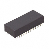
The device combines an internal
lithium battery, quartz crystal, clock
and power-fail chip, and a full
CMOS SRAM in a plastic 32-pin
DIP module. The RTC Module directly replaces industry-standard
SRAMs and also fits into many
EPR O M a n d E E P R O M s o ck e ts
without any requirement for special
write timing or limitations on the
number of write cycles.
Registers for the real-time clock,
alarm and other special functions
are located in registers 7FF0h–
7FFFh of the memory array.
The clock and alarm registers are
dual-port read/write SRAM locations that are updated once per second by a clock control circuit from
the internal clock counters. The
dual-port registers allow clock updates to occur without interrupting
normal access to the rest of the
SRAM array.
The bq4832Y also contains a powerfail-detect circuit. The circuit deselects the device whenever VCC falls
below tolerance, providing a high degree of data security. The battery is
electrically isolated when shipped
from the factory to provide maximum battery capacity. The battery
remains disconnected until the first
application of VCC.
➤ Software clock calibration for
greater than ± 1 minute per
month accuracy
Pin Names
Pin Connections
RST
NC
A14
A12
A7
A6
A5
A4
A3
A2
A1
A0
DQ0
DQ1
DQ2
VSS
1
2
3
4
5
6
7
8
9
10
11
12
13
14
15
16
32
31
30
29
28
27
26
25
24
23
22
21
20
19
18
17
VCC
NC
INT
WE
A13
A8
A9
A11
OE
A10
CE
DQ7
DQ6
DQ5
DQ4
DQ3
32-Pin DIP Module
PN483201.eps
Sept. 1996 C
1
A0–A14
Address input
CE
Chip enable
RST
Microprocessor reset
WE
Write enable
OE
Output enable
DQ0–DQ7
Data in/data out
INT
Programmable interrupt
VCC
+5 volts
VSS
Ground
�Not Recommended For New Designs Added
bq4832Y
including memory and clock interface, data-retention
modes, power-on reset timing, watchdog timer activation, and interrupt generation.
Functional Description
Figure 1 is a block diagram of the bq4832Y. The following sections describe the bq4832Y functional operation,
Figure 1. Block Diagram
Truth Table
VCC
CE
OE
WE
Mode
DQ
Power
< VCC (max.)
VIH
X
X
Deselect
High Z
Standby
VIL
X
VIL
Write
DIN
Active
VIL
VIL
VIH
Read
DOUT
Active
VIL
VIH
VIH
Read
High Z
Active
< VPFD (min.) > VSO
X
X
X
Deselect
High Z
CMOS standby
≤ VSO
X
X
X
Deselect
High Z
Battery-backup mode
> VCC (min.)
Sept. 1996 C
2
�Not Recommended For New Designs Added
bq4832Y
Address Map
CE and OE control the state of the eight three-state data
I/O signals. If the outputs are activated before tAA, the data
lines are driven to an indeterminate state until tAA. If the
address inputs are changed while CE and OE remain low,
output data remains valid for tOH (output data hold time),
but goes indeterminate until the next address access.
The bq4832Y provides 16 bytes of clock and control
status registers and 32,752 bytes of storage RAM.
Figure 2 illustrates the address map for the bq4832Y.
Table 1 is a map of the bq4832Y registers, and Table 2
describes the register bits.
Write Mode
Memory Interface
The bq4832Y is in write mode whenever WE and CE are
active. The start of a write is referenced from the
latter-occurring falling edge of WE or CE. A write is terminated by the earlier rising edge of WE or CE. The addresses must be held valid throughout the cycle. CE or
WE must return high for a minimum of tWR2 from CE
or tWR1 from WE prior to the initiation of another read
or write cycle.
Read Mode
The bq4832Y is in read mode whenever OE (output enable) is low and CE (chip enable) is low. The device architecture allows ripple-through access of data from
eight of 262,144 locations in the static storage array.
Thus, the unique address specified by the 15 address inputs defines which one of the 32,768 bytes of data is to
be accessed. Valid data is available at the data I/O pins
within tAA (address access time) after the last address
input signal is stable, providing that the CE and OE
(output enable) access times are also satisfied. If the CE
and OE access times are not met, valid data is available
after the latter of chip enable access time (tACE) or output enable access time (tOE).
16 Bytes
Clock and
Control Status
Registers
Data-in must be valid tDW prior to the end of write and
remain valid for tDH1 or tDH2 afterward. OE should be
kept high during write cycles to avoid bus contention; although, if the output bus has been activated by a low on
CE and OE, a low on WE disables the outputs tWZ after
WE falls.
7FFF
7FF0
7FEF
32,752
Bytes
7FFF
7FFE
7FFD
7FFC
7FFB
7FFA
7FF9
7FF8
7FF7
7FF6
7FF5
7FF4
7FF3
7FF2
14
Year
Month
Date
Days
Hours
Minutes
Seconds
Control
Watchdog
Interrupts
Alarm Date
Alarm Hours
Alarm Minutes
Alarm Seconds
Tenths/
Hundredths
15
Flags
7FF0
0
1
2
3
4
5
6
7
8
9
10
11
12
13
Storage
RAM
0000
7FF1
FG483201.eps
Figure 2. Address Map
Sept. 1996 C
3
�Not Recommended For New Designs Added
bq4832Y
Data-Retention Mode
Clock Interface
With valid VCC applied, the bq4832Y operates as a
conventional static RAM. Should the supply voltage
decay, the RAM automatically power-fail deselects,
write-protecting itself tWPT after VCC falls below VPFD.
All outputs become high impedance, and all inputs are
treated as “don’t care.”
Reading the Clock
The interface to the clock and control registers of the
bq4832Y is the same as that for the general-purpose
storage memory. Once every second, the user-accessible
clock/calendar locations are updated simultaneously
from the internal real time counters. To prevent reading
data in transition, updates to the bq4832Y clock registers should be halted. Updating is halted by setting the
read bit D6 of the control register to 1. As long as the
read bit is 1, updates to user-accessible clock locations
are inhibited. Once the frozen clock information is retrieved by reading the appropriate clock memory locations, the read bit should be reset to 0 in order to allow
updates to occur from the internal counters. Because the
internal counters are not halted by setting the read bit,
reading the clock locations has no effect on clock accuracy. Once the read bit is reset to 0, within one second
the internal registers update the user-accessible registers with the correct time. A halt command issued during a clock update allows the update to occur before
freezing the data.
If power-fail detection occurs during a valid access, the
memory cycle continues to completion. If the memory
cycle fails to terminate within time t WPT, writeprotection takes place. When VCC drops below VSO, the
control circuit switches power to the internal energy
source, which preserves data.
The internal coin cell maintains data in the bq4832Y after the initial application of VCC for an accumulated period of at least 10 years when VCC is less than VSO. As
system power returns and Vcc rises above VSO, the battery is disconnected, and the power supply is switched to
external VCC. Write-protection continues for tCER after
VCC reaches VPFD to allow for processor stabilization.
After tCER, normal RAM operation can resume.
Table 1. bq4832Y Clock and Control Register Map
Address
7FFF
7FFE
7FFD
7FFC
7FFB
7FFA
7FF9
7FF8
7FF7
7FF6
7FF5
7FF4
7FF3
7FF2
7FF1
7FF0
Notes:
D7
X
X
X
X
X
OSC
W
WDS
AIE
ALM3
ALM2
ALM1
ALM0
WDF
D6
D5
D4
10 Years
X
X
10 Month
X
10 Date
FTE
X
X
X
10 Hours
10 Minutes
10 Seconds
R
S
BM4
BM3
BM2
PWRIE ABE
PIE
X
10-date alarm
X
10-hour alarm
Alarm 10 minutes
Alarm 10 seconds
0.1 seconds
AF
PWRF
BLF
D3
D2
D1
Year
Month
Date
X
Day
Hours
Minutes
Seconds
Calibration
BM1
BM0
WD1
RS3
RS2
RS1
Alarm date
Alarm hours
Alarm minutes
Alarm seconds
0.01 seconds
PF
X
X
D0
Range (h)
00–99
01–12
01–31
01–07
00–23
00–59
00–59
00–31
WD0
RS0
01–31
00–23
00–59
00–59
00–99
X
Register
Year
Month
Date
Days
Hours
Minutes
Seconds
Control
Watchdog
Interrupts
Alarm date
Alarm hours
Alarm minutes
Alarm seconds
0.1/0.01 seconds
Flags
X = Unused bits; can be written and read.
Clock/Calendar data in 24-hour BCD format.
BLF = 1 for low battery.
OSC = 1 stops the clock oscillator.
Interrupt enables are cleared on power-up.
Sept. 1996 C
4
�Not Recommended For New Designs Added
bq4832Y
Calibrating the Clock
Table 2. Clock and Control Register Bits
Bits
The bq4832Y real-time clock is driven by a quartz controlled oscillator with a nominal frequency of 32,768 Hz.
The quartz crystal is contained within the bq4832Y
package along with the battery. The clock accuracy of
the bq4832Y module is tested to be within 20ppm or
about 1 minute per month at 25°C. The oscillation rates
of crystals change with temperature as Figure 3 shows.
To compensate for the frequency shift, the bq4832Y offers onboard software clock calibration. The user can
adjust the calibration based on the typical operating
temperature of individual applications.
Description
ABE
Alarm interrupt enable in
battery-backup mode
AF
Alarm interrupt flag
AIE
Alarm interrupt enable
ALM0–ALM3
Alarm repeat rate
BLF
Battery-low flag
BM0–BM4
Watchdog multiplier
FTE
Frequency test mode enable
OSC
Oscillator stop
PF
Periodic interrupt flag
PIE
Periodic interrupt enable
PWRF
Power-fail interrupt flag
PWRIE
Power-fail interrupt enable
R
Read clock enable
RS0–RS3
Periodic interrupt rate
S
Calibration sign
W
Write clock enable
WD0–WD1
Watchdog resolution
WDF
Watchdog flag
WDS
Watchdog steering
The software calibration bits are located in the control
register. Bits D0–D4 control the magnitude of correction, and bit D5 the direction (positive or negative) of
correction. Assuming that the oscillator is running at
exactly 32,786 Hz, each calibration step of D0–D4 adjusts the clock rate by +4.068 ppm (+10.7 seconds per
month) or -2.034 ppm (-5.35 seconds per month) depending on the value of the sign bit D5. When the sign bit is
1, positive adjustment occurs; a 0 activates negative adjustment. The total range of clock calibration is +5.5 or
-2.75 minutes per month.
Two methods can be used to ascertain how much calibration a given bq4832Y may require in a system. The
first involves simply setting the clock, letting it run for a
month, and then comparing the time to an accurate
known reference like WWV radio broadcasts. Based on
the variation to the standard, the end user can adjust
the clock to match the system’s environment even after
the product is packaged in a non-serviceable enclosure.
The only requirement is a utility that allows the end
user to access the calibration bits in the control register.
Setting the Clock
Bit D7 of the control register is the write bit. Like
the read bit, the write bit when set to a 1 halts updates to the clock/calendar memory locations. Once
frozen, the locations can be written with the desired
information in 24-hour BCD format. Resetting the
write bit to 0 causes the written values to be transferred to the internal clock counters and allows updates to the user-accessible registers to resume
within one second. Use the write bit, D7, only when
updating the time registers (7FFF-7FF9).
Stopping and Starting the Clock Oscillator
The OSC bit in the seconds register turns the clock
on or off. If the bq4832Y is to spend a significant period of time in storage, the clock oscillator can be
turned off to preserve battery capacity. OSC set to 1
stops the clock oscillator. When OSC is reset to 0,
the clock oscillator is turned on and clock updates to
user-accessible memory locations occur within one
second.
The OSC bit is set to 1 when shipped from the Benchmarq factory.
Figure 3. Frequency Error
Sept. 1996 C
5
�Not Recommended For New Designs Added
bq4832Y
ally, when the watchdog times out, the watchdog flag bit
(WDF) in the flags register, location 7FF0, is set.
The second approach uses a bq4832Y test mode. When
the frequency test mode enable bit FTE in the days register is set to a 1, and the oscillator is running at exactly
32,768 Hz, the LSB of the seconds register toggles at 512
Hz. Any deviation from 512 Hz indicates the degree and
direction of oscillator frequency shift at the test temperature. For example, a reading of 512.01024 Hz indicates a (1E6*0.01024)/512 or +20 ppm oscillator frequency error, requiring ten steps of negative calibration
(10*-2.034 or -20.34) or 001010 to be loaded into the calibration byte for correction. To read the test frequency,
the bq4832Y must be selected and held in an extended
read of the seconds register, location 7FF9, without having the read bit set. The frequency appears on DQ0.
The FTE bit must be set using the write bit control. The
FTE bit must be reset to 0 for normal clock operation to
resume.
To reset the watchdog timer, the microprocessor must
write to the watchdog register. After being reset by a
write, the watchdog time-out period starts over. As a
precaution, the watchdog circuit is disabled on a power
failure. The user must, therefore, set the watchdog at
boot-up for activation.
Interrupts
The bq4832Y allows four individually selected interrupt
events to generate an interrupt request on the INT pin.
These four interrupt events are:
n The watchdog timer interrupt, programmable to
occur according to the time-out period and conditions
described in the watchdog timer section.
Power-On Reset
n The periodic interrupt, programmable to occur once
every 122µs to 500ms.
The bq4832Y provides a power-on reset, which pulls the
RST pin low on power-down and remains low on powerup for tCER after VCC passes VPFD.
n The alarm interrupt, programmable to occur once per
second to once per month.
Watchdog Timer
n The power-fail interrupt, which can be enabled to be
asserted when the bq4832Y detects a power failure.
The watchdog circuit monitors the microprocessor’s activity. If the processor does not reset the watchdog timer
within the programmed time-out period, the circuit asserts the INT or RST pin. The watchdog timer is activated by writing the desired time-out period into the
eight-bit watchdog register described in Table 3 (device
address 7FF7). The five bits (BM4–BM0) store a binary
multiplier, and the two lower-order bits (WD1–WD0) select the resolution, where 00 = 1 16 second, 01 = 1 4 second,
10 = 1 second, and 11 = 4 seconds.
The periodic, alarm, and power-fail interrupts are enabled by an individual interrupt-enable bit in register
7FF6, the interrupts register. When an event occurs, its
event flag bit in the flags register, location 7FF0, is set.
If the corresponding event enable bit is also set, then an
interrupt request is generated. Reading the flags register clears all flag bits and makes INT high impedance.
To reset the flag register, the bq4832Y addresses must
be held stable at location 7FF0 for at least 50ns to avoid
inadvertent resets.
The time-out period is the multiplication of the five-bit
multiplier with the two-bit resolution. For example,
writing 00011 in BM4–BM0 and 10 in WD1–WD0 results in a total time-out setting of 3 x 1 or 3 seconds. A
multiplier of zero disables the watchdog circuit. Bit 7 of
the watchdog register (WDS) is the watchdog steering
bit. When WDS is set to a 1 and a time-out occurs, the
watchdog asserts a reset pulse for tCER on the RST pin.
During the reset pulse, the watchdog register is cleared
to all zeros disabling the watchdog. When WDS is set to
a 0, the watchdog asserts the INT pin on a time-out.
The INT pin remains low until the watchdog is reset by
the microprocessor or a power failure occurs. Addition-
Periodic Interrupt
Bits RS3–RS0 in the interrupts register program the
rate for the periodic interrupt. The user can interpret
the interrupt in two ways: either by polling the flags
register for PF assertion or by setting PIE so that INT
goes active when the bq4832Y sets the periodic flag.
Reading the flags register resets the PF bit and returns INT to the high-impedance state. Table 4 shows
the periodic rates.
Table 3. Watchdog Register Bits
MSB
Bits
LSB
7
6
5
4
3
2
1
WDS
BM4
BM3
BM2
BM1
BM0
WD1
0
WD0
Sept. 1996 C
6
�Not Recommended For New Designs Added
bq4832Y
Table 5. Alarm Frequency
(Alarm Bits DQ7 of Alarm Registers)
Table 4. Periodic Rates
RS3
RS2
RS1
RS0
Interrupt
Rate
ALM3
ALM2
ALM1
ALM0
1
1
1
1
Once per second
Alarm Frequency
1
1
1
0
Once per minute
when seconds match
1
1
0
0
Once per hour when
minutes, and seconds
match
1
0
0
0
Once per day when
hours, minutes, and
seconds match
0
0
0
0
When date, hours,
minutes, and seconds
match
0
0
0
0
None
0
0
0
1
10ms
0
0
1
0
100ms
0
0
1
1
122.07µs
0
1
0
0
244.14µs
0
1
0
1
488.281µs
0
1
1
0
976.5625
0
1
1
1
1.953125ms
1
0
0
0
3.90625ms
1
0
0
1
7.8125ms
1
0
1
0
15.625ms
1
0
1
1
31.25ms
1
1
0
0
62.5ms
1
1
0
1
125ms
1
1
1
0
250ms
Power-Fail Interrupt
1
1
1
1
500ms
When V CC falls to the power-fail-detect point, the
power-fail flag PWRF is set. If the power-fail interrupt
enable bit (PWRIE) is also set, then INT is asserted low.
The power-fail interrupt occurs tWPT before the bq4832Y
generates a reset and deselects. The PWRIE bit is
cleared on power-up.
The alarm interrupt can be made active while the
bq4832Y is in the battery-backup mode by setting ABE
in the interrupts register. Normally, the INT pin tristates during battery backup. With ABE set, however,
INT is driven low if an alarm condition occurs and the
AIE bit is set. Because the AIE bit is reset during
power-on reset, an alarm generated during power-on reset updates only the flags register. The user can read
the flags register during boot-up to determine if an
alarm was generated during power-on reset.
Alarm Interrupt
Registers 7FF5–7FF2 program the real-time clock
alarm. During each update cycle, the bq4832Y compares
the date, hours, minutes, and seconds in the clock registers with the corresponding alarm registers. If a match
between all the corresponding bytes is found, the alarm
flag AF in the flags register is set. If the alarm interrupt is enabled with AIE, an interrupt request is generated on INT. The alarm condition is cleared by a read to
the flags register. ALM3–ALM0 puts the alarm into a periodic mode of operation. Table 5 describes the selectable
rates.
Battery-Low Warning
The bq4832Y checks the internal battery on power-up.
If the battery voltage is below 2.2V, the battery-low flag
BLF in the flags register is set to a 1 indicating that
clock and RAM data may be invalid.
Sept. 1996 C
7
�Not Recommended For New Designs Added
bq4832Y
Absolute Maximum Ratings
Symbol
Parameter
Value
Unit
VCC
DC voltage applied on VCC relative to VSS
-0.3 to 7.0
V
VT
DC voltage applied on any pin excluding VCC
relative to VSS
-0.3 to 7.0
V
TOPR
Operating temperature
0 to +70
°C
TSTG
Storage temperature (VCC off; oscillator off)
-40 to +70
°C
TBIAS
Temperature under bias
-10 to +70
°C
TSOLDER
Soldering temperature
+260
°C
Note:
Conditions
VT ≤ VCC + 0.3
For 10 seconds
Permanent device damage may occur if Absolute Maximum Ratings are exceeded. Functional operation
should be limited to the Recommended DC Operating Conditions detailed in this data sheet. Exposure to conditions beyond the operational limits for extended periods of time may affect device reliability.
Recommended DC Operating Conditions (TA = TOPR)
Symbol
Note:
Parameter
Minimum
Typical
Maximum
Unit
VCC
Supply voltage
4.5
5.0
5.5
V
VSS
Supply voltage
0
0
0
V
VIL
Input low voltage
-0.3
-
0.8
V
VIH
Input high voltage
2.2
-
VCC + 0.3
V
Notes
Typical values indicate operation at TA = 25°C.
Sept. 1996 C
8
�Not Recommended For New Designs Added
bq4832Y
DC Electrical Characteristics (TA = TOPR, VCCmin
Symbol
Parameter
≤ VCC ≤ VCCmax)
Minimum
Typical
Maximum
Unit
Conditions/Notes
ILI
Input leakage current
-
-
±1
µA
VIN = VSS to VCC
ILO
Output leakage current
-
-
±1
µA
CE = VIH or OE = VIH or
WE = VIL
VOH
Output high voltage
2.4
-
-
V
IOH = -1.0 mA
VOL
Output low voltage
-
-
0.4
V
IOL = 2.1 mA
IOD
RST, INT sink current
10
-
-
mA
VOL = 0.4V
ISB1
Standby supply current
-
3
6
mA
CE = VIH
ISB2
Standby supply current
-
2
4
mA
CE ≥ VCC - 0.2V,
0V ≤ VIN ≤ 0.2V,
or VIN ≥ VCC - 0.2V
ICC
Operating supply current
-
55
75
mA
Min. cycle, duty = 100%,
CE = VIL, II/O = 0mA
VPFD
Power-fail-detect voltage
4.30
4.37
4.50
V
VSO
Supply switch-over voltage
-
3
-
V
Notes:
Typical values indicate operation at TA = 25°C, VCC = 5V.
RST and INT are open-drain outputs.
Capacitance (TA = 25°C, F = 1MHz, VCC = 5.0V)
Symbol
Parameter
Minimum
Typical
Maximum
Unit
Conditions
CI/O
Input/output capacitance
-
-
10
pF
Output voltage = 0V
CIN
Input capacitance
-
-
10
pF
Input voltage = 0V
Note:
These parameters are sampled and not 100% tested.
Sept. 1996 C
9
�Not Recommended For New Designs Added
bq4832Y
AC Test Conditions
Parameter
Test Conditions
Input pulse levels
0V to 3.0V
Input rise and fall times
5 ns
Input and output timing reference levels
1.5 V (unless otherwise specified)
Output load (including scope and jig)
See Figures 4 and 5
Figure 4. Output Load A
Read Cycle
Figure 5. Output Load B
(TA = TOPR, VCCmin ≤ VCC ≤ VCCmax)
–85
Symbol
Parameter
Min.
Max.
Unit
85
-
ns
Conditions
tRC
Read cycle time
tAA
Address access time
-
85
ns
Output load A
tACE
Chip enable access time
-
85
ns
Output load A
tOE
Output enable to output valid
-
45
ns
Output load A
tCLZ
Chip enable to output in low Z
5
-
ns
Output load B
tOLZ
Output enable to output in low Z
0
-
ns
Output load B
tCHZ
Chip disable to output in high Z
0
35
ns
Output load B
tOHZ
Output disable to output in high Z
0
25
ns
Output load B
tOH
Output hold from address change
10
-
ns
Output load A
Sept. 1996 C
10
�Not Recommended For New Designs Added
bq4832Y
Read Cycle No. 1 (Address Access) 1,2
Read Cycle No. 2 (CE Access) 1,3,4
Read Cycle No. 3 (OE Access) 1,5
Notes:
1. WE is held high for a read cycle.
2. Device is continuously selected: CE = OE = VIL.
3. Address is valid prior to or coincident with CE transition low.
4. OE = VIL.
5. Device is continuously selected: CE = VIL.
Sept. 1996 C
11
�Not Recommended For New Designs Added
bq4832Y
Write Cycle
(TA =TOPR , VCCmin ≤ VCC ≤ VCCmax)
–85
Symbol
Parameter
Min.
Max.
Units
Conditions/Notes
tWC
Write cycle time
85
-
ns
tCW
Chip enable to end of write
75
-
ns
(1)
tAW
Address valid to end of write
75
-
ns
(1)
tAS
Address setup time
0
-
ns
Measured from address valid to beginning of write. (2)
tWP
Write pulse width
65
-
ns
Measured from beginning of write to
end of write. (1)
tWR1
Write recovery time (write cycle 1)
5
-
ns
Measured from WE going high to end of
write cycle. (3)
tWR2
Write recovery time (write cycle 2)
15
-
ns
Measured from CE going high to end of
write cycle. (3)
tDW
Data valid to end of write
35
-
ns
Measured to first low-to-high transition
of either CE or WE.
tDH1
Data hold time (write cycle 1)
0
-
ns
Measured from WE going high to end of
write cycle. (4)
tDH2
Data hold time (write cycle 2)
10
-
ns
Measured from CE going high to end of
write cycle. (4)
tWZ
Write enabled to output in high Z
0
30
ns
I/O pins are in output state. (5)
tOW
Output active from end of write
0
-
ns
I/O pins are in output state. (5)
Notes:
1. A write ends at the earlier transition of CE going high and WE going high.
2. A write occurs during the overlap of a low CE and a low WE. A write begins at the later transition
of CE going low and WE going low.
3. Either tWR1 or tWR2 must be met.
4. Either tDH1 or tDH2 must be met.
5. If CE goes low simultaneously with WE going low or after WE going low, the outputs remain in
high-impedance state.
Sept. 1996 C
12
�Not Recommended For New Designs Added
bq4832Y
Write Cycle No. 1 (WE-Controlled) 1,2,3
Write Cycle No. 2 (CE-Controlled) 1,2,3,4,5
Notes:
1. CE or WE must be high during address transition.
2. Because I/O may be active (OE low) during this period, data input signals of opposite polarity to the
outputs must not be applied.
3. If OE is high, the I/O pins remain in a state of high impedance.
4. Either tWR1 or tWR2 must be met.
5. Either tDH1 or tDH2 must be met.
Sept. 1996 C
13
�Not Recommended For New Designs Added
bq4832Y
Power-Down/Power-Up Cycle (TA = TOPR)
Minimum
Typical
Maximum
Unit
tPF
Symbol
VCC slew, 4.50 to 4.20 V
300
-
-
µs
tFS
VCC slew, 4.20 to VSO
10
-
-
µs
tPU
VCC slew, VSO to VPFD
(max.)
0
-
-
µs
tCER
Chip enable recovery time
40
100
200
ms
tDR
Data-retention time in
absence of VCC
10
-
-
years
tWPT
Write-protect time
40
100
160
µs
Notes:
Parameter
Conditions
Time during which SRAM is
write-protected after VCC
passes VFPD on power-up.
TA = 25°C. (2)
Delay after VCC slews down
past VPFD before SRAM is
write-protected.
1. Typical values indicate operation at TA = 25°C, VCC = 5V.
2. Battery is disconnected from circuit until after VCC is applied for the first time. tDR is the
accumulated time in absence of power beginning when power is first applied to the device.
Caution: Negative undershoots below the absolute maximum rating of -0.3V in battery-backup mode
may affect data integrity.
Power-Down/Power-Up Timing
Notes:
1. PWRIE is set to “1” to enable power fail interrupt.
2. RST and INT are open drain and require an external pull-up resistor.
Sept. 1996 C
14
�Not Recommended For New Designs Added
bq4832Y
Data Sheet Revision History
Change No.
Page No.
1
4
Corrected the locations of bits D6 and D4 of the Interrupts Register and the corresponding bits D5 and D3 of the Flags Register (these were reversed).
2
4
Corrected the alarm date register (7FF5) to allow for 01-31 days in a month instead
of 01-07 days.
2
9
Lowered ISB1 from 4, 7mA to 3, 6mA; lowered ISB2 typical from 2.5mA to 2mA.
Notes:
Description
Change 1 = Mar. 1996 B changes from Oct. 1995 A.
Change 2 = Sept. 1996 C changes from Mar. 1996 B.
Sept. 1996 C
15
�Not Recommended For New Designs Added
bq4832Y
MA: 32-Pin A-Type Module
32-Pin MA (A-Type Module)
Inches
Millimeters
Dimension
Min.
Max.
Min.
Max.
A
0.365
0.375
9.27
9.53
A1
0.015
-
0.38
-
B
0.017
0.023
0.43
0.58
C
0.008
0.013
0.20
0.33
D
1.670
1.700
42.42
43.18
E
0.710
0.740
18.03
18.80
e
0.590
0.630
14.99
16.00
G
0.090
0.110
2.29
2.79
L
0.120
0.150
3.05
3.81
S
0.075
0.110
1.91
2.79
Sept. 1996 C
16
�Not Recommended For New Designs Added
bq4832Y
Ordering Information
bq4832Y MA Speed Options:
85 = 85 ns
Package Option:
MA = A-type module
Device:
bq4832Y 32K x 8 Real-Time Clock Module
Sept. 1996 C
17
�PACKAGE OPTION ADDENDUM
www.ti.com
6-Nov-2014
PACKAGING INFORMATION
Orderable Device
Status
(1)
BQ4832YMA-85
Package Type Package Pins Package
Drawing
Qty
OBSOLETE DIP MODULE
MA
32
Eco Plan
Lead/Ball Finish
MSL Peak Temp
(2)
(6)
(3)
TBD
Call TI
Call TI
Op Temp (°C)
Device Marking
(4/5)
0 to 70
(1)
The marketing status values are defined as follows:
ACTIVE: Product device recommended for new designs.
LIFEBUY: TI has announced that the device will be discontinued, and a lifetime-buy period is in effect.
NRND: Not recommended for new designs. Device is in production to support existing customers, but TI does not recommend using this part in a new design.
PREVIEW: Device has been announced but is not in production. Samples may or may not be available.
OBSOLETE: TI has discontinued the production of the device.
(2)
Eco Plan - The planned eco-friendly classification: Pb-Free (RoHS), Pb-Free (RoHS Exempt), or Green (RoHS & no Sb/Br) - please check http://www.ti.com/productcontent for the latest availability
information and additional product content details.
TBD: The Pb-Free/Green conversion plan has not been defined.
Pb-Free (RoHS): TI's terms "Lead-Free" or "Pb-Free" mean semiconductor products that are compatible with the current RoHS requirements for all 6 substances, including the requirement that
lead not exceed 0.1% by weight in homogeneous materials. Where designed to be soldered at high temperatures, TI Pb-Free products are suitable for use in specified lead-free processes.
Pb-Free (RoHS Exempt): This component has a RoHS exemption for either 1) lead-based flip-chip solder bumps used between the die and package, or 2) lead-based die adhesive used between
the die and leadframe. The component is otherwise considered Pb-Free (RoHS compatible) as defined above.
Green (RoHS & no Sb/Br): TI defines "Green" to mean Pb-Free (RoHS compatible), and free of Bromine (Br) and Antimony (Sb) based flame retardants (Br or Sb do not exceed 0.1% by weight
in homogeneous material)
(3)
MSL, Peak Temp. - The Moisture Sensitivity Level rating according to the JEDEC industry standard classifications, and peak solder temperature.
(4)
There may be additional marking, which relates to the logo, the lot trace code information, or the environmental category on the device.
(5)
Multiple Device Markings will be inside parentheses. Only one Device Marking contained in parentheses and separated by a "~" will appear on a device. If a line is indented then it is a continuation
of the previous line and the two combined represent the entire Device Marking for that device.
(6)
Lead/Ball Finish - Orderable Devices may have multiple material finish options. Finish options are separated by a vertical ruled line. Lead/Ball Finish values may wrap to two lines if the finish
value exceeds the maximum column width.
Important Information and Disclaimer:The information provided on this page represents TI's knowledge and belief as of the date that it is provided. TI bases its knowledge and belief on information
provided by third parties, and makes no representation or warranty as to the accuracy of such information. Efforts are underway to better integrate information from third parties. TI has taken and
continues to take reasonable steps to provide representative and accurate information but may not have conducted destructive testing or chemical analysis on incoming materials and chemicals.
TI and TI suppliers consider certain information to be proprietary, and thus CAS numbers and other limited information may not be available for release.
In no event shall TI's liability arising out of such information exceed the total purchase price of the TI part(s) at issue in this document sold by TI to Customer on an annual basis.
Addendum-Page 1
Samples
�IMPORTANT NOTICE
Texas Instruments Incorporated and its subsidiaries (TI) reserve the right to make corrections, enhancements, improvements and other
changes to its semiconductor products and services per JESD46, latest issue, and to discontinue any product or service per JESD48, latest
issue. Buyers should obtain the latest relevant information before placing orders and should verify that such information is current and
complete. All semiconductor products (also referred to herein as “components”) are sold subject to TI’s terms and conditions of sale
supplied at the time of order acknowledgment.
TI warrants performance of its components to the specifications applicable at the time of sale, in accordance with the warranty in TI’s terms
and conditions of sale of semiconductor products. Testing and other quality control techniques are used to the extent TI deems necessary
to support this warranty. Except where mandated by applicable law, testing of all parameters of each component is not necessarily
performed.
TI assumes no liability for applications assistance or the design of Buyers’ products. Buyers are responsible for their products and
applications using TI components. To minimize the risks associated with Buyers’ products and applications, Buyers should provide
adequate design and operating safeguards.
TI does not warrant or represent that any license, either express or implied, is granted under any patent right, copyright, mask work right, or
other intellectual property right relating to any combination, machine, or process in which TI components or services are used. Information
published by TI regarding third-party products or services does not constitute a license to use such products or services or a warranty or
endorsement thereof. Use of such information may require a license from a third party under the patents or other intellectual property of the
third party, or a license from TI under the patents or other intellectual property of TI.
Reproduction of significant portions of TI information in TI data books or data sheets is permissible only if reproduction is without alteration
and is accompanied by all associated warranties, conditions, limitations, and notices. TI is not responsible or liable for such altered
documentation. Information of third parties may be subject to additional restrictions.
Resale of TI components or services with statements different from or beyond the parameters stated by TI for that component or service
voids all express and any implied warranties for the associated TI component or service and is an unfair and deceptive business practice.
TI is not responsible or liable for any such statements.
Buyer acknowledges and agrees that it is solely responsible for compliance with all legal, regulatory and safety-related requirements
concerning its products, and any use of TI components in its applications, notwithstanding any applications-related information or support
that may be provided by TI. Buyer represents and agrees that it has all the necessary expertise to create and implement safeguards which
anticipate dangerous consequences of failures, monitor failures and their consequences, lessen the likelihood of failures that might cause
harm and take appropriate remedial actions. Buyer will fully indemnify TI and its representatives against any damages arising out of the use
of any TI components in safety-critical applications.
In some cases, TI components may be promoted specifically to facilitate safety-related applications. With such components, TI’s goal is to
help enable customers to design and create their own end-product solutions that meet applicable functional safety standards and
requirements. Nonetheless, such components are subject to these terms.
No TI components are authorized for use in FDA Class III (or similar life-critical medical equipment) unless authorized officers of the parties
have executed a special agreement specifically governing such use.
Only those TI components which TI has specifically designated as military grade or “enhanced plastic” are designed and intended for use in
military/aerospace applications or environments. Buyer acknowledges and agrees that any military or aerospace use of TI components
which have not been so designated is solely at the Buyer's risk, and that Buyer is solely responsible for compliance with all legal and
regulatory requirements in connection with such use.
TI has specifically designated certain components as meeting ISO/TS16949 requirements, mainly for automotive use. In any case of use of
non-designated products, TI will not be responsible for any failure to meet ISO/TS16949.
Products
Applications
Audio
www.ti.com/audio
Automotive and Transportation
www.ti.com/automotive
Amplifiers
amplifier.ti.com
Communications and Telecom
www.ti.com/communications
Data Converters
dataconverter.ti.com
Computers and Peripherals
www.ti.com/computers
DLP® Products
www.dlp.com
Consumer Electronics
www.ti.com/consumer-apps
DSP
dsp.ti.com
Energy and Lighting
www.ti.com/energy
Clocks and Timers
www.ti.com/clocks
Industrial
www.ti.com/industrial
Interface
interface.ti.com
Medical
www.ti.com/medical
Logic
logic.ti.com
Security
www.ti.com/security
Power Mgmt
power.ti.com
Space, Avionics and Defense
www.ti.com/space-avionics-defense
Microcontrollers
microcontroller.ti.com
Video and Imaging
www.ti.com/video
RFID
www.ti-rfid.com
OMAP Applications Processors
www.ti.com/omap
TI E2E Community
e2e.ti.com
Wireless Connectivity
www.ti.com/wirelessconnectivity
Mailing Address: Texas Instruments, Post Office Box 655303, Dallas, Texas 75265
Copyright © 2014, Texas Instruments Incorporated
�


 工商网监
湘ICP备2023018690号
工商网监
湘ICP备2023018690号
