Not Recommended for New Designs
bq6400
www.ti.com ......................................................................................................................................................................................... SLUS841 – SEPTEMBER 2008
Single Chip 3 or 4 Cell Li-Ion Battery Management Controller With PowerPump™ Cell
Balancing Technology
FEATURES
1
• Advanced SmartSafety™
– Prevention – Optimal Cell Management
– Diagnosis – Improved Sensing of Cell
Problems
– Fail Safe – Detection of Event Precursors
• Rate-of-Change Detection of all Important Cell
Characteristics:
– Voltage – Impedance – Cell Temperature
• PowerPump™ Active Cell Balancing Results in
Longer Run Time and Cell Life
• High Resolution 18-Bit Integrating Delta-Sigma
Coulomb Counter for Precise Charge-Flow
Measurements and Gas Gauging
• Multiple Independent Δ-Σ A/Ds: One-per-cell
Voltage, Plus Separate Temperature, Current
and Safety
• Simultaneous, Synchronous Measurement of
Pack Current and Individual Cell Voltages
• Very Low Power Consumption: < 250 µA
Active, < 150 µA Standby, < 40 µA Ship, and <
1 A Under-Voltage Shutdown
• Accurate, Advanced Temperature Monitoring
of Cells and MOSFETs With up to 13 Sensors
• Fully Programmable Voltage, Current, Balance
and Temperature Protection Features
• Cell Balancing Transfers Charge Efficiently
From Cell to Cell During all Operating
Conditions
• Fail-Safe Operation of Pack Protection Circuits
and MOSFETs
• Designed for 3 to 4 Series Cell Battery Packs
• Smart Battery System 1.1 Compliant
• Integrated Support for Intel™ AMPS
• Field Upgradeable Flash Memory
23
APPLICATIONS
•
•
•
Notebook Computer Battery Packs
Portable Medical Equipment
Portable Test Equipment
DESCRIPTION
The bq6400 Battery Management Controller is a
complete Li-Ion control, monitoring, and safety
solution designed for notebook computers and
portable equipment. It is designed specifically to
provide an enhanced, optimized solution for packs
using three or four series cells.
The bq6400 provides accurate gas gauging while
providing control, communications and safety
functions for the system. It provides simultaneous,
synchronized voltage and temperature measurements
using one A/D per-cell technology. Voltage
measurements are also simultaneous with pack
current measurements, eliminating system induced
noise from measurements. This allows the precise,
continuous, real-time calculation of cell impedance
under all operating conditions, even during widely
fluctuating loads.
PowerPump™ technology transfers charge between
cells to balance their voltage and capacity. Balancing
is programmable during all battery modes: Charge,
discharge, and rest. Highly efficient charge transfer
circuitry nearly eliminates energy loss while providing
true real-time balance between cells, resulting in
longer run-time and improved cell cycle life.
Temperature is sensed by one internal and up to 12
external sensors. This permits accurate temperature
monitoring of each cell individually as well as pack
protection MOSFETs. Internal firmware is then able to
compensate for the temperature induced effects on
cell capacity, impedance, and OCV on a cell-by-cell
basis, resulting in superior charge/discharge and
balancing control.
Support for Intel™ Adaptive Mobile Power System
(AMPS) requirements for battery and MOSFET
control is built-in. User definable inputs require no
external hardware translation logic.
The bq6400 is completely user-configurable with
parametric tables in flash memory to suit a variety of
cell chemistries, operating conditions, safety control,
and data reporting needs. It is easily configured using
the supplied Battery Wizard™ graphical user
interface. The device is fully programmed and
requires no algorithm or firmware development.
1
2
3
Please be aware that an important notice concerning availability, standard warranty, and use in critical applications of Texas
Instruments semiconductor products and disclaimers thereto appears at the end of this data sheet.
PowerPump, SmartSafety are trademarks of Texas Instruments.
Intel is a trademark of Intel Corporation.
PRODUCTION DATA information is current as of publication date.
Products conform to specifications per the terms of the Texas
Instruments standard warranty. Production processing does not
necessarily include testing of all parameters.
Copyright © 2008, Texas Instruments Incorporated
�Not Recommended for New Designs
bq6400
SLUS841 – SEPTEMBER 2008 ......................................................................................................................................................................................... www.ti.com
These devices have limited built-in ESD protection. The leads should be shorted together or the device placed in conductive foam
during storage or handling to prevent electrostatic damage to the MOS gates.
Voltage
Balance
Temp
V1
PUMP 1
XT1*
Voltage
Balance
Temp
1 Level Safety
& FET Control
FLASH
CELL 3
V2
PUMP 2
XT2*
EFCIC
8 bit
RISC
CPU
Coulomb Counter
CCBAT
CCPACK
Current A /D
Internal
Oscillator
LED Control
6
Reset
Logic
RSTN
I/O
Safety
LED1-5,
LEDEN
SMBCLK
SMBDAT
SMBus
Watchdog
Measure
FUSE
CSBAT
CSPACK
2 nd Level
Safety
Internal
Temperature
Core / CPU
PRE
CHG
DSG
EFCID
st
SRAM
Voltage
Balance
Temp
2.5V LDO-2
CELL 4
V3
PUMP 3
XT 3
2.5V LDO-1
Voltage
Balance
Temp
CELL 1
V4
PUMP 4
XT 4
CELL 2
bq6400 BLOCK DIAGRAM
ALERT
Pack Interface
* XT1 & XT2 inputs can optionally multiplex up
to five (5) additional temperature sensors each
.
AVAILABLE OPTIONS (1)
(1)
2
PRODUCT
PACKAGE
PACKAGE
DESIGNATOR
SPECIFIED
TEMPERATURE
RANGE
ORDERING
NUMBER
TRANSPORT MEDIA
QUANTITY
bq6400
QFN-48 7×7mm
RGZ
–40°C to 85°C
bq6400RGZR
Reel
For the most current package and ordering information, see the Package Option Addendum at the end of this document, or see the TI
website at www.ti.com.
Submit Documentation Feedback
Copyright © 2008, Texas Instruments Incorporated
Product Folder Link(s) :bq6400
�Not Recommended for New Designs
bq6400
www.ti.com ......................................................................................................................................................................................... SLUS841 – SEPTEMBER 2008
XT4
V4
SMBDAT
SMBCLK
40
39
38
37
V3
XT3
42
41
V2
VLDO2
44
43
XT1
XT2
46
45
VSS
V1
48
47
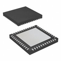
QFN-48 PACKAGE
CHG
1
36
LED 5
DSG
2
35
LED 4
PRE
3
34
LED 3
EFCIC
4
33
LED 2
EFCID
5
32
LED 1
CCBAT
6
31
LEDEN
CCPACK
7
30
FUSE
VLDO1
8
29
XC
CSBAT
9
28
MISO/ALERT
CSPACK
10
27
MOSI
NC
11
26
SCLK
NC
12
25
RSTN
24
23
P4N
NC
21
22
P4S
P3N
19
20
P3S
SDI3
18
17
P2N
16
13
15
P1N
P2S
SDO2
*
SDI1
49
B
TA
SDO0
14
bq6400
*Tab connection located bottom
center
, see mechanical drawing
for detail
.
TERMINAL FUNCTIONS
TERMINAL
NO.
(1)
NAME
I/O (1)
DESCRIPTION
1
CHG
O
Charge MOSFET control (Active high, enables current flow.)
2
DSG
O
Discharge MOSFET Control (Active high. Low opens MOSFET.)
3
PRE
O
Pre-Charge MOSFET control (Active high.)
4
EFCIC
I
External Charge FET Control, Intel™ AMPS compatible input
5
EFCID
I
6
CCBAT
IA
Coulomb counter input (sense resistor), connect to battery negative
7
CCPACK
IA
Coulomb counter input (sense resistor), connect to pack negative
8
VLDO1
P
Internal LDO-1 output, bypass with capacitor
External Discharge FET Control, Intel™AMPS compatible input
9
CSBAT
IA
Current sense input (safety), connect to battery negative
10
CSPACK
IA
Current sense input (safety), connect to pack negative
11
N/C
–
Do not connect to this pin
12
N/C
–
Do not connect to this pin
13
SDO0
O
Requires 100kΩ pull-up resistor to VLDO1
14
SDI1
I
Connect to SDO0 via a capacitor
15
P1N
O
Charge balance gate drive, cell 1 North
16
P2S
O
Charge balance gate drive, cell 2 South
17
P2N
O
Charge balance gate drive, cell 2 North
18
SDO2
O
Connect to SDI3 via capacitor
19
SDI3
I
Connect to SDO2 via capacitor
20
P3S
O
Charge balance gate drive, cell 3 South
21
P3N
O
Charge balance gate drive, cell 3 North
22
P4S
O
Charge balance gate drive, cell 4 South
23
P4N
O
Charge balance gate drive, cell 4 North
24
N/C
–
Do not connect to this pin
25
RSTN
I
Device reset, active low
I – input, IA – analog input, O – output, OA – analog output, OD – open drain output, p – power
Submit Documentation Feedback
Copyright © 2008, Texas Instruments Incorporated
Product Folder Link(s) :bq6400
3
�Not Recommended for New Designs
bq6400
SLUS841 – SEPTEMBER 2008 ......................................................................................................................................................................................... www.ti.com
TERMINAL FUNCTIONS (continued)
TERMINAL
NO.
4
NAME
I/O (1)
DESCRIPTION
26
SCLK
–
Do not connect to this pin
27
MOSI
I
Do not connect to this pin
28
MISO/ALERT
O
Optional ALERT output – asserted low on alarm condition (interrupt)
29
XC
O
Aux control
30
FUSE
O
Safety fuse control output, active high
31
LEDEN
O
LED common anode drive (hi), Aux Temp(n) input enable (low)
32
LED1
IO
SOCi LED drive (active low), Aux Temp input
33
LED2
IO
SOCi LED drive (active low), Aux Temp input
34
LED3
IO
SOCi LED drive (active low), Aux Temp input
35
LED4
IO
SOCi LED drive (active low), Aux Temp input
36
LED5
IO
SOCi LED drive (active low), Aux Temp input
37
SMBCLK
IO
SMBus clock signal
38
SMBDAT
IO
SMBus data signal
39
V4
IA
Cell 4 positive input
40
XT4
IA
External temperature sensor 4 input
41
XT3
IA
External temperature sensor 3 input
42
V3
IA
Cell 3 positive input
43
VLDO2
P
Internal LDO-2 output, bypass with capacitor
44
V2
IA
Cell 2 positive input
45
XT2
IA
External temperature sensor 2 input / mux temp input 2
46
XT1
IA
External temperature sensor 1 input / mux temp input 1
47
V1
IA
Cell 1 positive input
48
VSS
IA
Cell 1 negative input
TAB
TAB
P
Connect to VSS
Submit Documentation Feedback
Copyright © 2008, Texas Instruments Incorporated
Product Folder Link(s) :bq6400
�Not Recommended for New Designs
bq6400
www.ti.com ......................................................................................................................................................................................... SLUS841 – SEPTEMBER 2008
ABSOLUTE MAXIMUM RATINGS (1)
over operating free-air temperature range (unless otherwise noted)
RANGE
UNITS
TA
Operating free-air temperature (ambient)
–40 to 85
°C
TSTORAGE
Storage temperature
–65 to 150
°C
V4-V3
Max cell voltage
–0.5 to 5.0
V
V3-V2
Max cell voltage
–0.5 to 5.0
V
V2-V1
Max cell voltage
–0.5 to 5.0
V
V1-VSS
Max cell voltage
–0.5 to 5.0
V
Voltage on LED1-5
With respect to VSS
0.5 to 5.0
V
V
Voltage on CCBAT, CCPACK, CSBAT, CSPACK,
XT1, XT2,SDIX, SDOX, LEDEN, FUSE
Max voltage on any I/O pin
(VSS – 0.5) to
(VLDO1 + 0.5)
Voltage on XT3, XT4
Maximum voltage range
(V2 – 0.5) to
(VLDO2 + 0.5)
V
EFCIC, EFCID
With respect to VSS
–0.5 to 5.5
V
Voltage on SMBCLK, SMBDAT, ALERT
With respect to VSS
–0.5 to 6.0V
V
Voltage on PRE, CHG, DSG
With respect to VSS
–0.5 to (VLDO1 + 0.5)
V
Current through PRE, CHG, DSG, LEDEN, LED1-5 Maximum current source/sink
20
mA
VLDO1 maximum current
Maximum current draw from VLDO
20
mA
ESD tolerance
JEDEC, JESD22-A114 Human Body Model,
R=1500 Ω, C=100 pF
2
kV
Lead Temperature Soldering
Total time < 3 seconds
< 300
°C
(1)
Stresses or conditions in excess of those listed may cause permanent damage to the device. Exposure to these conditions for prolonged
periods may adversely affect device reliability. These ratings are provided for reference only, and not meant to imply functional operation
at these maxima or other circumstances beyond those indicated under recommended operating conditions.
Submit Documentation Feedback
Copyright © 2008, Texas Instruments Incorporated
Product Folder Link(s) :bq6400
5
�Not Recommended for New Designs
bq6400
SLUS841 – SEPTEMBER 2008 ......................................................................................................................................................................................... www.ti.com
ELECTRICAL CHARACTERISTICS
TA = –40°C to 85°C (unless otherwise noted)
PARAMETER
TEST CONDITIONS
MIN
TYP
MAX
UNIT
DC CHARACTERISTICS
VCELL (1)
Operating range
Cells balanced
IDD
Operating mode current
Measure / report state
250
µA
ISTBY
Standby mode current
SMBCLK = SMBDAT = L
150
µA
ISHIP
Ship mode current
40
µA
IECUV
(2)
Extreme cell under voltage
shutdown current
VOL
VOH
VIL
2.3
All cells < 2.7 V and any cell
< ECUV setpoint
1.0
IOL < 4.0 mA
(3)
General I/O pins
4.5
IOH < –4.0 mA
0
µA
0.5
VLDO1–0.10
VLDO1× 0.25
VIH
V
V
VLDO1× 0.75
VOLTAGE MEASUREMENT CHARACTERISTICS
Measurement range
2.500
4.500
V
Resolution


 工商网监
湘ICP备2023018690号
工商网监
湘ICP备2023018690号
