User's Guide
SLUU855 – February 2012
bq77910AEVM
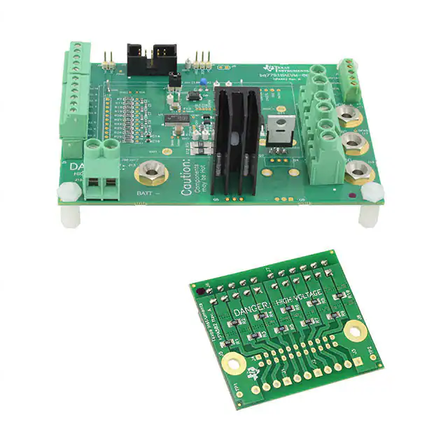
The bq77910AEVM-001 evaluation module (EVM) is a complete evaluation system for the bq77910A, a 4cell to 10-cell Li-Ion battery protection integrated circuit. The EVM consists of a bq77910A circuit module
and a resistor cell simulator module which can be used for simple evaluation of the bq77910A functions.
The circuit module includes one bq77910A integrated circuit (IC), sense resistor, power FETs, and all
other onboard components necessary to protect the cells from overcharge, over discharge, short circuit,
and overcurrent discharge in a 10-series cell Li-Ion or Li-Polymer battery pack. The circuit module
connects directly across the cells in a battery. With a compatible interface board and Windows®-based PC
software, the user can view the bq77910A registers and program the IC configuration and protection
limits.
1
2
3
4
5
6
7
Contents
Features ...................................................................................................................... 3
1.1
Kit Contents ......................................................................................................... 3
1.2
Required Equipment ............................................................................................... 3
bq77910A Circuit Module and Interfaces ................................................................................ 3
2.1
Circuit Module Connections ...................................................................................... 3
2.2
Signal Descriptions ................................................................................................ 4
bq77910A EVM Hardware Connection and Operation ................................................................. 5
3.1
Initial Considerations .............................................................................................. 5
3.2
Connecting the Cell Simulator .................................................................................... 6
3.3
Simulated Battery Connection .................................................................................... 6
3.4
Pack Connections .................................................................................................. 6
3.5
Basic Operation .................................................................................................... 7
3.6
Cell Connections ................................................................................................... 8
Software Installation ........................................................................................................ 8
4.1
System Requirements ............................................................................................. 8
4.2
Interface Adapter ................................................................................................... 8
4.3
Installing the bq77908-10-GUI-SW Evaluation Software .................................................... 10
Software Operation ........................................................................................................ 10
5.1
Menu Commands ................................................................................................. 12
5.2
Working with Register Values ................................................................................... 14
5.3
Status Section ..................................................................................................... 16
5.4
Basic Operation With Software ................................................................................. 17
5.5
Operation with Other interfaces or Hosts ...................................................................... 17
Related Documents From Texas Instruments ......................................................................... 18
bq77910A EVM Circuit Description and Configuration ............................................................... 18
7.1
Battery Voltage Clamp ........................................................................................... 18
7.2
Device Power ..................................................................................................... 18
7.3
Cell Monitor Inputs and Configuration ......................................................................... 18
7.4
Ground Connection ............................................................................................... 20
7.5
Current Sense Connections ..................................................................................... 20
7.6
Filter Capacitors .................................................................................................. 21
7.7
FET Circuits ....................................................................................................... 21
7.8
Detection Sensing ................................................................................................ 21
7.9
Output Protection Components ................................................................................. 22
Windows, Vista are registered trademarks of Microsoft Corporation.
Aardvark is a trademark of Total Phase.
SLUU855 – February 2012
Submit Documentation Feedback
bq77910AEVM
Copyright © 2012, Texas Instruments Incorporated
1
�www.ti.com
8
7.10 Reserved Pins ....................................................................................................
7.11 Flag Outputs ......................................................................................................
7.12 Thermal Sensor ...................................................................................................
7.13 ZEDE ...............................................................................................................
7.14 Programming Interface ..........................................................................................
bq77910A Circuit Module Physical Construction ......................................................................
8.1
Main Board ........................................................................................................
8.2
Resistor Cell Simulator ..........................................................................................
22
22
22
22
22
23
23
32
List of Figures
25
...........................................................................................................
Successfully Updated TI USB Interface Adapter .......................................................................
EVM Connection for Communication and Programming .............................................................
GUI with Communication Established ..................................................................................
Communication Selection Window ......................................................................................
Commands Without Communication Established .....................................................................
Register Section ...........................................................................................................
Status Section..............................................................................................................
Polling Status with Under-Voltage Condition ..........................................................................
Top Silkscreen .............................................................................................................
Top Assembly ..............................................................................................................
Top Layer ...................................................................................................................
Layer 2 ......................................................................................................................
Layer 3 ......................................................................................................................
Bottom Layer ...............................................................................................................
Bottom Silkscreen .........................................................................................................
Bottom Assembly ..........................................................................................................
Schematic Diagram Page 1 ..............................................................................................
Schematic Diagram Page 2 ..............................................................................................
Resistor Simulator Top Silkscreen ......................................................................................
Resistor Simulator Top Layer ............................................................................................
Resistor Simulator Bottom Layer ........................................................................................
Resistor Simulator Top Assembly .......................................................................................
Resistor Simulator Bottom assembly ...................................................................................
Resistor Simulator Schematic Diagram ................................................................................
1
Ordering Information ........................................................................................................ 3
2
Cell Connections ............................................................................................................ 4
3
PACK Connections ......................................................................................................... 4
4
Programming Interface Connections ..................................................................................... 4
5
Test Header Signals ........................................................................................................ 5
6
Control and Status Connections .......................................................................................... 5
7
Adapter Cable Pinout ..................................................................................................... 10
8
Status Section Indicator Colors .......................................................................................... 16
9
Cell Count Component Configuration ................................................................................... 19
10
bq77910A Circuit Module Bill of Materials ............................................................................. 28
11
Performance Specification Summary ................................................................................... 32
12
Resistor Simulator Bill of Materials ...................................................................................... 36
1
2
3
4
5
6
7
8
9
10
11
12
13
14
15
16
17
18
19
20
21
22
23
24
Basic EVM Setup
7
9
11
12
13
13
14
16
16
23
24
24
25
25
26
26
27
30
31
32
33
34
35
36
38
List of Tables
2
bq77910AEVM
SLUU855 – February 2012
Submit Documentation Feedback
Copyright © 2012, Texas Instruments Incorporated
�Features
www.ti.com
1
Features
•
•
•
•
•
•
1.1
Complete evaluation system for the bq77910A 4-cell to 10-cell Li-Ion and Li-Polymer battery protector
Populated circuit module for 10-cell parallel FET configuration for quick setup
– Pads for components for configuration of additional cell counts and series FETs
Power connections available on terminal blocks or banana jacks
Control and status signals available on terminal blocks
Resistor cell simulator for quick setup with only a power supply
PC software available for configuration
Kit Contents
•
•
•
bq77910A circuit module
Resistor cell simulator
Set of support documentation
Table 1. Ordering Information
EVM Part Number
Chemistry
Configuration
Capacity
bq77910AEVM-001
Li-Ion
10 cells
Any
NOTE: Although capacity is shown as "Any," practical limits of the physical construction of the
module will typically limit the operation of the EVM to a 1P or 2P battery construction. Refer
to the physical construction section for board details.
1.2
Required Equipment
The following equipment is required to operate the bq77910A EVM in a simple demonstration:
• DC power supply, 0-43V at 0.5A
• DC voltmeter or oscilloscope
• DC power supply, ~3V at .1A or an approximately 15k-Ω 1/4W resistor
• Test leads to connect equipment
The following equipment is required to operate the bq77910A with a more extensive demonstration:
• TI USB-TO-GPIO interface adapter
• Computer with USB port and compatible Windows 32 bit operating system
• Electronic load
• Additional power supplies
• TI bq77908-10-GUI-SW Evaluation Software (see Section 4)
2
bq77910A Circuit Module and Interfaces
The bq77910A circuit module contains the bq77910A IC and related circuitry to demonstrate the features
of the IC. A FET with heatsink is provided for the high current discharge path. A lower current FET is
provided for the charge path. A thermistor provides temperature sensing for the device. Other components
provide support for the IC and connections to the board.
2.1
Circuit Module Connections
Connections are provided for the following interfaces:
• Direct cell connections
• PACK connections
• Programming interface
SLUU855 – February 2012
Submit Documentation Feedback
bq77910AEVM
Copyright © 2012, Texas Instruments Incorporated
3
�bq77910A Circuit Module and Interfaces
2.2
www.ti.com
Signal Descriptions
Signals available on the EVM are described in this section. For details on the location and connector
types, refer to the physical construction section. High current signals can be connected at either the
terminal block or banana jack. Refer to the physical construction section for identification.
Cell connections are described in Table 2. The default board assembly supports only 5 cells, so the upper
cell connections are not used. CELL0 and CELL5 are connected to the high current paths on the board
through 0-Ω resistors. This allows operation of the resistive cell simulator without external connections. If
the on-board resistors are removed, connections must be made off the board. Refer to the physical
construction section for resistor identification. Cell connection sequence is described in Section 3.6.
Table 2. Cell Connections
Reference
Designator
Pin Number
J13, J15
All
BATT–
Negative electrode of first (bottom) cell, high current connection
J5
6
CELL0
Negative electrode of first (bottom) cell, optional separate monitor connection to
cell
5
CELL1
Positive electrode of first (bottom) cell
4
CELL2
Positive electrode of second cell
3
CELL3
Positive electrode of third cell
2
CELL4
Positive electrode of fourth cell
1
CELL5
Positive electrode of fifth cell,
5
CELL6
Positive electrode of sixth cell
4
CELL7
Positive electrode of seventh cell
3
CELL8
Positive electrode of eighth cell
2
CELL9
Positive electrode of ninth cell
1
CELL10
Positive electrode of tenth cell, optional separate monitor connection to cell
All
PACK+
Most positive cell output, high current connection, shared with PACK+
J4
J10, J11
Signal
Description
Load connections are described in Table 3.
Table 3. PACK Connections
Reference
Designator
Pin Number
J10, J11
All
PACK+
Positive output of evaluation board, shared with the battery high current
connection
J12, J14
All
DSG–
Negative output of evaluation board for discharge
J16, J17
All
CHG–
Negative input to evaluation board for charge
Signal
Description
Programming signals are described in Table 4. J3 signals are 3.3V logic level.
Table 4. Programming Interface Connections
Reference
Designator
Pin Number
J3
1, 2, 5, 7, 8
J2
4
Signal
Description
Not used
3
PGM
Control signal for EEPROM programming voltage.
4
ZD
Control signal for device ZEDE
6
GND
Signal reference for the IC
9
ECLK
Serial interface clock connection
10
EDATA
Serial interface data connection
1
14V
Regulated 14V input for IC programming
2
GND
Signal reference for the IC
bq77910AEVM
SLUU855 – February 2012
Submit Documentation Feedback
Copyright © 2012, Texas Instruments Incorporated
�bq77910A EVM Hardware Connection and Operation
www.ti.com
Test header or pattern signals are described in Table 5.
Table 5. Test Header Signals
Reference
Designator
J1
J6
J8
Usage
Pin Number
Signal
Description
Default: shunt
installed for
normal
operation.
Remove shunt
for U1 supply
current
measurement
1
Battery feed
Power feed to 100-Ω shunt resistor
2
BAT
Output of 100-Ω shunt resistor to IC BAT pin
Default: no
shunt. Install
shunt to hold
ZEDE high
1
VREG
IC regulator output
2
ZEDE
IC zero delay test point and input pin, also connected to J3
3
PD
Pull down resistor for strong pull down of ZEDE if required
Not populated.
Alternate test
point or remote
thermistor
connection
1
TS
IC temperature sense pin
2
GND
Signal reference for the IC
Control and status signals are provided on terminal blocks. These signals are described in Table 6.
Table 6. Control and Status Connections
Reference
Designator
Pin Number
J7
1
TS
IC TS signal through a resistor
2
GND
Signal reference for the IC
1
CHGCTL
Control signal for charger detection, connects through a resistor to the IC CHGST
pin
2
DSGFLAG
Diode and resistor isolated DSG signal
3
CHGFLAG
Diode and resistor isolated CHG signal
J9
3
Signal
Description
bq77910A EVM Hardware Connection and Operation
This section describes the connection of the circuit module and EVM and simple operation in its default
configuration.
3.1
Initial Considerations
Boards are tested after assembly with a basic functional test. This test may not check every connection on
the board. Boards should be checked for function in the user’s environment before relying on the safety
features of the board. Operation of the board with test equipment before connecting cells is recommended
and described in this document.
The default configuration of the board is 10 cells with parallel FETs. Modifying the EVM for different cell
counts or FET configuration requires solder connections. It is recommended that the user familiarize
themselves with operation of the board in the default configuration before modifying the board, and check
the operation of the board with test equipment after any modification. Configuration of the board is
described in Section 7.
Be sure to observe the cautions and warnings in this document.
A variety of connections are provided on the EVM. The manufacturer's rating for the terminal blocks for
Pack and Battery connections is 32A nominal. Parallel connections are provided for high current
operation. The banana jacks are rated at 15A. Safety agency ratings may be lower than the manufacturer
ratings, limit currents to appropriate values for your evaluation. Cell monitor terminal blocks and the
control signal terminal blocks are rated at lower currents and should not be used for high current paths.
SLUU855 – February 2012
Submit Documentation Feedback
bq77910AEVM
Copyright © 2012, Texas Instruments Incorporated
5
�bq77910A EVM Hardware Connection and Operation
www.ti.com
A communication interface is not required for basic operation, and it should be connected to the computer
and EVM circuit module only after proper installation of software. The software along with an appropriate
communication interface allows setting the programmable safety limits of the device and checking the
status after fault detection. Installation of the software and its use are described in a later section.
3.2
Connecting the Cell Simulator
The cell simulator consists of headers to mate the board and ten (10) 200-Ω resistors to divide the battery
voltage between the inputs. Power is provided through the Cell0 and Cell10 connections on the terminal
block headers. Various test points are provided on the board. Refer to physical construction section for
additional details.
• Be certain no power is applied to the board.
• Unplug the screw terminal blocks from J4 and J5 of the EVM and save these for later use.
• Plug the cell simulator board onto J4 and J5. Support may be required on the bottom of the EVM while
the connectors are pressed together firmly.
CAUTION
Do not connect or remove the cell simulator board while power is applied to the
EVM. The resistor pull down or up from intermittent connections will overstress
the device inputs.
3.3
Simulated Battery Connection
Connect a power supply between BATT– (negative) and PACK+ (positive). This power supply will connect
to the resistor cell simulator through default connections on the bq77910A circuit module.
3.4
Pack Connections
A load or charger is connected to the pack terminals using the terminal blocks provided. It is
recommended that the load or charger be connected with the current switched off to prevent arcing or
transients during connection of the wires to the terminal blocks. Charger detection is required for the
bq77910A with a signal at the CHGST pin. Charger detection can be provided by connecting a resistor
from the CHGCTL terminal of the board to the PACK supply, or with a logic level voltage supply for
evaluation. An external resistor is required due to the low resistance pull down on the board. The selected
resistor should keep the CHGST voltage above the VCHG_DET1 data sheet threshold over the entire
evaluation voltage range while limiting the power in the 1k-Ω pulldown resistor to 1/16W or less. A 15k-Ω
1/4W resistor is typically suitable for the default configuration, a smaller value may be required for low
voltage or if the configuration is changed.
WARNING
The CHGCTL should not be tied to the power supply without the
external resistor since the 1k resistor on the board will become
very hot and may damage the board.
Although designed for 30A operation, the board may not dissipate enough power to operate without
exceeding all component ratings. The user should monitor the temperature of the board and components
during evaluation and provide cooling air and/or heatsinks as required for operation. The thermal sensor
on the board may not respond to protect the FETs from damaging temperatures due to its location and
possible thermal gradients on the board.
6
bq77910AEVM
SLUU855 – February 2012
Submit Documentation Feedback
Copyright © 2012, Texas Instruments Incorporated
�bq77910A EVM Hardware Connection and Operation
www.ti.com
CAUTION
The bq77910A circuit module may be damaged by over temperature. To avoid
damage, monitor the temperature during evaluation and provide cooling as
needed for your system environment.
WARNING
The bq77910A circuit module may become hot during operation
due to dissipation of heat. Avoid contact with the board. Follow all
applicable safety procedures applicable to your laboratory.
CAUTION
Some power supplies can be damaged by application of external voltages. If
using more than 1 power supply check your equipment requirements and use
blocking diodes or other isolation techniques as needed to prevent damage to
your equipment.
The connection of the EVM will look similar to Figure 1.
~ 15k ohm
Resistor
Cell
Simulator
“Charger”
supply
+
+ Load
-
“Battery”
supply
+
Figure 1. Basic EVM Setup
3.5
Basic Operation
The following steps are suggested for basic operation of a default EVM with the cell simulator and the
default configuration in EEPROM.
1. Confirm the cell simulator board is installed on the EVM.
2. Connect a power supply between the BATT– (negative) and PACK+ (positive) terminals.
3. Connect a 15k-Ω 1/4W resistor to the CHGCTL terminal of the board.
4. Set the bench supply to approximately 36V.
5. Connect a disabled load between the DSG– (negative) and PACK+ (positive) terminals.
SLUU855 – February 2012
Submit Documentation Feedback
bq77910AEVM
Copyright © 2012, Texas Instruments Incorporated
7
�Software Installation
www.ti.com
6. Wake up the part by momentarily connecting the 15k resistor to the bench supply positive.
7. Monitor the CHG and DSG test points using a meter or oscilloscope as desired.
8. Enable the load with a nominal 0.2A or other current within the capability of the supply.
9. Increase the bench supply voltage to ~43V and observe the CHG test point goes low.
10. Reduce the voltage to ~36V and observe the CHG test point returns high.
11. Decrease the voltage to ~25V and observe the DSG test point goes low and the load current drops.
The device will shut down after 9 seconds at low voltage.
12. Remove the load and connect the CHGCTL resistor to the supply to simulate a charger.
13. Increase the supply voltage to ~36V and observe the DSG test point goes high, and if the load is reconnected that current flows again.
3.6
Cell Connections
For initial evaluation, it is suggested power supplies be used for cell simulation to observe the behavior of
the device. An isolated power supply with a resistor connected across its terminals may be connected to
test points on the resistor simulator to vary the voltage above or below the voltage of the other cells, or a
similar configuration may be used. The smaller the resistor value, the more current is required from the
battery simulator power supply and the smaller the influence on the voltages if cell balancing is operated.
Whether power supplies or cells are used, inductance in the high current path should be minimized.
Inductance in this path can cause inductive transients at the board when the load current is stopped or the
bq77910A opens the discharge FET with current flow. Use heavy gauge wires for the high current
connections; minimize inductances by keeping leads close together.
When connecting cells to the EVM, the user should use care not to exceed the absolute maximum ratings
of the device. The bq77910A is designed with open cell (wire) detection, however fixturing should not pull
un-connected signals up or down. Signal reference (VSS) for the part is from the BATT– terminal of the
EVM, and this lowest potential should be connected first. Cells should be connected in sequence from
lowest to highest voltage as described in the data sheet. When terminating the cells to the removable
terminal blocks prior to connection to the EVM, the following steps are recommended:
1. Be sure the charger and any load is disconnected (CHGCTL is open).
2. Connect the cell stack negative high current terminal to the EVM BATT– terminal.
3. Connect the lower cell group to the J5 connector.
4. Connect the upper cell group to the J4 connector.
5. Connect the cell stack positive high current terminal to the EVM PACK+ terminal.
6. When removing cells, remove any charger and CHGCTL connection, then disconnect in the reverse
order.
4
Software Installation
This section describes how to install the software for the bq77910AEVM-001.
The bq77908-10-GUI-SW supports the bq77910A and is described in this document as bq77910A
evaluation software.
4.1
System Requirements
The bq77910A evaluation software requires a 32-bit version of Windows XP, Windows Vista® or
Windows 7. The computer must also have Microsoft .NET framework version 2.0 or higher installed.
Examples in this document are from Windows XP.
4.2
Interface Adapter
The bq77910A evaluation software supports either the TI USB-TO-GPIO adapter (TI USB Interface
Adapter) or the Total Phase Aardvark™ to provide communication with the EVM board from the computer.
The , the Aardvark must be selected if desired. The EVM connector supports the TI USB Interface
Adapter, a special cable must be constructed if you wish to use the Aardvark.
8
bq77910AEVM
SLUU855 – February 2012
Submit Documentation Feedback
Copyright © 2012, Texas Instruments Incorporated
�Software Installation
www.ti.com
4.2.1
TI USB Interface Adapter
The TI USB Interface Adapter is default option for the bq77910A evaluation software. Its pinout is
compatible with the bq77910A EVM board J3 connector.
The TI USB Interface Adapter http://focus.ti.com/docs/toolsw/folders/print/usb-to-gpio.html is actually a
separate EVM from Texas Instruments and its default firmware is not compatible with the bq77910A. If the
firmware has already been updated to version 2.0.19 to work with other BMS-HCE products, additional
update is not required. If required, update the firmware using the following steps.
1. Obtain the USB to GPIO EVM Firmware Loader from
http://focus.ti.com/docs/toolsw/folders/print/usb2gpio-loader-sw.html or search from power.ti.com.
2. Download, extract and run the installer.
3. Installation requires the Microsoft .NET connection software. If a suitable version is not found on the
system by the installer, the user will be prompted to obtain and install .NET.
4. Connect the TI USB Interface Adapter to the computer with the USB cable. The green LED should
illuminate.
5. Run the program, typically from Start>Run>Texas Instruments> USB-TO-GPIO Firmware Loader.
6. Detailed instructions are provided in the Readme.txt file.
CAUTION
Do not disconnect the USB cable to the Interface Adapter during firmware
update. Loss of power may leave the adapter with corrupt firmware and be
unable to further update the firmware.
7. If you want to be able to return to the original configuration, backup the installed firmware before
update.
8. Load and Update to the 2.0.19 version using the instructions provided.
9. If an error occurs, do not unplug the adapter. Re-try loading, load a different firmware or re-start the
software and repeat until a load is successful.
10. After successful update, the window should appear as Figure 2.
11. After update, exit the program.
Figure 2. Successfully Updated TI USB Interface Adapter
SLUU855 – February 2012
Submit Documentation Feedback
bq77910AEVM
Copyright © 2012, Texas Instruments Incorporated
9
�Software Operation
4.2.2
www.ti.com
Aardvark Adapter
Although the Total Phase Aardvark adapter will physically mate to the EVM J3 connector, the pinout is
incompatible. A special interface cable must be constructed to use the Aardvark. Refer to the schematics
and Table 7 below for information.
CAUTION
Do not connect the Aardvark to the EVM without a properly constructed cable.
Damage may result to the EVM and/or Aardvark.
Table 7. Adapter Cable Pinout
IC Pin Name or Description
4.3
USB-TO-GPIO (Mates to J3)
Aardvark
Pin
Signal
Pin
Signal
VSS – signal reference
6
GND
2
GND
SCLK
9
SCL
1
SCL
SDATA
10
SDA
3
SDA
ZEDE – communication enable
4
GPIO4
5
MISO/GPIO
Programming voltage control signal for
EEPROM
3
GPIO5
7
SCLK/GPIO
Installing the bq77908-10-GUI-SW Evaluation Software
Find the latest software version in the bq77908-10-GUI-SW Evaluation Software tool folder
http://www.ti.com/tool/bq77908-10-gui-sw or search from power.ti.com. Check periodically for software
updates. Use the following steps to install the bq77910A Evaluation Software:
1. Copy the archive file to a directory of your choice, extract and run the bq77910A setup.msi installer.
2. Follow the instructions and make selections as required on the setup windows selecting next as
required.
3. On the last window, select "close" to complete the bq77910A software installation.
5
Software Operation
This section describes connection of the communication interface to the EVM and operation of the
software.
Although the software will run without connection to a powered device it is recommended to have the
device on when starting the software. Figure 3 shows connections for operation with the GUI software.
10
bq77910AEVM
SLUU855 – February 2012
Submit Documentation Feedback
Copyright © 2012, Texas Instruments Incorporated
�Software Operation
www.ti.com
USB
Interface
Adapter
PC
USB
“Programming”
supply
+ (14V)
~ 15k ohm
Resistor
Cell
Simulator
“Charger”
supply
+
+ Load
-
“Battery”
supply
+
Figure 3. EVM Connection for Communication and Programming
To connect the computer to the GUI and start the software use the following steps:
1. Connect the TI USB interface adapter to the computer.
2. Connect the 10 pin connector from the interface adapter to the EVM J3.
CAUTION
The communication interface is not isolated on the EVM. Be sure no ground
potential exists between the computer and the EVM. Also be aware that the
computer will be referenced to the Battery- potential of the EVM.
3.
4.
5.
6.
Remove any shunt installed on J6 so the interface can control ZEDE.
Connect the "battery" power supply to the EVM, adjust to approximately 30 to 40VDC.
Wake the bq77910A by connecting CHGCTL high.
Start the software, typically using Start > All Programs > Texas Instruments > bq77908-bq77910
Evaluation.
When started, the software will look for the communication interface and the device. When communication
is established with the device, the main window appears as shown in Figure 4.
SLUU855 – February 2012
Submit Documentation Feedback
bq77910AEVM
Copyright © 2012, Texas Instruments Incorporated
11
�Software Operation
www.ti.com
Figure 4. GUI with Communication Established
Other than the menu selections, the software window has 3 sections. In the bottom border is a status
section. The middle section is a register section. The top section is a status area useful for checking the
device status when a fault is detected. Details are described in following sections.
5.1
5.1.1
Menu Commands
Help Menu
The Help > About menu selection displays version information about the program.
5.1.2
Setup Menu
The Setup > Communication selection allows selection of either the USB Interface Adapter or the
Aardvark. Default is the TI USB Interface Adapter and this window will not be needed. Selecting the Save
and Exit button will check for the adapter, If the selected adapter is not present, a communications error
window will appear. Selecting OK in the window will return to the Communication Selection Window. To
exit without having the selected adapter connected, use the close window tool (red X button). Selection of
an adapter other than the 2 shown is not supported.
12
bq77910AEVM
SLUU855 – February 2012
Submit Documentation Feedback
Copyright © 2012, Texas Instruments Incorporated
�Software Operation
www.ti.com
Figure 5. Communication Selection Window
5.1.3
Commands Menu
Most commands are only available after communication is established with the device. Figure 6 shows the
command window when Communication is not yet established.
Figure 6. Commands Without Communication Established
The communication status in the bottom border of the window shows the adapter in use and the device
communication status. If the software is started and the adapter is not found, a Communication Error
message box is displayed. Selecting OK on the box will display the main window. If the device is not
recognized, a Device Not Found box is displayed. Selecting OK to this box will also display the main
window. The communication fault will be displayed in the status area of the window. Communication can
be re-tried by selecting the menu command Commands > Find Target. Once Communication is
established with the part, the Find Target command is no longer available.
The other commands relate to the register section. The register section is shown in Figure 7. Two sets of
registers are displayed, the right section can display the EEPROM settings, the left side can display the
volatile registers waiting to be programmed in the EEPROM. When the software is first started, all values
are shown as zero.
SLUU855 – February 2012
Submit Documentation Feedback
bq77910AEVM
Copyright © 2012, Texas Instruments Incorporated
13
�Software Operation
www.ti.com
Figure 7. Register Section
The Read Volatile Registers command will read the values from the registers in the part and display them
in the GUI window. When a part is first powered, these will typically be zero. When connecting to a
powered part, they will likely contain residual values.
The Read EEPROM Registers command will read the EEPROM values from the device and display them
in the EEPROM registers section of the window for viewing. This is a viewing operation and data
manipulation is not allowed in the displayed EEPROM data.
The Read All Registers command reads both the volatile and EEPROM registers from the device and
displays the values.
The Copy EEPROM to Volatile command will copy the EEPROM register values to the corresponding
volatile registers and display both in the GUI. This is a good starting point for making incremental changes
to the device settings.
The Verify Volatile Registers command checks whether the volatile registers match the contents of the
device. This can be useful as a check before programming the EEPROM.
The Program EEPROM command will write the volatile register values.
5.1.4
File Menu
The Load Registers from File command will read a properly formatted file and fill the volatile register
section with the values. This is useful to load a device with a saved configuration. A windows navigation
tool allows selection of the file. While files could be edited, it is recommended to load files saved by the
software, and if any editing is performed on the file, check all values before programming the device.
The Save Registers to File command will create a file. A windows navigation tool allows selection of the
location and file name. Files have the .cfg extension.
The Exit command will exit the program.
5.2
Working with Register Values
When the software initially connects to a device it will copy that device's EEPROM to its volatile registers
and display those results. Since the device does not know if power has been lost to the device, the
register display may be stale. If the device has been changed or power cycled to the part, the registers
should always be read before making changes. If a file is loaded with values matching the displayed
values, the software will not know the data is different from the part. Reading the registers or copying
EEPROM values to the volatile registers is recommended before any change.
14
bq77910AEVM
SLUU855 – February 2012
Submit Documentation Feedback
Copyright © 2012, Texas Instruments Incorporated
�Software Operation
www.ti.com
EEPROM values are displayed but are not directly editable in either the device or the GUI. Changes are
made to a volatile register set by changing the volatile register value which is written to the volatile register
in the device and later written to the device EEPROM by the programming process. Changes in the
volatile registers do not affect operation of the device until written into the EEPROM.
The proper device must be selected in the device box before changing register values. This selection is
entered by the user rather than read by the software. Select the "bq77910" button for the bq77910A.
Leaving the default bq77908 device selection limits the range of the cell count that can be programmed to
the device.
Values in the Volatile Registers section can be typically be changed in three ways:
• Loading a register file
• Changing a check box or drop-down selection
• Entering a data value in the box corresponding to the register name
The SYS_CFG register bits are displayed as selection boxes, these are green for a value “0” and orange
for a value “1”.
The following steps describe changing a device EEPROM setting on the EVM using the GUI with a
connected adapter:
1. Power the EVM (device) with the "battery" supply, and wake it up with charger detection.
2. Maintain a logic high on the CHGCTL pin of the EVM (CHGST device pin).
3. Copy the EEPROM values to the volatile registers with the Copy EEPROM to Volatile command.
4. Edit the values in the “Volatile Registers” section as desired.
5. Provide a 14 +/– 0.5V at approx 0.1A programming voltage at the EVM J2 connector.
6. Select the “Program EEPROM” command.
7. After a short delay a programming complete status window should appear. Select OK in this window.
8. Disconnect the programming voltage from the EVM J2 connector.
Programming the EEPROM from a file uses a very similar sequence. This can be useful in evaluation
when replacing a device or duplicating a design on a small number of boards. The following steps
describe programming a device EEPROM on the EVM from a saved configuration file using the GUI with a
connected adapter:
1. Power the EVM (device), and wake it up with charger detection.
2. Maintain a logic high on the CHGCTL pin of the EVM (CHGST device pin).
3. Select the File > Load Register File command, navigate to and open the desired file.
4. Provide a 14 +/– 0.5V at approx 0.1A programming voltage at the EVM J2 connector.
5. Select the “Program EEPROM” command.
6. After a short delay a programming complete status window should appear. Select OK in this window.
7. Disconnect the programming voltage from the EVM J2 connector.
After programming it may be necessary to clear fault status since programming requires communication
with the device and that requires setting ZEDE high. ZEDE high may make the part respond to noise.
SCC is typically the lowest value threshold in the device and is common after programming or other
Communication with the part, depending on the device settings and operating environment.
CAUTION
While the software may be useful for producing a small number of boards, it is
not intended as a production programming tool. Accidental manipulation of the
data between when the file is loaded and when the programming command is
sent is not prohibited.
SLUU855 – February 2012
Submit Documentation Feedback
bq77910AEVM
Copyright © 2012, Texas Instruments Incorporated
15
�Software Operation
www.ti.com
During programming the software checks that the device volatile registers match the values shown. If they
do not match, an error message is displayed. Continuing with programming when the values do not match
will unexpectedly alter the configuration of the device. If the error is displayed it is recommended to read
the volatile registers to examine the contents, correct any communication error and re-start the software or
device as needed for proper programming.
5.3
Status Section
The status section of the GUI is shown in Figure 8. This section allows the user to display internal status
registers of the devices fault condition. This data is not part of normal operation of the device and is not
shown in the data sheet. Accessing the data is disruptive to the device, however it can be beneficial in
evaluation.
Figure 8. Status Section
The status is read by selecting the Polling "Enable" button on the left side of the status section. This will
periodically set ZEDE high to the device, read the status registers, and return ZEDE low. The polling
period can be selected with the drop down box next to the button. The button function and label change to
"Disable". The button label indicates the action of the next button actuation.
A consequence of polling is that a pending fault delay will be terminated by the status read. Polling is
typically independent of any system change and a fault may be recorded as soon as the poll occurs. This
may lead to unexpected results in evaluation. The following describe a couple examples which may occur:
• The user has selected a 2 second under voltage delay and wants to observe the timing on a scope.
The user leaves polling active and decreases the device voltage. The poll occurs just after the voltage
drops and the zero delay causes the fault to be registered. The FETs turn off and the user thinks the
delay setting is not working. The situation here is the poll set ZEDE high and terminated the under
voltage delay.
• The user is polling status to watch faults. CHGST is tied high to prevent the part from shutting down
due to under voltage. The user begins switching currents and is surprised when a SCC fault occurs.
Observing the sense resistor voltage, the user does not see a charge current. The situation here is the
poll set zero delay and eliminates noise filtering on the current. The SCCT is typically a low and thus
most sensitive to any noise; having CHGST high prevents recovery from the fault.
The values display in several colors. See Table 8.
Table 8. Status Section Indicator Colors
Color
Meaning
gray
status is not read
bright green
device is polling and status is normal with connected device, or adapter is not
connected
bright red
device is polling and status is fault
dark green or dark red
device is not polling and value is residual from last poll
Figure 9 shows a typical status display polling with undervoltage.
Figure 9. Polling Status with Under-Voltage Condition
16
bq77910AEVM
SLUU855 – February 2012
Submit Documentation Feedback
Copyright © 2012, Texas Instruments Incorporated
�Software Operation
www.ti.com
Another use of the status section is to determine the reason the part has turned off the FETs. For example
if during test the EVM has turned off the FETs but the VREG is still on, the interface might be connected
and the status polled to see what fault the device identifies.
5.4
Basic Operation With Software
The following steps are suggested for exercise of more of the device features using the EVM in its default
10-cell configuration and EEPROM settings. The board is connected as shown in Figure 3. Remember
that timing will be incorrect as described in Section 5.3.
1. Install the software.
2. Connect the USB Interface Adapter to the computer with the USB cable.
3. Remove the screw terminal blocks from J4 and J5 and save for later use. Connect the cell simulator
board to the bq77910A main board J4 and J5. Support the under side of the EVM board as the
connectors are pressed together.
CAUTION
Do not connect or remove the resistive cell simulator from the board with power
applied. The resistor pull down or up from intermittent connections will
overstress the device inputs.
4. Connect the 10 pin ribbon cable from the USB Interface Adapter to the EVM J3.
5. Connect an isolated power supply negative to BATT– and positive to PACK+. Adjust the voltage to
approximately 32V.
6. Connect a ~15k resistor from the power supply positive to the CHGCTL terminal. This will wake the
part; leave the resistor connected.
7. Start the software.
8. Connect a disabled load to the pack terminals.
9. Select the polling Enable button in the software window.
10. Observe the status values are bright green.
11. Set a current on the load within the capability of the supply and board.
12. Decrease the power supply voltage to approximately 25V. Observe using load current stops and the
UV status indicator turns red.
13. Increase the supply voltage to approximately 31V. Observe the UV indicator turns green.
14. Load current may not resume until the load is disabled or disconnected.
15. Increase the supply voltage to approximately 43V. Observe the OV status indicator turns red.
16. Decrease the power supply voltage to approximately 32V. Observe that the OV indicator turns green.
17. Disable polling.
18. Disable the load.
19. Set the supply to 0V and turn off equipment.
5.5
Operation with Other interfaces or Hosts
The bq77908-10-GUI-SW software does not support other interfaces.
Communication with the bq77910A from other hosts should be straightforward. Refer to the datasheet for
timing and interface details. On the EVM, zero delay mode can be set to allow communication using a 0.1"
shunt (not provided) at J6 pins 1 to 2, or a signal at ZD on J3. To program, the on-board programming
voltage switch can be used by controlling the PGM signal on J3. Signals should be 3.3V CMOS levels.
SLUU855 – February 2012
Submit Documentation Feedback
bq77910AEVM
Copyright © 2012, Texas Instruments Incorporated
17
�Related Documents From Texas Instruments
6
www.ti.com
Related Documents From Texas Instruments
To obtain a copy of any of the following TI document, call the Texas Instruments Literature Response
Center at (800) 477-8924 or the Product Information Center (PIC) at (972) 644-5580. When ordering,
identify this document by its title and literature number. Updated documents can also be obtained through
the TI Web site at www.ti.com.
Document
bq77910A Multi-Cell Li-Ion/Polymer Precision Protector Data
Sheet
7
Literature Number
SLUSAV6
bq77910A EVM Circuit Description and Configuration
This section describes the circuit on the bq77910A circuit module and how to configure it for changes the
user may want to make to the board for specific evaluations. In many cases, an EVM schematic is used
as a starting point for a circuit design. This can result in extra components on the product design which
are not needed but take up space and in some cases add unnecessary expense. Refer to the schematic
in the physical construction section while reading the following descriptions. Note that the schematic has 2
pages, the first shows the main functions, the second page shows primarily cell count configuration and
protection components.
7.1
Battery Voltage Clamp
The TVS diode D9 provides a clamp for transients on the pack. A common transient is due to system
inductances and sudden load shutoff. The breakdown voltage of D9 should be set near or below the 5V
per cell abs max of the device. As a transient pushes the voltage up the I-V curve, a substantial device
here reduces the demands on other clamping components in the system which may be needed to protect
the device. Alternatives to D9 might be to control the system inductance and current switching rate, use
capacitance to absorb transients, or other transient protectors such as MOVs where appropriate.
7.2
Device Power
The device is powered through the BAT pin. C12 is a bypass capacitor near the IC, the footprint is large to
make it easy to mount larger capacitors in case this is desired in evaluation. R5 and J1 provide a way to
measure current to the device during evaluation and are not needed in an application. D2 provides power
from the battery to the IC and prevents the IC power from being pulled down when the battery voltage dips
suddenly due to a heavy load on the battery. C2 provides an operating reservoir for device current during
battery voltage droop. D1 limits the voltage to the BAT pin preventing over voltage from rectification of
transients by D2.
Power is provided through R4. The 200-Ω resistor provides for a voltage drop when an over voltage
charger pulls down BAT through D8. For lower cell counts, this resistor may be a smaller value. R3 is a 0Ω connection to the high current battery positive connection BATT+ which is shared with the PACK+. This
jumper is provided in case the user wants to power the part from the current monitor line instead.
7.3
Cell Monitor Inputs and Configuration
The cell monitor inputs are provided through a RC filter network. The series resistors RVCX connect the
cells to the device to allow voltage measurement and limit the balancing current. Balancing current is
approximately the cell voltage divided by twice the resistor. The EVM is circuit is designed to use the
internal balancing path at near the maximum current. The 47 Ω RVCX value on the EVM is nominally within
10% of the 50-Ω minimum recommended in the datasheet and will prevent exceeding the absolute
maximum balancing current up to 4.3V per cell. The input capacitance is typically connected between cell
inputs, except the capacitances at VC10 and VC11 are connected to ground to avoid pushing the inputs
below ground during transients. The capacitance should not be increased beyond the 1 μF shown since
the capacitors are discharged into the device during balancing. The filter effect will both reduce cell
transients to the device inputs, and slow voltage recovery after balancing. The resulting time constant is
complicated due to the multiple components but relatively short due to the small resistors used for high
balancing current. Due to the cell input voltage measurement after balancing, the time constant (RVCX)
should not be made too large.
18
bq77910AEVM
SLUU855 – February 2012
Submit Documentation Feedback
Copyright © 2012, Texas Instruments Incorporated
�bq77910A EVM Circuit Description and Configuration
www.ti.com
The user should note there are two limits implied by the absolute maximum cell-to-cell differential rating of
the part. One is the applied differential voltage, or 5V on any cell regardless of the other inputs. Note also
this is an applied voltage, not the voltage induced by the part during balancing, which may be higher. The
second voltage limit is the voltage to ground the cumulative voltage from summing the individual limits.
Since the input filter time constant is small, clamping the inputs to safe values may be required. While a
zener or TVS diode per cell may be a suitable way to protect the device in some applications, the EVM
provides patterns D12 to D18 to clamp the inputs for cells 10 to 4 to ground. The top cell input is clamped
(VC1 with D12 on the EVM), and cell 4's input, VC7 is clamped with D18 on the EVM since this input
showed more sensitivity than others in testing. For nominal transients, these clamps in conjunction with
the capacitors between cells should hold the inputs to safe values, however different or additional
clamping may be required in evaluation or the target application.
The EVM has resistor jumper positions and is populated to connect to the cells with N+1 wires where N is
the number of cells. R42 connects the high current BATT– connection to the lowest cell monitor point.
Similarly R59 connects cell 10 input to the high current path through R3. Additional resistor patterns R53
to R58 allow the same connections when the board is configured for other series cell counts. The board
may be configured to monitor the cell voltages directly at the cells (N+3 wires) by removing R42 and R59
or its equivalent.
When configuring the part for fewer than 10 cells, the unused inputs should not be left floating and must
be connected to avoid exceeding absolute maximums. The EVM provides patterns to allow flexible
connections. The unused pin group may be connected together on the EVM by shorting the capacitors
between them or shorting the appropriate resistor jumper positions R60 to R64. The unused pin group
then needs to be connected to a safe level, either to the top cell through one of the unused cell RVCX
patterns or to the highest used VCx pin using the appropriate R61 to R65. When configuring for fewer
than 10 cells and using the cell simulator, be sure to remove components to avoid parallel paths. Due to
the flexibility allowed by the EVM for configuration it is recommended the evaluator study the schematic
before modifying the board to achieve their desired configuration. Table 9 shows possible configurations
for different cell counts assuming use of the cell simulator, retaining the N+1 wiring plan and adjusting the
transient protection. The board will operate at a lower cell count without the transient protection
adjustment, but the user should be sure they provide adequate protection for the IC in the evaluation and
system design to prevent damage. The table describes a change from the 10-cell default to one of the
other configurations, the users should check configurations if multiple changes are made. D12 is shown
removed in the table for less than 10 cells to avoid any possible leakage current or unexpected clamp
during evaluation.
Table 9. Cell Count Component Configuration
Cell Count/
Reference
Designator
10 Cells
(Default)
9 Cells
8 Cells
7 Cells
6 Cells
5 Cells
4 Cells
C3
installed
Remove
installed
installed
installed
installed
installed
C5
installed
installed
Remove
installed
installed
installed
installed
C6
installed
installed
installed
Remove
installed
installed
installed
C7
installed
installed
installed
installed
Remove
installed
installed
C8
installed
installed
installed
installed
installed
Remove
installed
C9
installed
installed
installed
installed
installed
installed
Remove
D1
installed
< 45V
< 40V
< 35V
< 30V
< 25V
< 20V
D9
installed
< 45V
< 40V
< 35V
< 30V
< 25V
< 20V
D12
installed
Remove
Remove
Remove
Remove
Remove
Remove
D13
—
< 45V
—
—
—
—
—
D14
—
—