CLC415
Quad, Wideband Monolithic Op Amp
General Description
Features
The CLC415 is a wideband, quad, monolithic operational
amplifier designed for intermediate gain applications where
power and cost per channel of are primary concern. Benefiting from National’s current feedback architecture, the
CLC415 offers a gain range of ± 1 to ± 10 while providing
stable, oscillation free operation without external compensation, even at unity gain.
Operating from ± 5V supplies, the CLC415 consumes only
50mW of power per channel, yet maintains a 160MHz
small-signal bandwidth and a 1500V/µs slew rate. High density applications requiring an integrated solution will enjoy
the CLC415’s 70dB channel isolation (input referred @
5MHz).
With its exceptional differential gain and phase, typically
0.03% and 0.03˚ @ 3.58MHz, the CLC415 is designed to
meet the performance and cost per channel requirements of
high volume composite video applications. The CLC415’s
large-signal bandwidth, high slew rate and high drive capability are features well suited for RGB-video applications.
The CLC415 is a quad version of the high speed CLC406
while the CLC414 is a lower power quad version of the
same. Both of these quads afford the designer lower power
consumption and lower cost per channel with the additional
benefit of requiring less board space per amplifier.
Constructed using an advanced, complementary bipolar process and National’s proven current feedback architectures.
The CLC415 is available in several versions to meet a
variety of requirements.
Enhanced Solutions (Military/Aerospace)
SMD Number: 5962-93055
Space level versions also available.
For more information, visit http://www.national.com/mil
n
n
n
n
n
n
n
n
Non-Inverting Frequency Response
160MHz small signal bandwidth
5mA quiescent current per amplifier
70dB channel isolation @ 5MHz
0.03%/0.03˚ differential gain/phase
12ns settling to 0.1%
1500V/µs slew rate
2.0ns rise and fall time (2VPP)
60mA output current per amplifier
Applications
n
n
n
n
n
n
n
Composite video distribution amps
HDTV amplifiers
RGB-video amplifiers
CCD signal processing
Active Filters
Instrumentation differential amps
Channelized EW
Small Signal Pulse Response
DS012751-4
Connection Diagram
DS012751-1
DS012751-18
Pinout
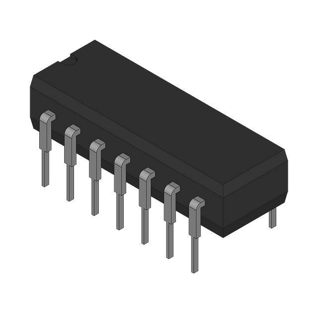
DIP & SOIC
© 2001 National Semiconductor Corporation
DS012751
www.national.com
CLC415 Quad, Wideband Monolithic Op Amp
December 2001
�CLC415
Ordering Information
Package
Temperature Range
Industrial
Part Number
Package Marking
NSC Drawing
14-pin plastic DIP
−40˚C to +85˚C
CLC415AJP
CLC415AJP
N14A
14-pin plastic SOIC
−40˚C to +85˚C
CLC415AJE
CLC415AJE
M14A
www.national.com
2
�Operating Temperature Range
Storage Temperature Range
Lead Temperature (Soldering 10 sec)
ESD Rating (Human Body Model)
If Military/Aerospace specified devices are required,
please contact the National Semiconductor Sales Office/
Distributors for availability and specifications.
Supply Voltage (VCC)
IOUT
Output is short circuit protected to
ground, but maximum reliability will
be maintained if IOUT does not
exceed...
Common Mode Input Voltage
Differential Input Voltage
Maximum Junction Temperature
± 7V
−40˚C to +85˚C
−65˚C to +150˚C
+300˚C
< 1000V
Operating Ratings
Thermal Resistance
Package
MDIP
SOIC
60mA
± VCC
± 10V
+150˚C
(θJC)
55˚C/W
45˚C/W
(θJA)
105˚C/W
115˚C/W
Electrical Characteristics
(AV = +6, VCC = ± 5V, RL = 100Ω, Rf = 500Ω; Unless Specified)
Symbol
Parameter
Ambient Temperature
Conditions
CLC415AJ
Typ
Max/Min
(Note 2)
Units
+25˚C
+25˚C
−40˚C
+85˚C
VOUT < 2VPP
160
120
> 120
> 85
> 120
> 90
> 90
> 80
MHz
VOUT < 5VPP
< 0.2
< 0.5
< 0.7
< 1.0
< 0.08
< 0.10
< 0.08
< 0.10
< 60
< 63
< 0.2
< 0.5
< 0.7
< 1.0
< 0.08
< 0.10
< 0.08
< 0.10
< 60
< 63
< 0.2
< 0.5
< 1.1
< 1.3
< 0.08
< 0.10
< 0.08
< 0.10
< 59
< 62
dB
< 3.0
< 4.0
< 18
< 12
> 1200
< 3.0
< 3.6
< 18
< 12
> 1200
< 4.0
< 4.5
< 22
< 12
> 1000
Frequency Domain Response
SSBW
-3dB Bandwidth
LSBW
Gain Flatness
VOUT < 2VPP
GFPL
Peaking
DC to 25MHz
0
GFPH
Peaking
> 25MHz
0
Rolloff
GFR
DC to 50MHz
0.2
LPD
Linear Phase Deviation
DC to 75MHz
0.5
DG1
Differential Gain (AV = +2)
150Ω Load, 3.58MHz
0.03
150Ω Load, 4.43MHz
0.03
150Ω Load, 3.58MHz
0.03
150Ω Load, 4.43MHz
0.03
DG2
DP1
Differential Phase (AV = +2)
DP2
MHz
XT
Crosstalk Input Referred
5MHz (All Hostile)
65
CXT
Crosstalk Input Referred
5MHz (Chan. to Chan.)
70
2V Step
2.0
dB
dB
deg
%
%
deg
deg
dB
dB
Time Domain Response
TRS
Rise and Fall Time
TRL
5V Step
3.0
TS
Settling Time to 0.1%
2V Step
12
OS
Overshoot
2V Step
8
SR
Slew Rate
1500
ns
ns
ns
%
V/µs
Distortion And Noise Response
HD2
2nd harmonic distortion
2VPP,20MHz
−44
HD3
3rd harmonic distortion
2VPP, 20MHz
−54
< −38
< −46
< −38
< −46
< −34
< −42
dBc
dBc
Equivalent Input Noise
VN
Non-Inverting Voltage
> 1MHz
3.0
< 3.6
< 3.6
< 4.0
nV/
ICN
Inverting Current
> 1MHz
11.5
< 14
< 14
< 16
pA/
NCN
Non-Inverting Current
> 1MHz
2.0
< 2.6
< 2.6
< 3.0
pA/
SNF
Total Noise Floor
37
< −155
< 44
< −155
< 44
< −154
< 48
dBm1Hz
Total Integrated Noise
> 1MHz
> 1MHz to 100MHz
−157
INV
2
45
< 27
> 47
> 45
< 26
> 45
> 43
< 24
> 600
< 2.0
< 0.3
> 600
< 2.0
< 0.2
kΩ
0.2
> 300
< 2.0
< 0.6
± 2.6
± 2.2
± 2.3
± 1.4
± 2.5
± 2.0
± 2.5
± 2.0
V
60
50
50
50
mA
DVIO
Average Temperature
Coefficient
IBN
Input Bias Current (Note 3)
DIBN
Average Temperature
Coefficient
IBI
Input Bias Current (Note 3)
DIBI
Average Temperature
Coefficient
20
PSRR
Power Supply Rejection Ratio
55
CMRR
Common Mode Rejection Ratio
ICC
Supply Current, All Channels
Non Inverting
30
Inverting
3
50
No Load
20
-
µA
µA
dB
dB
mA
Miscellaneous Performance
RIN
Non-Inverting Input Resistance
1300
CIN
Non-Inverting Input Capacitance
RO
Output Impedance
DC
VO
Output Voltage Range
RL = 100Ω
CMIR
Common Mode Input Range
IO
Output Current
1.0
pF
Ω
V
Note 1: “Absolute Maximum Ratings” are those values beyond which the safety of the device cannot be guaranteed. They are not meant to imply that the devices
should be operated at these limits. The table of “Electrical Characteristics” specifies conditions of device operation.
Note 2: Max/min ratings are based on product characterization and simulation. Individual parameters are tested as noted. Outgoing quality levels are determined
from tested parameters.
Note 3: AJ-level: spec. is 100% tested at +25˚C.
www.national.com
4
�(TA = 25˚, AV = +6, VCC = ± 5V, RL = 100Ω, Rf = 500Ω; Un-
less Specified).
Non-Inverting Frequency Response
Inverting Frequency Response
DS012751-1
Frequency Response for Various RLS
DS012751-2
Small Signal Pulse Response
DS012751-4
DS012751-3
Short-Term Settling Time
Long-Term Settling Time
DS012751-5
DS012751-6
5
www.national.com
CLC415
Typical Performance Characteristics
�CLC415
Typical Performance Characteristics
(TA = 25˚, AV = +6, VCC = ± 5V, RL = 100Ω, Rf = 500Ω;
Unless Specified). (Continued)
2nd and 3rd Harmonic Distortion
2-Tone, 3rd Order, Spurious Levels
DS012751-7
Settling Time vs. Capacitive Load
DS012751-8
All-Hostile Crosstalk Isolation
DS012751-10
DS012751-9
Most Susceptible Channel-Channel Pulse Coupling
Differential Gain and Phase (4.43 MHz, AV = +2)
DS012751-11
DS012751-12
www.national.com
6
�(TA = 25˚, AV = +6, VCC = ± 5V, RL = 100Ω, Rf = 500Ω;
Unless Specified). (Continued)
Equivalent Input Noise
Open-Loop Transimpedance Gain, Z(s)
DS012751-13
DS012751-14
PSRR, CMRR, and Closed Loop RO
DS012751-15
7
www.national.com
CLC415
Typical Performance Characteristics
�CLC415
Application Division
Feedback Resistor
Non-Inverting Source Impedance
The CLC415 achieves its exceptional AC performance while
requiring very low quiescent power by using the current
feedback topology and an internal slew rate enhancement
circuit. The loop gain and frequency response for a current
feedback op amp is predominantly set by the feedback
resistor value. The CLC415 is optimized for a gain of +6 to
use a 500Ω feedback resistor (use a 900Ω Rf for maximally
flat response at a gain of +2). Using lower values can lead
to excessive ringing in the pulse response while higher value
will limit the bandwidth.
Application Note OA-13 provides a more detailed discussion
of choosing a feedback resistor. The equations found in this
application note are to be considered a starting point for the
determination of Rf at any gain. The value of input impedance for the CLC415 is approximately 60Ω. These equations
do not account for parasitic capacitance at the inverting input
nor across Rf. The plot found below entitled “Recommended
Rf vs. Gain” offers values of Rf which will optimize the
frequency response of the CLC415 over its ± 1 to ± 10 gain
range. Unlike voltage feedback, current feedback op amps
require a non-zero Rf for unity gain followers.
For best operation, the DC source impedance looking out of
the non-inverting input should be less than 3kΩ but greater
than 20Ω. Parasitic self oscillations may occur in the input
transistors if the DC source impedance is out of this range.
This impedance also acts as the gain for the non-inverting
input bias and noise currents and therefore can become
troublesome for high values of DC source impedance. The
inverting configuration of Figure 3 shows a 25Ω resistor to
ground on the non-inverting input which insures stability but
does not provide bias current cancellation. The input bias
currents are unrelated for a current feedback amplifier which
eliminates the need for source impedance matching to
achieve bias current cancellation.
DS012751-17
FIGURE 3. Recommended Inverting Gain Circuit
DC Accuracy and Noise
Please refer to the application information section of the
CLC406 for a discussion of output offset voltage and spot
noise calculation.
Crosstalk
In any multi-channel integrated circuit there is an undesirable tendency for the signal in one channel to couple with
and reproduce itself in the output of another channel. This
effect is referred to as crosstalk. Crosstalk is expressed as
channel separation or channel isolation which indicates the
magnitude of this undesirable effect. This effect is measured
by driving one or more channels and observing the output of
the other undriven channel(s). The CLC415 plot page offers
two different graphs detailing the effect of crosstalk over
frequency. One plot entitled “All-Hostile Crosstalk Isolation”
graphs all-hostile, input referred crosstalk. All-hostile
crosstalk refers to the condition where three channels are
driven simultaneously while observing the output of the undriven fourth channel. Input-referred implies that crosstalk is
directly affected by gain and therefore a higher gain increases the crosstalk effect by a factor equal to that gain
setting.
The
plot
entitled
“Most
Susceptible
Channel-to-Channel Pulse Coupling” describes the effect of
crosstalk when one channel is driven with a 2VPP pulse while
the output of the most effected channel is observed.
DS012751-19
FIGURE 1. Recommended Rf vs. Gain
DS012751-16
FIGURE 2. Recommended Non-Inverting Gain Circuit
www.national.com
8
�ticular importance is the careful control of parasitic capacitances on the output pin. As the output impedance plot
shows, the closed loop output for the CLC415 eventually
becomes inductive as the loop gain rolls off with increasing
frequency. Direct capacitive loading on the output pin can
quickly lead to peaking in the frequency response, overshoot
in the pulse response, ringing or even sustained oscillations.
The “Settling Time vs. Capacitive Load” plot should be used
as a starting point for the selection of a series output resistor
when a capacitive load must be driven. A quad amplifier will
require careful attention to signal routing in order to minimize
the effects of crosstalk. Signal coupling through the power
supplies can be reduced with bypass capacitors placed
close to the device supply pins.
Evaluation Board
Evaluation PC boards (part number CLC730024 for
through-hole and 730031 for SOIC) for the CLC415 are
available.
(Continued)
Unused Amplifiers
It is recommended that any unused amplifiers in the quad
package be connected as unity gain followers (Rf =500Ω)
with the non-inverting input tied to ground through a 50Ω
resistor.
Slew Rate and Harmonic Distortion
Please see the application information for the CLC406.
Differential Gain and Phase
Differential gain and phase performance specifications are
common to composite video distribution applications. These
specifications refer to the change in small signal gain and
phase of the color subcarrier frequency (4.43MHz for PAL
composite video) as the amplifier output is swept over a
range of DC voltages. Application Note OA-08 provides an
additional discussion of differential gain and phase measurements.
Printed Circuit Layout
As with any high speed component, a careful attention to the
board layout is necessary for optimum performance. Of par-
9
www.national.com
CLC415
Application Division
�CLC415
Physical Dimensions
inches (millimeters) unless otherwise noted
14-Pin MDIP
NS Package Number N14A
14-Pin SOIC
NS Package Number M14A
www.national.com
10
�CLC415 Quad, Wideband Monolithic Op Amp
Notes
LIFE SUPPORT POLICY
NATIONAL’S PRODUCTS ARE NOT AUTHORIZED FOR USE AS CRITICAL COMPONENTS IN LIFE SUPPORT
DEVICES OR SYSTEMS WITHOUT THE EXPRESS WRITTEN APPROVAL OF THE PRESIDENT AND GENERAL
COUNSEL OF NATIONAL SEMICONDUCTOR CORPORATION. As used herein:
1. Life support devices or systems are devices or
systems which, (a) are intended for surgical implant
into the body, or (b) support or sustain life, and
whose failure to perform when properly used in
accordance with instructions for use provided in the
labeling, can be reasonably expected to result in a
significant injury to the user.
National Semiconductor
Corporation
Americas
Email: support@nsc.com
www.national.com
National Semiconductor
Europe
Fax: +49 (0) 180-530 85 86
Email: europe.support@nsc.com
Deutsch Tel: +49 (0) 69 9508 6208
English Tel: +44 (0) 870 24 0 2171
Français Tel: +33 (0) 1 41 91 8790
2. A critical component is any component of a life
support device or system whose failure to perform
can be reasonably expected to cause the failure of
the life support device or system, or to affect its
safety or effectiveness.
National Semiconductor
Asia Pacific Customer
Response Group
Tel: 65-2544466
Fax: 65-2504466
Email: ap.support@nsc.com
National Semiconductor
Japan Ltd.
Tel: 81-3-5639-7560
Fax: 81-3-5639-7507
National does not assume any responsibility for use of any circuitry described, no circuit patent licenses are implied and National reserves the right at any time without notice to change said circuitry and specifications.
�National P/N CLC415 - Quad, Wideband Monolithic Op Amp
See A/D Converters
Products
Products > Analog - Amplifiers > Operational Amplifiers > Legacy High Speed > CLC415
CLC415 Product Folder
Quad, Wideband Monolithic Op Amp
See Also: LMH6644 - LOWER COST
Generic P/N 415
General
Description
Features
Datasheet
Parametric Table
Package
& Models
Samples
& Pricing
Design
Tools
Application
Notes
Parametric Table
Channels (Channels)
4
Feedback Type
Current
Input Output Type
Not Rail to Rail
BW at Av+1 (MHz)
260
Bandwidth, typ (MHz)
259
BW at Av+2 (MHz)
240
Slew Rate, typ (Volts/usec)
1500
BW at Av+5 (MHz)
170
Supply Current per Channel, typ (mA)
5
BW at Av+10 (MHz)
101
Minimum Supply Voltage (Volt)
10
BW at Av+20 (MHz)
-
Maximum Supply Voltage (Volt)
14
HD 2nd, typ (dB)
-44
Offset Voltage, Max (mV)
5
HD 3rd, typ (dB)
-54
Input Bias Current, Temp Max (nA)
25000
DG, typ (dB)
.03
Output Current, typ (mA)
70
DP, typ (%)
.03
Voltage Noise, typ (nV/Hz)
3
Settling Time
12nS to 0.1%
Shut down
No
Special Features
-
Datasheet
Title
CLC415 Quad, Wideband Monolithic Op Amp
CLC415 Quad, Wideband Monolithic Op Amp
(JAPANESE)
CLC415 Mil-Aero Datasheet MNCLC415A-X
Size in
Date
Kbytes
View Online Download
7279
Dec- View Online
Kbytes
01
Download
386
Kbytes
View Online
Download
89
Kbytes
View Online
Download
Receive via
Email
Receive via
Email
Receive via
Email
Receive via
Email
If you have trouble printing or viewing PDF file(s), see Printing Problems.
file:///H|/imaging/BITTING/cpl/20020808_1/08062002_10/NATL/08062002_HTML/CLC415.html (1 of 4) [Aug-08-2002 5:37:37 PM]
�National P/N CLC415 - Quad, Wideband Monolithic Op Amp
Package Availability, Models, Samples & Pricing
Part
Number
Package
Status
Type
Budgetary
Samples &
Pricing
Electronic
$US
Orders
IBIS
Qty
each
Models
Pins MSL
SPICE
Std
Pack
Size
Package
Marking
CLC415AJE
SOIC
NARROW
14
MSL
Lifetime
buy
clc415.cir N/A
1K+ $5.0500
rail
of
55
[logo]¢U¢Z¢2¢T
CLC415AJE
CLC415AJETR13
SOIC
NARROW
14
MSL
Lifetime
buy
clc415.cir N/A
1K+ $5.0500
reel
of
2500
[logo]¢U¢Z¢2¢T
CLC415AJE
CLC415AJMPR
CERDIP
14
MSL Preliminary clc415.cir N/A
59629305501MCA
CERDIP
14
MSL
Full
clc415.cir N/A
production
rail [logo]¢Z¢S¢4¢A$E
of
CLC415AJ-MPR
N/A
PROTO
Buy Now
25+ $42.5000
rail
of
25
[logo]¢Z¢S¢4¢A$E
CLC415AJ-QML
5962-9305501MCA
General Description
The CLC415 is a wideband, quad, monolithic operational amplifier designed for intermediate gain applications
where power and cost per channel of are primary concern. Benefiting from National's current feedback
architecture, the CLC415 offers a gain range of ±1 to ±10 while providing stable, oscillation free operation
without external compensation, even at unity gain.
Operating from ±5V supplies, the CLC415 consumes only 50mW of power per channel, yet maintains a
160MHz small-signal bandwidth and a 1500V/µs slew rate. High density applications requiring an integrated
solution will enjoy the CLC415's 70dB channel isolation (input referred @ 5MHz).
With its exceptional differential gain and phase, typically 0.03% and 0.03° @ 3.58MHz, the CLC415 is
designed to meet the performance and cost per channel requirements of high volume composite video
applications. The CLC415's large-signal bandwidth, high slew rate and high drive capability are features well
suited for RGB-video applications.
The CLC415 is a quad version of the high speed CLC406 while the CLC414 is a lower power quad version of
the same. Both of these quads afford the designer lower power consumption and lower cost per channel with
the additional benefit of requiring less board space per amplifier.
Constructed using an advanced, complementary bipolar process and National's proven current feedback
architectures. The CLC415 is available in several versions to meet a variety of requirements.
Enhanced Solutions (Military/Aerospace)
SMD Number: 5962-93055
Space level versions also available.
For more information, visit http://www.national.com/mil
Features
file:///H|/imaging/BITTING/cpl/20020808_1/08062002_10/NATL/08062002_HTML/CLC415.html (2 of 4) [Aug-08-2002 5:37:37 PM]
�National P/N CLC415 - Quad, Wideband Monolithic Op Amp
●
●
●
●
●
●
●
●
160MHz small signal bandwidth
5mA quiescent current per amplifier
70dB channel isolation @ 5MHz
0.03%/0.03° differential gain/phase
12ns settling to 0.1%
1500V/µs slew rate
2.0ns rise and fall time (2VPP)
60mA output current per amplifier
Applications
●
●
●
●
●
●
●
Composite video distribution amps
HDTV amplifiers
RGB-video amplifiers
CCD signal processing
Active Filters
Instrumentation differential amps
Channelized EW
Design Tools
Title
Size in Kbytes Date
Amplifiers Selection Guide
software for Windows
7 Kbytes
12-Jun2002
View
CLC730024EB 14 pin DIP Op
Amp Evaluation Board
85 Kbytes
27-Oct1998
View Online
Download
Receive via Email
CLC730031EB 14 pin SOIC Op
Amp Evaluation Board
85 Kbytes
27-Oct1998
View Online
Download
Receive via Email
View Online Download Receive via Email
If you have trouble printing or viewing PDF file(s), see Printing Problems.
Application Notes
Title
Size in Kbytes Date
View Online Download Receive via Email
OA-07: OA-07 Current- Feedback
308 Kbytes
Op Amp Applications Circuit
Guide
28-Oct-96 View Online
Download
Receive via Email
OA-11: OA-11 A Tutorial on
Applying Op Amps to RF
Applications
2-Apr-99
View Online
Download
Receive via Email
OA-12: OA-12 Noise Analysis for
108 Kbytes
Comlinear's Op Amps
24-Feb-99 View Online
Download
Receive via Email
OA-13: OA-13 Current- Feedback
527 Kbytes
Loop Gain Analysis
28-Oct-96 View Online
Download
Receive via Email
OA-14: OA-14 Improving
Amplifier Noise Figure for High
3rd Intercept Amplifiers
15-Dec-00 View Online
Download
Receive via Email
769 Kbytes
92 Kbytes
file:///H|/imaging/BITTING/cpl/20020808_1/08062002_10/NATL/08062002_HTML/CLC415.html (3 of 4) [Aug-08-2002 5:37:37 PM]
�National P/N CLC415 - Quad, Wideband Monolithic Op Amp
OA-15: OA-15 Frequent Faux Pas
527 Kbytes
in Applying Wideband Current
Feedback Amplifiers
28-Jan-99 View Online
Download
Receive via Email
OA-18: OA-18 Simulation SPICE
Models for Comlinear's Op Amps
23-May-00 View Online
Download
Receive via Email
337 Kbytes
OA-20: OA-20 Current Feedback
139 Kbytes
Myths Debunked
10-Jul-97
View Online
Download
Receive via Email
OA-25: OA-25 Stability Analysis
of Current Feedback Amplifier
262 Kbytes
10-Oct-96 View Online
Download
Receive via Email
OA-30: OA-30 Current vs.
Voltage Feedback Amplifiers
56 Kbytes
5-Jun-98
View Online
Download
Receive via Email
If you have trouble printing or viewing PDF file(s), see Printing Problems.
[Information as of 5-Aug-2002]
Search
Design
Purchasing
Quality
Company
Home
About Languages . Website Guide . About "Cookies" . National is QS 9000 Certified . Privacy/Security Statement .
Contact Us . Site Terms & Conditions of Use . Copyright 2002 © National Semiconductor Corporation . My Preferences .
Feedback
file:///H|/imaging/BITTING/cpl/20020808_1/08062002_10/NATL/08062002_HTML/CLC415.html (4 of 4) [Aug-08-2002 5:37:37 PM]
�


 工商网监
湘ICP备2023018690号
工商网监
湘ICP备2023018690号
